EP0183046A2 - Verfahren zur Verringerung der Rückkopplung in einem Halbleiterlaser eines optischen Datenspeichersystems - Google Patents
Verfahren zur Verringerung der Rückkopplung in einem Halbleiterlaser eines optischen Datenspeichersystems Download PDFInfo
- Publication number
- EP0183046A2 EP0183046A2 EP85113372A EP85113372A EP0183046A2 EP 0183046 A2 EP0183046 A2 EP 0183046A2 EP 85113372 A EP85113372 A EP 85113372A EP 85113372 A EP85113372 A EP 85113372A EP 0183046 A2 EP0183046 A2 EP 0183046A2
- Authority
- EP
- European Patent Office
- Prior art keywords
- laser
- layer
- opaque material
- semiconductor laser
- light
- Prior art date
- Legal status (The legal status is an assumption and is not a legal conclusion. Google has not performed a legal analysis and makes no representation as to the accuracy of the status listed.)
- Withdrawn
Links
Images
Classifications
-
- G—PHYSICS
- G11—INFORMATION STORAGE
- G11B—INFORMATION STORAGE BASED ON RELATIVE MOVEMENT BETWEEN RECORD CARRIER AND TRANSDUCER
- G11B7/00—Recording or reproducing by optical means, e.g. recording using a thermal beam of optical radiation by modifying optical properties or the physical structure, reproducing using an optical beam at lower power by sensing optical properties; Record carriers therefor
- G11B7/12—Heads, e.g. forming of the optical beam spot or modulation of the optical beam
- G11B7/125—Optical beam sources therefor, e.g. laser control circuitry specially adapted for optical storage devices; Modulators, e.g. means for controlling the size or intensity of optical spots or optical traces
- G11B7/127—Lasers; Multiple laser arrays
-
- H—ELECTRICITY
- H01—ELECTRIC ELEMENTS
- H01S—DEVICES USING THE PROCESS OF LIGHT AMPLIFICATION BY STIMULATED EMISSION OF RADIATION [LASER] TO AMPLIFY OR GENERATE LIGHT; DEVICES USING STIMULATED EMISSION OF ELECTROMAGNETIC RADIATION IN WAVE RANGES OTHER THAN OPTICAL
- H01S5/00—Semiconductor lasers
- H01S5/02—Structural details or components not essential to laser action
- H01S5/028—Coatings ; Treatment of the laser facets, e.g. etching, passivation layers or reflecting layers
Definitions
- This invention relates to semiconductor lasers and more particularly to a process for reducing feedback in a semiconductor laser used in an optical data storage system.
- Optical data storage disks are widely used in video disk and digital audio disk (DAD) systems.
- a high energy focused laser beam records the data as "data pits or holes" along an information track of an optical data storage disk.
- a low energy focused laser beam scans the recorded track and light reflected from the disk is sensed by a detector.
- One of the requirements of such systems is a constant output power of the recording laser.
- Semiconductor lasers are susceptible to output power fluctuations caused by light reflected back from the surface of the disk to the output facet of the laser. This reflected light re-enters the laser and distorts the lasing action within the laser. Reflected light re-entering the laser results in noise generation and an inaccurate signal from the photosensitive diode commonly mounted on the rear face of the laser for the purpose of monitoring laser power output. Either result can seriously interfere with optical recording.
- a conventional technique for preventing the light reflected back from the disk from re-entering the laser is to use a quarter wave plate and polarizing beam splitter.
- the best economical quarter wave plate systems provide a feedback reduction of only 10 to 10 .
- lasers used in optical data storage systems are sensitive to feedback as small as 10-4 or even less, this technique is not of itself sufficient and must be enhanced by the use of more expensive quarter wave plates or other supplemental means.
- the principal object of the invention is to provide a laser for use in an optical data storage system in which the light reflected back from the optical disk to an area adjacent the light exit aperture of the laser is prevented from entering the laser by modification of the laser itself, resulting in further reduction of feedback as compared with conventional methods.
- Another object of the invention is to provide an optical data storage system in which the sensitivity of the laser to feedback near its light exit aperture is reduced without the use of an additional component. This allows the technique to be easily added to existing systems to provide additional feedback reduction.
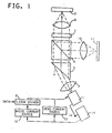
- a laser 1 for example, a semiconductor laser typically emitting a coherent beam of light at about 800 nm, which can be switched between a high and a low energy state, is driven by a laser driver 2.
- the data to be recorded is encoded using, for example, a conventional code of the type employed for magnetic recording, such as a run length limited (RLL) code.
- RLL run length limited
- the encoded data is applied to laser driver 2 to modulate a high energy laser beam emitted by laser 1 according to the encoded data pattern.
- the linearly polarized laser beam generated by laser 1 is collimated by a collimating lens 3.
- the collimated beam 4 is projected on a prism 5 at an appropriate angle to change its cross section from elliptical to circular.
- the circular collimated beam enters a polarizing beam splitter 6.
- the polarized beam passes through a quarter wave plate 7, which circularly polarizes the beam and passes it to an objective lens 8 which focuses it onto an optical disk 9 where it forms optically detectable changes such as pits or holes, in a selected track.
- laser 1 emits a low energy linearly polarized laser beam which passes through collimating lens 3, prism 5 and enters polarizing beam splitter 6.
- the polarized beam passes through quarter wave plate 7, which circularly polarizes the beam and passes it to objective lens 8 which focuses it onto optical disk 9.
- the beam reflected back from disk 9 is collected by objective lens 8 and passes through quarter wave plate 7 again.
- the beam is now converted back to a linearly polarized beam, but with a 90° rotation of the polarization with respect to the polarization of the incident beam, which causes it to be deflected by 90° when passing through polarizing beam splitter 6 and continues on through a lens 10 to a photodetector 11.
- Laser 1 is driven by a write current source 12 and by read current source 13 which provide a DC current at a level appropriate for read and write power requirements. Laser 1 is also connected to laser write driver 2 which provides the additional current pulses necessary to write the encoded optical data.
- the feedback control of read or write current function is accomplished with a monitor photodiode 14 usually located at the rear facet of the write laser.
- Photodiode 14 provides an output proportional to laser 1 output causing a corresponding reverse change in write and read current sources 12 and 13.
- Semiconductor lasers e.g. laser 1
- Quarter wave plate 7 and polarizing beam splitter 6 prevent most of the light reflected back from disk 9 from re-entering laser 1. Since commercial grade quarter wave plate systems provide a feedback reduction of 10 2 to 10 -3 and lasers used in optical data storage systems are sensitive to feedback as small as 10- 4 , this is not of itself sufficient to provide constant output power of the laser.
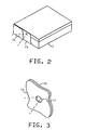
- FIG. 2 is a representation of laser 1 of FIG. 1, typically a GaAlAs semiconductor laser, modified according to the invention.
- a layer 15 of a protective and insulating material which is light transmissive, is applied onto the output facet of laser 1.
- Suitable protective and insulating materials include glasses commonly used with semiconductors, such as A1 2 0 3 , SiO 2 and SiO.
- Layer 15 protects the output facet of laser 1 from degradation by the subsequent processes and by the environmental conditions encountered. Layer 15 also keeps the following layer from electrically shorting the various layers of laser 1 together. By choosing the thickness of layer 15 equal to a quarter wavelength ( /4), the reflection of the front facet of laser 1 is reduced and also the efficiency of the light output from the lasing cavity is enhanced.
- a layer 16 of an opaque ablatable material is applied onto insulating layer 15.
- Suitable ablatable materials include Te, Au, Al, Ti and Te based alloys.
- the material is selected for maximum opacity and compatibility with the process of application and hole forming and with the other materials in the laser.
- the thickness is chosen to provide sufficient masking opacity and yet remain applicable and removable with an acceptable amount of time and energy.
- a typical thickness is about 1500 A.
- layers 15 and 16 can be made by means of a conventional vacuum deposition technique such as described in: "Thin Film Processes” edited by J. L. Vossen and W. Kern, Academic Press, 1978.
- the laser is first powered up to its normal maximum power.
- the opaque material of layer 16 is evaporated or melted away from the output beam cross-sectional area and forms an output window 17, as shown in FIG. 3. Since output window 17 has about the same area as the spot typically used at the optical disk surface for optical data recording, the energy density at window 17 will be sufficient to remove the opaque material.
- the process according to the invention provides a very simple solution to the problem of the light reflected back near the light exit aperture of the laser with a minimum of process step.
Landscapes
- Physics & Mathematics (AREA)
- Optics & Photonics (AREA)
- Optical Head (AREA)
- Semiconductor Lasers (AREA)
Applications Claiming Priority (2)
| Application Number | Priority Date | Filing Date | Title |
|---|---|---|---|
| US67711784A | 1984-11-30 | 1984-11-30 | |
| US677117 | 2000-09-29 |
Publications (2)
| Publication Number | Publication Date |
|---|---|
| EP0183046A2 true EP0183046A2 (de) | 1986-06-04 |
| EP0183046A3 EP0183046A3 (en) | 1988-01-07 |
Family
ID=24717406
Family Applications (1)
| Application Number | Title | Priority Date | Filing Date |
|---|---|---|---|
| EP85113372A Withdrawn EP0183046A3 (en) | 1984-11-30 | 1985-10-22 | Process for reducing feedback in a semiconductor laser used in an optical data storage system |
Country Status (2)
| Country | Link |
|---|---|
| EP (1) | EP0183046A3 (de) |
| JP (1) | JPS61134097A (de) |
Cited By (1)
| Publication number | Priority date | Publication date | Assignee | Title |
|---|---|---|---|---|
| EP0210582A3 (en) * | 1985-07-29 | 1988-12-21 | Mitsubishi Denki Kabushiki Kaisha | Optical head apparatus |
Families Citing this family (2)
| Publication number | Priority date | Publication date | Assignee | Title |
|---|---|---|---|---|
| JP2688897B2 (ja) * | 1987-03-13 | 1997-12-10 | シャープ株式会社 | 半導体レーザ装置 |
| JP2020129653A (ja) * | 2019-02-08 | 2020-08-27 | シャープ株式会社 | 発光素子及びその製造方法 |
Family Cites Families (2)
| Publication number | Priority date | Publication date | Assignee | Title |
|---|---|---|---|---|
| US4280107A (en) * | 1979-08-08 | 1981-07-21 | Xerox Corporation | Apertured and unapertured reflector structures for electroluminescent devices |
| FR2519813B1 (fr) * | 1982-01-08 | 1986-01-17 | Thomson Csf | Dispositif de stabilisation de la puissance optique d'un laser semi-conducteur |
-
1985
- 1985-07-16 JP JP60155293A patent/JPS61134097A/ja active Pending
- 1985-10-22 EP EP85113372A patent/EP0183046A3/en not_active Withdrawn
Cited By (1)
| Publication number | Priority date | Publication date | Assignee | Title |
|---|---|---|---|---|
| EP0210582A3 (en) * | 1985-07-29 | 1988-12-21 | Mitsubishi Denki Kabushiki Kaisha | Optical head apparatus |
Also Published As
| Publication number | Publication date |
|---|---|
| JPS61134097A (ja) | 1986-06-21 |
| EP0183046A3 (en) | 1988-01-07 |
Similar Documents
| Publication | Publication Date | Title |
|---|---|---|
| US4621353A (en) | Optical memory system providing improved focusing control and improved beam combining and separating apparatus | |
| CA1206612A (en) | Direct read after write optical disk system | |
| JP3201759B2 (ja) | 光磁気記録再生方法、この方法に用いるのに好敵な記録媒体並びに光磁気記録再生装置 | |
| EP0092113A2 (de) | Optisches Speicherelement zur Verwendung in einem optischen Speichersystem sowie ein Verfahren zur Herstellung des Speicherelements | |
| US6055223A (en) | Optical memory apparatus | |
| US5557601A (en) | Optical information recording/reproducing method and apparatus in which a first optical spot performs focusing, tracking, erasing and recording and a second optical spot performs two reproducing modes | |
| JP2602493B2 (ja) | 光学的データ記録装置 | |
| JPH02246030A (ja) | 光情報記録再生装置 | |
| JPH0581698A (ja) | 波長切換式光ピツクアツプ | |
| US4562568A (en) | Beam combining and separating apparatus useful for combining and separating reading and writing laser beams in an optical storage system | |
| JPS58158051A (ja) | 光学的記録再生装置 | |
| US4888759A (en) | Laser optical memory system having beam combining and separating apparatus for combining and separating reading and writing laser beams | |
| US5726961A (en) | Optical pickup control system for optical discs having different reflectivities | |
| JP3392206B2 (ja) | 光ピックアップ | |
| JPS62236152A (ja) | 光学式ピツクアツプ | |
| JPS61162838A (ja) | 光デイスク記録再生装置の光源駆動装置 | |
| JPS61134097A (ja) | 半導体レ−ザ−の製造方法 | |
| JPH0628700A (ja) | 記録再生用光学ヘッド | |
| JPH0922538A (ja) | エバネセント光ヘッド及び光情報記録再生装置 | |
| US4559622A (en) | Optical memory system providing improved focus detection and control by detecting reflected beam diameter variations at spaced predetermined locations in the system | |
| JPS62140253A (ja) | 光学的情報処理装置 | |
| JPH0213372B2 (de) | ||
| JP2738785B2 (ja) | 光磁気記録再生装置 | |
| JP2591637B2 (ja) | 光ヘッド | |
| KR100272368B1 (ko) | 고밀도 광기록재생매체 및 기록재생장치와 그 제조방법 |
Legal Events
| Date | Code | Title | Description |
|---|---|---|---|
| PUAI | Public reference made under article 153(3) epc to a published international application that has entered the european phase |
Free format text: ORIGINAL CODE: 0009012 |
|
| AK | Designated contracting states |
Kind code of ref document: A2 Designated state(s): DE FR GB |
|
| 17P | Request for examination filed |
Effective date: 19860919 |
|
| PUAL | Search report despatched |
Free format text: ORIGINAL CODE: 0009013 |
|
| AK | Designated contracting states |
Kind code of ref document: A3 Designated state(s): DE FR GB |
|
| 17Q | First examination report despatched |
Effective date: 19890621 |
|
| STAA | Information on the status of an ep patent application or granted ep patent |
Free format text: STATUS: THE APPLICATION IS DEEMED TO BE WITHDRAWN |
|
| 18D | Application deemed to be withdrawn |
Effective date: 19900103 |
|
| RIN1 | Information on inventor provided before grant (corrected) |
Inventor name: GONNELLA, NORMAN T. Inventor name: LUECKE, FRANCIS S. Inventor name: SODERSTROM, RONALD L. |