EP0183549A2 - Circuit de signalisation pour ligne d'abonné dans un système de télécommunications - Google Patents
Circuit de signalisation pour ligne d'abonné dans un système de télécommunications Download PDFInfo
- Publication number
- EP0183549A2 EP0183549A2 EP85308644A EP85308644A EP0183549A2 EP 0183549 A2 EP0183549 A2 EP 0183549A2 EP 85308644 A EP85308644 A EP 85308644A EP 85308644 A EP85308644 A EP 85308644A EP 0183549 A2 EP0183549 A2 EP 0183549A2
- Authority
- EP
- European Patent Office
- Prior art keywords
- subscriber line
- register means
- signalling device
- channel
- cyclically permutable
- Prior art date
- Legal status (The legal status is an assumption and is not a legal conclusion. Google has not performed a legal analysis and makes no representation as to the accuracy of the status listed.)
- Granted
Links
- 230000011664 signaling Effects 0.000 title claims abstract description 29
- 238000012360 testing method Methods 0.000 claims description 21
- 238000005070 sampling Methods 0.000 claims description 7
- 238000010586 diagram Methods 0.000 description 12
- 238000009432 framing Methods 0.000 description 12
- 238000001514 detection method Methods 0.000 description 3
- 230000001360 synchronised effect Effects 0.000 description 3
- 230000005540 biological transmission Effects 0.000 description 2
- 125000004122 cyclic group Chemical group 0.000 description 2
- 240000007320 Pinus strobus Species 0.000 description 1
- 230000001934 delay Effects 0.000 description 1
- 230000003111 delayed effect Effects 0.000 description 1
- 230000001419 dependent effect Effects 0.000 description 1
- 230000000694 effects Effects 0.000 description 1
- 238000013507 mapping Methods 0.000 description 1
- 238000000034 method Methods 0.000 description 1
- 230000000630 rising effect Effects 0.000 description 1
Images






Classifications
-
- H—ELECTRICITY
- H04—ELECTRIC COMMUNICATION TECHNIQUE
- H04Q—SELECTING
- H04Q11/00—Selecting arrangements for multiplex systems
- H04Q11/04—Selecting arrangements for multiplex systems for time-division multiplexing
-
- H—ELECTRICITY
- H04—ELECTRIC COMMUNICATION TECHNIQUE
- H04Q—SELECTING
- H04Q1/00—Details of selecting apparatus or arrangements
- H04Q1/18—Electrical details
- H04Q1/30—Signalling arrangements; Manipulation of signalling currents
- H04Q1/44—Signalling arrangements; Manipulation of signalling currents using alternate current
- H04Q1/444—Signalling arrangements; Manipulation of signalling currents using alternate current with voice-band signalling frequencies
- H04Q1/446—Signalling arrangements; Manipulation of signalling currents using alternate current with voice-band signalling frequencies using one signalling frequency
- H04Q1/448—Signalling arrangements; Manipulation of signalling currents using alternate current with voice-band signalling frequencies using one signalling frequency with conversion of a single frequency signal into a digital signal
Definitions
- This invention relates to a subscriber line signalling device for use in a telecommunications system.
- the invention has particular application to digital telecommunication exchange systems employing cyclically permutable codeword (c.p.c.) signalling.
- c.p.c. cyclically permutable codeword
- a subscriber line signalling device for use in a subscriber line interface module of a digital telecommunications system in which the device, being controlled by a microprocessor is arranged to generate and detect cyclically permutable code words on any of a plurality of independent traffic channel paths to or from the device respectively, each generated cyclically permutable code word on any one traffic channel path being synchronously coded with respect to any other channel path of the plurality of traffic channel paths by clock timing means.
- FIG. 1 shows a microprocessor A controlling a 32 byte two port processor interface B, a universal program bus selector C, a subscriber line signalling device or cyclically permutable code generator detector D, with which this invention is concerned, and, a subscriber line interface modem E.
- the microprocessor A communicates with the units B-E by way of the address/data bus ADDR/DATA.
- the microprocessor A receives signal INTO from unit E, generates signals RD, WR, for units B-E, signal ALE for units B, D, E and address latch AL and request signal BAR for unit B.
- Unit B acts as a two port buffer with arbitration between the shelf system bus and the microprocessor A.
- Unit B receives shelf control bus signals SCB and generates a transfer acknowledgement signal XACK and a signal RESET.
- a low order shelf address bus LO, and a high order shelf address bus HO is provided, the latter being connected to a module enable decoder MED, which receives a module position address bus MP.
- a data bus DB feeds into and out of the unit B.
- Unit B generates a decode signal CE for units C, D and E and a request granted signal BAG for the microprocessor A.
- the universal programmable bus selector C provides a common interface between six single channel digital traffic terminations operating at 32 K bits per second. It receives TDM signals at 1 M bit per second and transmits TDM signals out at 1 M bit per second.
- the unit has an address latch input to which the address latch AL is connected.
- the units A, B and C belong to a common area and the units D and E belong to a digital voice terminal interface area.
- the cyclic permutable code generator detector D detects and generates cyclically permutable codewords for any of six independent channels and is controlled by a standard microprocessor interface. Eleven registers provide command and status information for full control. A codeword is detected if incoming serial data contains any eight bit word repeated six times consecutively. Generation of a codeword is by continuous serial transmission of a data byte loaded by the control interface.
- the unit D receives traffic from units C and E and transmits traffic to units C and E.
- the subscriber line interface modem E interfaces between the multiplexed traffic highways from unit D and six line interface circuits LIC forming channel rate four wire digital voice terminal loops to the subscribers.
- Each of the units C, D and E receive a framing and a lMHz clock signal from a clock buffer CB.
- Each line interface circuit comprises trapezoidal line drivers LD, line receivers LR and a current limiter CL.
- the subscriber line inputs are shown as IP and the outputs OP.
- the subscriber line signalling device or cyclic permutable code generator detector D is arranged to detect and generate cyclically permutable codewords (c.p.c.) on any of six independent channels and is controlled by a standard microprocessor interface. Eleven registers provide command and status information for full device control. It is arranged that a c.p.c. is detected if incoming serial data contains any eight bit word repeated six times consecutively and that c.p.c. generation is a continuous serial transmission of data byte loaded by the control interface. Selectable comprehensive loopround modes allow the device, which is packaged in a 68 pin chip carrier, to be used in a variety of signalling and diagnostic applications.
- c.p.c. cyclically permutable codewords
- Fig. 1 illustrates a schematic diagram of the device D, ADDR/DATA representing the main address/data bus, other signals corresponding to those shown in Fig. 1 are as indicated, 32kb/sec traffic passes to and from the device and the universal programmable bus selector C by way of traffic ports PORT A IN and PORT B OUT and similarly to and from the subscriber line interface modem E by way of traffic ports PORT B IN and PORT B OUT.
- CLK represents the clock supplies which comprise the following:-
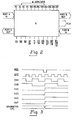
- Signals CKA, CKB, CKC, CKD, CKE and CKF are derived from the lMHz and framing input signals and are aligned as shown in Fig. 3. TABLE 1 should also be referred to. These signals may be used for multiplex/demultiplex functions on the traffic ports. The following inputs are provided to allow greater flexibility of operation.
- This c.p.c. generator detector interfaces six individual traffic channel paths in both send and return directions (Fig. 4). All traffic timing is synchronised by a single framing pulse FMG. Subsequent occurrences of the framing pulse may occur up to a frequency equal to the signalling rate.
- a c.p.c. detector is allocated to each channel.
- the detector recognises a serial data stream consisting of any eight-bit word repeated six times (48 bits total). If such a code is detected it is then reported as a c.p.c. to the microprocessor A. Repeat occurrences of that same word are ignored.
- a c.p.c. generator is also allocated to each channel.
- An eight-bit word is loaded by the control interface to a channel address. This word is then multiplexed into a continuous serial data stream. All channel multiplexers operate synchronously.
- the c.p.c. generator detector contains four read/write registers, seven read only registers and six write only registers. There are also three address locations reserved for functional testing purposes.
- Fig. 5 shows the address locations used within the device. Bit allocations within the bytes are shown in Fig. 6.
- Control information is loaded or read via eight bi-directional data lines under the control of the read, write and chip enable lines and an address latch is also used in multiplex mode.
- This read only register contains the code of the most recently received c.p.c.
- the c.p.c. detector operates continuously. If at any time a new c.p.c. is detected then this register will be re-loaded, whether or not the interrupt status flag is set. Re-loading will only be inhibited if the processor is engaged in a read cycle of this register. If a c.p.c. load is inhibited in this way the c.p.c. generator detector will make seven more attempts at lps intervals (16kb signalling), if all of these fail (due to the processor read) a completely new detection cycle will be initiated.
- This write only register is loaded with the c.p.c. code required to be generated.
- the generator operates continuously and cyclically transmits the byte loaded starting with bit 7.
- Bits 0 to 5 control the operational mode of channels A to F respectively.
- logic 1 sets traffic mode
- logic 0 sets signalling mode (see Fig. 7).
- Bits 0 to 5 control the diagnostic facility of channels A to F respectively. Setting a bit to 0 will enable the diagnostic facility of that channel (Fig. 7). This must be used in conjunction with the MODE command to select the required loopround.
- Bits 0 to 5 control channels A to F respectively.
- Logic 1 enables the channel into normal operation.
- Logic 0 will initiate a complete channel reset. All status and control bits associated with that channel will be cleared to logic 0; this affects interrupt status, receive and send c.p.c., mode and diagnostic registers.
- Bit 1 determines the signalling rate of all channels. A logic 0 forces 16 kbit/sec signalling. Logic 1 forces the device to 32 kbit/sec signalling.
- Bits 2 and 3 control the sampling point used by all the channel detectors. This facility enables the device to accept signalling information that is superimposed upon a faster data rate.
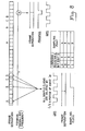
- the data rates that may be commanded are shown in Table 2 (See also Fig. 8).
- Bits 4, 5, 6 and 7 are read only bits and are set to logic 0.
- Test points for channels A to F are represented by bits 0 to 5. No test points are used during functional operation.
- Channels A to F are represented by bits 0 to 5.
- All traffic drivers are of open drain type.
- this input When set low this input enables the four bit address bus for internal register addressing. If set high it will disable the external address bus and select the latched data bus inputs for multiplexed addressing.
- ALE Address Latch Enable
- Address Latch Enable is used to latch into the address decoder an address set on the four least significant bits of the data bus. This input is normally set low if direct addressing has been selected. The address is latched on the low going edge of ALE.
- This input has the same effect as the software reset bit.
- active all registers are cleared to the 0 state including the software reset bit.
- This output will be active if any bit in the interrupt status register is set to logic 1.
- Output drive is open drain to allow wired or connection of multiple devices.
- Data input on the tri-state data bus is enabled into an addressed register when this pin and CHIP ENABLE are both held low. Data is latched on the rising edge of WRITE ENABLE.
- Data in an addressed register is enabled onto the tristate data bus if this pin and CHIP ENABLE are held low.
- This signal is not set all data lines are disabled. This reduces power consumption when other devices are using the control bus. This pin also disables the READ and WRITE inputs to allow memory mapping of the device.
- clock outputs are used to synchronously drive associated circuitry around the device (i.e. multiplexers and demultiplexers). Frequencies available are dependent upon the programmed signalling frequencies. (Table 1). Clocks will count down (+ve edge aligned). See Fig. 3.
- stage 2 FRAME counter will count at the same rate as the timeslot stage 1 counter. Used in conjunction with FRAMING all circuitry associated with the frame counter will be isolated to run at the new clock frequency.
- Timings given in this section represent the worst case delays over the permitted process spreads and an operating free air temperature of -55°C to +125°C. Power supply limits of 5v ⁇ 10% are assumed. Timings also include a load on all outputs of 50pF and are given in nano seconds.
- Timing numbers refer to Fig. 9 and Fig. 10. All timings are given in nano seconds.
- sampling point timing is shown in Fig. 8, detailed timing is as follows:
- Maximum frequency of the clock input (MEG) is 3.7 MHz.
- Fig. 11 shows a block diagram of all command and status registers common to every channel. All these registers are read directly by setting the appropriate address and holding CE and RE low.
- Stage 1 is synchronously cleared using the framing input (Fig. 8).
- This is a timeslot counter that synchronises all operations between consecutive bits of received c.p.c. data. It is used to determine the sampling point used by the detectors and to transmit two reference pulses that time the handling of interrupt calls.
- a borrow output feeds the second stage frame counter. This counts the number of frames (bits of c.p.c.) that pass and also provides a subtracted count.
- the first 3 bits of the second stage counter are delayed and demultiplexed into a one-of-eight code for the channel c.p.c. generators.
- the Stage 2 counter is cleared by the hardware or software reset inputs. If the test input is held low then the carry input to Stage 2 is forced active and the generators operate at the same speed as the Stage 1 counter.
- the test pin is not intended to facilitate testing of the receiver section, it is therefore recommended that any test program that uses the test input should also hold FMG low to prevent race hazards (this stops the Stage 1 counter).
- Fig. 13 Six detectors (Fig. 13) are provided, one for each channel. Basic operation is as follows. The sampling clock forces serial data to be shifted along a 9 bit shift register. A comparator compares bits 0 to 9 to determine if a c.p.c. is present, another comparator compares the shift register contents (first 8 bits) to the data in the 'c.p.c. received' status register. If these comparators indicate that the c.p.c. is invalid or old then a load pulse will be sent to the frame address store. Upon receipt of a load pulse the frame address store is loaded with the frame count -40.
- a third comparator compares the frame address store value with the true count, thus if the new c.p.c. has been valid for 40 frame counts a 'new c.p.c.' pulse will be generated by this comparator. This output is gated with Read enable to prevent read access violation.
- the detection sequence results in interrupt status (register and pin) outputs and the 'c.p.c. received' store being loaded with the shift register contents.
- the channel detection sequence is illustrated by the flow diagram shown in Fig. 15.
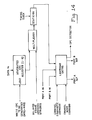
- Data to be transmitted is loaded into an 8 bit register (transparent latches). Frame address count strobes are used to multiplex this into a serial data stream, hence all channels transmit synchronously (Fig. 14). Loopround gating allows c.p.c. data to be transmitted or received from a variety of ports under control of the mode and diagnostic command register contents.
Landscapes
- Computer Networks & Wireless Communication (AREA)
- Engineering & Computer Science (AREA)
- Time-Division Multiplex Systems (AREA)
- Exchange Systems With Centralized Control (AREA)
- Interface Circuits In Exchanges (AREA)
- Devices For Supply Of Signal Current (AREA)
- Transmission Systems Not Characterized By The Medium Used For Transmission (AREA)
- Telephonic Communication Services (AREA)
- Monitoring And Testing Of Exchanges (AREA)
- Data Exchanges In Wide-Area Networks (AREA)
- Sheet Holders (AREA)
- Coupling Device And Connection With Printed Circuit (AREA)
- Steering Control In Accordance With Driving Conditions (AREA)
Priority Applications (1)
| Application Number | Priority Date | Filing Date | Title |
|---|---|---|---|
| AT85308644T ATE84391T1 (de) | 1984-11-28 | 1985-11-28 | Schaltung fuer teilnehmerleitungssignalisierung in einem vermittlungssystem. |
Applications Claiming Priority (2)
| Application Number | Priority Date | Filing Date | Title |
|---|---|---|---|
| GB848430005A GB8430005D0 (en) | 1984-11-28 | 1984-11-28 | Subscriber line signalling device |
| GB8430005 | 1984-11-28 |
Publications (3)
| Publication Number | Publication Date |
|---|---|
| EP0183549A2 true EP0183549A2 (fr) | 1986-06-04 |
| EP0183549A3 EP0183549A3 (en) | 1988-10-05 |
| EP0183549B1 EP0183549B1 (fr) | 1993-01-07 |
Family
ID=10570379
Family Applications (1)
| Application Number | Title | Priority Date | Filing Date |
|---|---|---|---|
| EP85308644A Expired - Lifetime EP0183549B1 (fr) | 1984-11-28 | 1985-11-28 | Circuit de signalisation pour ligne d'abonné dans un système de télécommunications |
Country Status (11)
| Country | Link |
|---|---|
| US (1) | US4737954A (fr) |
| EP (1) | EP0183549B1 (fr) |
| JP (1) | JPS61154295A (fr) |
| KR (1) | KR860004373A (fr) |
| AT (1) | ATE84391T1 (fr) |
| AU (1) | AU584370B2 (fr) |
| CA (1) | CA1238129A (fr) |
| DE (1) | DE3586963T2 (fr) |
| GB (2) | GB8430005D0 (fr) |
| GR (1) | GR852857B (fr) |
| NZ (1) | NZ214360A (fr) |
Cited By (1)
| Publication number | Priority date | Publication date | Assignee | Title |
|---|---|---|---|---|
| WO1998026508A1 (fr) * | 1996-12-12 | 1998-06-18 | Siemens Schweiz Ag | Procede et circuit pour le decodage d'un signal code cycliquement |
Families Citing this family (2)
| Publication number | Priority date | Publication date | Assignee | Title |
|---|---|---|---|---|
| US4991173A (en) * | 1988-10-17 | 1991-02-05 | Alcatel Na, Inc. | Apparatus and method for mapping of PCM signaling at signaling rate conversion boundaries |
| US7106820B2 (en) * | 2001-04-10 | 2006-09-12 | Broadcom Corporation | System and method for establishing word synchronization |
Family Cites Families (7)
| Publication number | Priority date | Publication date | Assignee | Title |
|---|---|---|---|---|
| US3863215A (en) * | 1973-07-03 | 1975-01-28 | Rca Corp | Detector for repetitive digital codes |
| JPS5518085B2 (fr) * | 1974-08-14 | 1980-05-16 | ||
| FR2442563A1 (fr) * | 1978-11-22 | 1980-06-20 | Materiel Telephonique | Dispositif de controle pour reseau de commutation temporelle |
| US4377843A (en) * | 1979-04-19 | 1983-03-22 | Wescom Switching, Inc. | Data distribution interface |
| DE2951914C2 (de) * | 1979-12-21 | 1982-04-01 | Siemens AG, 1000 Berlin und 8000 München | Verfahren zur Übertragung von Daten mit Hilfe eines Start-Stopsignals |
| GB2098834B (en) * | 1981-05-14 | 1985-02-13 | Standard Telephones Cables Ltd | Subscribers loop synchronisation |
| GB2120045B (en) * | 1982-04-22 | 1985-12-04 | Int Standard Electric Corp | Circuit for interfacing a processor to a line circuit |
-
1984
- 1984-11-28 GB GB848430005A patent/GB8430005D0/en active Pending
-
1985
- 1985-10-17 GB GB08525568A patent/GB2167624B/en not_active Expired
- 1985-11-27 GR GR852857A patent/GR852857B/el unknown
- 1985-11-27 US US06/802,140 patent/US4737954A/en not_active Expired - Fee Related
- 1985-11-27 JP JP60267040A patent/JPS61154295A/ja active Pending
- 1985-11-28 AT AT85308644T patent/ATE84391T1/de active
- 1985-11-28 DE DE8585308644T patent/DE3586963T2/de not_active Expired - Fee Related
- 1985-11-28 AU AU50464/85A patent/AU584370B2/en not_active Ceased
- 1985-11-28 KR KR1019850008899A patent/KR860004373A/ko not_active Ceased
- 1985-11-28 NZ NZ214360A patent/NZ214360A/xx unknown
- 1985-11-28 EP EP85308644A patent/EP0183549B1/fr not_active Expired - Lifetime
- 1985-11-28 CA CA000496443A patent/CA1238129A/fr not_active Expired
Cited By (1)
| Publication number | Priority date | Publication date | Assignee | Title |
|---|---|---|---|---|
| WO1998026508A1 (fr) * | 1996-12-12 | 1998-06-18 | Siemens Schweiz Ag | Procede et circuit pour le decodage d'un signal code cycliquement |
Also Published As
| Publication number | Publication date |
|---|---|
| GB2167624A (en) | 1986-05-29 |
| GB8525568D0 (en) | 1985-11-20 |
| ATE84391T1 (de) | 1993-01-15 |
| KR860004373A (ko) | 1986-06-20 |
| DE3586963T2 (de) | 1993-04-29 |
| US4737954A (en) | 1988-04-12 |
| GB2167624B (en) | 1988-08-03 |
| CA1238129A (fr) | 1988-06-14 |
| DE3586963D1 (de) | 1993-02-18 |
| EP0183549B1 (fr) | 1993-01-07 |
| AU584370B2 (en) | 1989-05-25 |
| AU5046485A (en) | 1986-06-05 |
| GB8430005D0 (en) | 1985-01-09 |
| EP0183549A3 (en) | 1988-10-05 |
| JPS61154295A (ja) | 1986-07-12 |
| GR852857B (fr) | 1986-03-28 |
| NZ214360A (en) | 1988-07-28 |
Similar Documents
| Publication | Publication Date | Title |
|---|---|---|
| US5805595A (en) | System and method for communicating packetized data over a channel bank | |
| EP0278949B1 (fr) | Multiplexeur-demultiplexeur a debit adaptatif | |
| US4603418A (en) | Multiple access data communications controller for a time-division multiplex bus | |
| EP0598052A1 (fr) | Procede et appareil d'attribution dynamique de largeur de bande dans une session de telecommunications numerique | |
| US5493565A (en) | Grooming device for streamlining a plurality of input signal lines into a grouped set of output signals | |
| US4392234A (en) | PCM Signal interface apparatus | |
| EP0190679A2 (fr) | Système de commutation de canaux temporels téléphoniques centralisé avec image sensible à l'état du réseau | |
| JPH05216688A (ja) | 共有リソースを割り付けるための決定論的方法 | |
| EP0175631B1 (fr) | Réseau numérique à intégration | |
| EP0183549A2 (fr) | Circuit de signalisation pour ligne d'abonné dans un système de télécommunications | |
| US5553066A (en) | Data transfer system including exchange | |
| EP0419750B1 (fr) | Mécanisme de distribution pour établir des communications entre des interfaces d'utilisateur d'un système de communication | |
| RU2105421C1 (ru) | Схема передачи-приема сигнальных данных системы коммутации цифровой сети комплексного обслуживания | |
| US6301623B1 (en) | Computer network with a plurality of identically addressed devices | |
| EP0183530B1 (fr) | Modem pour interface de ligne d'abonné | |
| US4815072A (en) | Switching arrangements for digital telecommunications exchange systems | |
| US3809819A (en) | Tdm switching apparatus | |
| JPH0759135A (ja) | 構内交換機及び該交換機に使用するラインカード | |
| KR100358386B1 (ko) | 전송장비에서의 서비스 대역폭 가변 할당장치 | |
| RU1797123C (ru) | Многоканальное устройство дл подключени абонентов к общей магистрали | |
| EP0351959A2 (fr) | Commande de canaux multiples | |
| US6396846B1 (en) | ISDN channel unit-resident mechanism for usurping time slots assigned to adjacent channel bank card slot | |
| EP0369116A2 (fr) | Commande de matrice de commutation MRT | |
| GB2157921A (en) | Multiplexer/demultiplexer | |
| JPH04373227A (ja) | 時分割多重化装置 |
Legal Events
| Date | Code | Title | Description |
|---|---|---|---|
| PUAI | Public reference made under article 153(3) epc to a published international application that has entered the european phase |
Free format text: ORIGINAL CODE: 0009012 |
|
| AK | Designated contracting states |
Kind code of ref document: A2 Designated state(s): AT BE CH DE FR IT LI LU NL SE |
|
| PUAL | Search report despatched |
Free format text: ORIGINAL CODE: 0009013 |
|
| AK | Designated contracting states |
Kind code of ref document: A3 Designated state(s): AT BE CH DE FR IT LI LU NL SE |
|
| 17P | Request for examination filed |
Effective date: 19890315 |
|
| RAP1 | Party data changed (applicant data changed or rights of an application transferred) |
Owner name: SIEMENS PLESSEY ELECTRONIC SYSTEMS LIMITED |
|
| 17Q | First examination report despatched |
Effective date: 19910404 |
|
| GRAA | (expected) grant |
Free format text: ORIGINAL CODE: 0009210 |
|
| AK | Designated contracting states |
Kind code of ref document: B1 Designated state(s): AT BE CH DE FR IT LI LU NL SE |
|
| REF | Corresponds to: |
Ref document number: 84391 Country of ref document: AT Date of ref document: 19930115 Kind code of ref document: T |
|
| ET | Fr: translation filed | ||
| ITF | It: translation for a ep patent filed | ||
| REF | Corresponds to: |
Ref document number: 3586963 Country of ref document: DE Date of ref document: 19930218 |
|
| PLBE | No opposition filed within time limit |
Free format text: ORIGINAL CODE: 0009261 |
|
| STAA | Information on the status of an ep patent application or granted ep patent |
Free format text: STATUS: NO OPPOSITION FILED WITHIN TIME LIMIT |
|
| PG25 | Lapsed in a contracting state [announced via postgrant information from national office to epo] |
Ref country code: AT Effective date: 19931128 |
|
| PG25 | Lapsed in a contracting state [announced via postgrant information from national office to epo] |
Ref country code: SE Effective date: 19931129 |
|
| PG25 | Lapsed in a contracting state [announced via postgrant information from national office to epo] |
Ref country code: LU Free format text: LAPSE BECAUSE OF NON-PAYMENT OF DUE FEES Effective date: 19931130 Ref country code: LI Effective date: 19931130 Ref country code: CH Effective date: 19931130 Ref country code: BE Effective date: 19931130 |
|
| 26N | No opposition filed | ||
| BERE | Be: lapsed |
Owner name: SIEMENS PLESSEY ELECTRONIC SYSTEMS LTD Effective date: 19931130 |
|
| PG25 | Lapsed in a contracting state [announced via postgrant information from national office to epo] |
Ref country code: NL Effective date: 19940601 |
|
| NLV4 | Nl: lapsed or anulled due to non-payment of the annual fee | ||
| PG25 | Lapsed in a contracting state [announced via postgrant information from national office to epo] |
Ref country code: FR Effective date: 19940729 |
|
| REG | Reference to a national code |
Ref country code: CH Ref legal event code: PL |
|
| PG25 | Lapsed in a contracting state [announced via postgrant information from national office to epo] |
Ref country code: DE Effective date: 19940802 |
|
| REG | Reference to a national code |
Ref country code: FR Ref legal event code: ST |
|
| EUG | Se: european patent has lapsed |
Ref document number: 85308644.5 Effective date: 19940610 |