EP0183722B1 - Halbleitermodulzusammenbau hoher dichte - Google Patents
Halbleitermodulzusammenbau hoher dichte Download PDFInfo
- Publication number
- EP0183722B1 EP0183722B1 EP85902283A EP85902283A EP0183722B1 EP 0183722 B1 EP0183722 B1 EP 0183722B1 EP 85902283 A EP85902283 A EP 85902283A EP 85902283 A EP85902283 A EP 85902283A EP 0183722 B1 EP0183722 B1 EP 0183722B1
- Authority
- EP
- European Patent Office
- Prior art keywords
- substrate
- die
- tapered
- holes
- chips
- Prior art date
- Legal status (The legal status is an assumption and is not a legal conclusion. Google has not performed a legal analysis and makes no representation as to the accuracy of the status listed.)
- Expired - Lifetime
Links
Images

Classifications
-
- H—ELECTRICITY
- H10—SEMICONDUCTOR DEVICES; ELECTRIC SOLID-STATE DEVICES NOT OTHERWISE PROVIDED FOR
- H10W—GENERIC PACKAGES, INTERCONNECTIONS, CONNECTORS OR OTHER CONSTRUCTIONAL DETAILS OF DEVICES COVERED BY CLASS H10
- H10W76/00—Containers; Fillings or auxiliary members therefor; Seals
- H10W76/10—Containers or parts thereof
- H10W76/12—Containers or parts thereof characterised by their shape
- H10W76/15—Containers comprising an insulating or insulated base
-
- H—ELECTRICITY
- H10—SEMICONDUCTOR DEVICES; ELECTRIC SOLID-STATE DEVICES NOT OTHERWISE PROVIDED FOR
- H10D—INORGANIC ELECTRIC SEMICONDUCTOR DEVICES
- H10D62/00—Semiconductor bodies, or regions thereof, of devices having potential barriers
- H10D62/10—Shapes, relative sizes or dispositions of the regions of the semiconductor bodies; Shapes of the semiconductor bodies
- H10D62/117—Shapes of semiconductor bodies
-
- H—ELECTRICITY
- H10—SEMICONDUCTOR DEVICES; ELECTRIC SOLID-STATE DEVICES NOT OTHERWISE PROVIDED FOR
- H10W—GENERIC PACKAGES, INTERCONNECTIONS, CONNECTORS OR OTHER CONSTRUCTIONAL DETAILS OF DEVICES COVERED BY CLASS H10
- H10W70/00—Package substrates; Interposers; Redistribution layers [RDL]
- H10W70/60—Insulating or insulated package substrates; Interposers; Redistribution layers
-
- H—ELECTRICITY
- H10—SEMICONDUCTOR DEVICES; ELECTRIC SOLID-STATE DEVICES NOT OTHERWISE PROVIDED FOR
- H10W—GENERIC PACKAGES, INTERCONNECTIONS, CONNECTORS OR OTHER CONSTRUCTIONAL DETAILS OF DEVICES COVERED BY CLASS H10
- H10W70/00—Package substrates; Interposers; Redistribution layers [RDL]
- H10W70/60—Insulating or insulated package substrates; Interposers; Redistribution layers
- H10W70/611—Insulating or insulated package substrates; Interposers; Redistribution layers for connecting multiple chips together
-
- H—ELECTRICITY
- H10—SEMICONDUCTOR DEVICES; ELECTRIC SOLID-STATE DEVICES NOT OTHERWISE PROVIDED FOR
- H10W—GENERIC PACKAGES, INTERCONNECTIONS, CONNECTORS OR OTHER CONSTRUCTIONAL DETAILS OF DEVICES COVERED BY CLASS H10
- H10W70/00—Package substrates; Interposers; Redistribution layers [RDL]
- H10W70/60—Insulating or insulated package substrates; Interposers; Redistribution layers
- H10W70/67—Insulating or insulated package substrates; Interposers; Redistribution layers characterised by their insulating layers or insulating parts
- H10W70/69—Insulating materials thereof
- H10W70/698—Semiconductor materials that are electrically insulating, e.g. undoped silicon
-
- H—ELECTRICITY
- H10—SEMICONDUCTOR DEVICES; ELECTRIC SOLID-STATE DEVICES NOT OTHERWISE PROVIDED FOR
- H10W—GENERIC PACKAGES, INTERCONNECTIONS, CONNECTORS OR OTHER CONSTRUCTIONAL DETAILS OF DEVICES COVERED BY CLASS H10
- H10W72/00—Interconnections or connectors in packages
- H10W72/50—Bond wires
- H10W72/531—Shapes of wire connectors
- H10W72/5363—Shapes of wire connectors the connected ends being wedge-shaped
-
- H—ELECTRICITY
- H10—SEMICONDUCTOR DEVICES; ELECTRIC SOLID-STATE DEVICES NOT OTHERWISE PROVIDED FOR
- H10W—GENERIC PACKAGES, INTERCONNECTIONS, CONNECTORS OR OTHER CONSTRUCTIONAL DETAILS OF DEVICES COVERED BY CLASS H10
- H10W72/00—Interconnections or connectors in packages
- H10W72/851—Dispositions of multiple connectors or interconnections
- H10W72/874—On different surfaces
- H10W72/884—Die-attach connectors and bond wires
-
- H—ELECTRICITY
- H10—SEMICONDUCTOR DEVICES; ELECTRIC SOLID-STATE DEVICES NOT OTHERWISE PROVIDED FOR
- H10W—GENERIC PACKAGES, INTERCONNECTIONS, CONNECTORS OR OTHER CONSTRUCTIONAL DETAILS OF DEVICES COVERED BY CLASS H10
- H10W74/00—Encapsulations, e.g. protective coatings
- H10W74/10—Encapsulations, e.g. protective coatings characterised by their shape or disposition
- H10W74/131—Encapsulations, e.g. protective coatings characterised by their shape or disposition the semiconductor body being only partially enclosed
- H10W74/142—Encapsulations, e.g. protective coatings characterised by their shape or disposition the semiconductor body being only partially enclosed the encapsulations exposing the passive side of the semiconductor body
-
- H—ELECTRICITY
- H10—SEMICONDUCTOR DEVICES; ELECTRIC SOLID-STATE DEVICES NOT OTHERWISE PROVIDED FOR
- H10W—GENERIC PACKAGES, INTERCONNECTIONS, CONNECTORS OR OTHER CONSTRUCTIONAL DETAILS OF DEVICES COVERED BY CLASS H10
- H10W90/00—Package configurations
-
- H—ELECTRICITY
- H10—SEMICONDUCTOR DEVICES; ELECTRIC SOLID-STATE DEVICES NOT OTHERWISE PROVIDED FOR
- H10W—GENERIC PACKAGES, INTERCONNECTIONS, CONNECTORS OR OTHER CONSTRUCTIONAL DETAILS OF DEVICES COVERED BY CLASS H10
- H10W90/00—Package configurations
- H10W90/10—Configurations of laterally-adjacent chips
Definitions
- This invention relates in general to electronic circuit modules, and, more particularly, to improved means and methods for providing high density circuit assemblies and modules having a multiplicity of interconnected integrated circuit chips or other components.
- Modern fabrication techniques make it possible to pack very large numbers of high speed semiconductor devices into individual integrated circuit (IC) chips or die.
- the individual ICs must be electrically interconnected in some way. Historically this has been done by mounting the individual IC die in sealed packages. These sealed packages protect the die from the environment and provide rugged external leads or pads which can be used for interconnecting the ICs in the system.
- the packaged die are generally mounted by their leads on a circuit board which contains the interconnect wiring.
- the circuit board often has multiple layers of interconnect wiring and may be fabricated of metallized plastics, ceramics, or impregnated paper or fabric.
- a significant disadvantage of this method is that the wiring length from die to die, through the individual packages and along the conductors of the circuit board, is many times the size of the IC die. With very high speed devices, these comparatively long wiring lengths cause significant propagation delays, reducing the overall system performance.
- Japanese Patent JP-A-59-44849 See Patent Abstract of Japan, vol 8, no. 135 (E-252) [1572], 22nd June 1984) shows a semi-conductor chip held by its side by a support plate of comparable thickness, the support plate having an aperture to receive the chip.
- Japanese Patent JP-A-53-46669 shows a plurality of semi-conductor chips mounted in tapered through holes in a ceramic support plate. Omitting the individual packages permits the die to be closer together, thus reducing the propagation delay in the circuit board.
- the IC die or chips have bonding pads which are connected to the wiring pattern on the circuit board by a variety of off-chip connection means; generally involving soldering or welding. Examples are wire bonds, flexible tapes, beam leads, and solder bumps.
- off-chip connection means generally involving soldering or welding. Examples are wire bonds, flexible tapes, beam leads, and solder bumps.
- a significant difficulty with these prior art approaches is that in most cases the metallurgy needed to make such off-chip connections is different than the metallurgy used for the on-chip interconnections within the IC chip. It is well known that the reliability of off-chip interconnections is substantially poorer than the reliability of on-chip interconnnections. Further, these prior art off-chip connections utilise much more area on the circuit board or substrate than is desired. This contributes to the comparatively low packing density of prior art circuit modules, even when the individual die packages are omitted, and the continued significant propagation delays associated therewith.
- Prior art modules have utilised materials having markedly different coefficients of thermal expansions. As a consequence thermal stresses are induced during temperature cycling. This further degrades reliability of the finished modules. Additionally, prior art modules have not provided simple and effective means for removal of heat. from the many IC chips or other components within the module. Thus, a need continues to exist for improved modules for integrated circuits and other components, particularly high density modules, having improved packing density, propagation delay, heat dissipation, ease of manufacture, and cost.
- semiconductor die prepared using different processing technologies (e.g. TTL, NMOS, linear, ECL, etc.) within the same monolithic substrate.
- an electrical structure comprising a plurality of semiconductor chips of a first thickness and a support means having a plurality of tapered through-holes for receiving the chips, and having joining means for holding the chips in the through-holes, is CHARACTERISED IN THAT the chips are integrated circuits having multiple contacts on one side thereof, each chip being oriented in a tapered hole with the contacts closest to the narrower end of said hole, the support means is of a thickness less than or equal to said first thickness of the semi-conductor chips, and the electrical structure further comprises leads formed by means of planar metallization technology mutually interconnecting the integrated circuits.
- a method for forming an electronic structure having a plurality of semiconductor dice of a first thickness and a contact location on a first surface thereof, wherein the dice are mounted in tapered through-holes in a support plate and retained therein by a filler material contacting an edge of the dice and a side of the support plate holes is CHARACTERISED BY said dice comprising integrated circuits having multiple contacts on the first surface thereof, and the steps of providing that said support plate is of a thickness less than or equal to said thickness of said dice, inserting the dice in the tapered through-hole with the contact location adjacent the narrower end of the tapered through-holes and forming leads by means of planar metallization technology to mutually interconnect the integrated circuits.
- the individual IC die are embedded in a support substrate so that their upper surfaces, on which the die connection points (e.g. contact pads) are located, are substantially co-planar with the surface of the substrate.
- the die are held by their edges. Any gaps between the substrate and the embedded die are filled so that the upper surface of the die, the upper surface of the gap filler material, and the upper surface of the substrate are substantially smooth and continuous.
- Conventional monolithic metallisation techniques can be used to form the inter-chip wiring within the module.
- This inter-chip wiring interconnects the various IC die embedded in the substrate and couples them to the external connection points of the module.
- the surfaces of the IC chips are covered with an insulating passivation layer, as is usually the case, the inter-chip wiring may pass over as well as between the individual ICs. Hence, packing density is maximised and propagation delay minimised.
- the substrate, the die, and the gap filling material have compatible thermal coefficients of expansion (TCEs), and it is desirable that they be similar. It is preferable that the same material be used for the substrate as is used for the semiconductor. Further, it is important that the surfaces on which the inter-chip wiring is placed be smooth, that is, free from sharp steps. Additionally, it is important that the rear faces of the die be co-planar and directly accessible to a heat sink plate, so that the escape of the heat generated within the die is not impeded by being required to pass through the substrate which supports the inter-chip wiring.
- TCEs thermal coefficients of expansion
- the substrate is also formed from silicon and the chips are mounted by their edges in through-holes in the substrate, preferably using a glass having a compatible coefficient of expansion.
- the substrate contains alignment means which are indexed to a heat sink in contact with the rear faces of the die.
- the heat sink is in turn indexed by other alignment means to an external connection support plate containing an array of connection pins. It is desirable that the heat sink and the connection support plate have substantially the same coefficient of expansion as the substrate, and preferably comprise the same material as used for the active devices, for example, silicon.
- the substrate with the embedded interconnected die, the heat sink, and the connection support plate are sealed together, preferably using a soldering material.
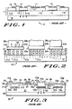
- FIG. 1 shows in schematic form, a cross-sectional view of a portion of a multi-chip integrated circuit electronic assembly or module according to the prior art
- FIG. 2 shows in schematic form, a cross-sectional view of a portion of a multi-chip integrated circuit electronic assembly or module according to another embodiment of the prior art
- FIG. 3 shows in schematic form, a cross-sectional view of a portion of a multi-chip integrated circuit electronic assembly or module according to a further embodiment of the prior art
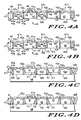
- FIGS. 4A-B show in schematic form, cross-sectional views of a portion of a multi-chip integrated circuit electronic assembly or module, and having IC chips of different thickness relative to the supporting substrate;
- FIGS. 4C-D show portions of modules similar to FIGS. 4A-B, in accordance with the present invention.
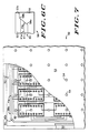
- FIG. 5 shows a top view of a portion of an electronic module according to the present invention
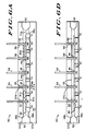
- FIG 6A shows in simplified form, a cross-sectional view of an electronic module, including a housing
- FIGS 6B-C show portions of the module of FIG. 6A according to further embodiments
- FIG. 6D shows in simplified form, a cross-sectional view of an electronic module
- FIG. 7 shows, in simplified form, a pin-side-up partial cut-away view of the module of FIG. 6A.
- FIG. 1 shows a schematic cross-section view of a portion of prior art IC assembly 10 comprising circuit board or substrate 11 having base portion 11a and wiring portion 11b.
- IC chips 12 are mounted face-up on base portion 11a by attachment means 13.
- IC chips 12 have bonding pads 14 which are connected by flexible wire or tape bonds 16 to corresponding pads 15 on interconnect wiring pattern 17 on surface 11c of wiring portion 11b of substrate 11. Heat is removed from IC chips 12 through attachment means 13 and substrate 11 to heat sink 18, as indicated by arrows 19.
- FIG. 2 shows a schematic cross-sectional view of a portion of prior art IC assembly 20 comprising circuit board or substrate 21 having buried wiring patterns indicated by dotted lines 21a-c which tie together bonding pads 25 on surface 21d of substrate 21.
- IC die 22a-c are mounted face-down onto substrate 21 by means of solder bumps 26 which connect bonding pads 24 on die 22a-c to pads 25 on substrate 21.
- Pads 24 and 25 are arranged so that they align. Heat is removed from rear surfaces 23a-c of die 22a-c directly to heat sinks 28a-c, as illustrated by arrows 29.
- FIG. 3 shows a schematic cross-sectional view of IC assembly 30, according to the prior art, in which die 32a-c are inset in cavities 33a-c in substrate 31. Die 32a-c are provided with beam leads 34 which bridge empty gaps 33g between die 32a-c and substrate 31. Beam leads 34 are welded or soldered to off-chip interconnect leads 36 or 37 on substrate 31. Leads 36 and 37 are separated by insulator 35 so that lead 36 can cross over lead 37 as needs be.
- Die 32a-c may be supported entirely by beam leads 34, as is indicated for die 32a in cavity 33a at the left of FIG. 3, or be attached to substrate 31 by solder means 33s at the bottom of the cavity, as indicated for die 32b-c in cavities 33b-c, at the right of FIG. 3.
- surfaces 32s of die 32a-c will be at a slightly different elevation than surface 31a of substrate 31.
- Beam leads 34 are deformable and can bend.
- differences in elevation of surfaces 31a and 32s can be accommodated, as is illustrated for die 32b and 32c. This permits die of different thickness to be placed in cavities of the same depth.
- FIG. 3 illustrates the situation where die 32a, die 32b, and die 32c all have different thicknesses.
- FIG. 3 suffers from several disadvantages. Chief among these are that beam leaded IC chips are very expensive to fabricate and assemble. Beam leads also require the use of metallurgy for the beams (e.g. Au) which is different than the metallurgy (e.g. Al) in most common use for on-chip wiring of integrated circuits. When different metallurgies are joined there is a greater likelihood of reliability problems. Hence when beam leads are used, the choice of interconnect materials available to the designer is more limited than when beam leads are not used. Further, beams leads 34 must be larger than normal metallization runs and so are wasteful of die and substrate area.
- metallurgy e.g. Au
- Al metallurgy
- heat can be conductively removed from die 32b-c only through solder means 33s and substrate 31, as illustrated by arrows 39 leading from die 32b through supporting substrate 31 to heat sink plate 38.
- Heat can be conductivity removed from die 32a only through beam leads 34, since die 32a makes no other contact with substrate 31. This results in a higher junction temperature for a given power dissipation level and reduces the reliability of the module.
- FIGS. 4A-B show cross-sectional views of a portion of monolithic IC assembly 40.
- Substrate 41 of monolithic assembly 40 contains through-holes 41h in which die 42 are held by their edges 42e by means of filler material 43f located in gaps 43g.
- Upper surfaces 42u of die 42, upper surface 41u of substrate 41, and upper surface 43u of gap filler material 43f are smoothly joined.
- Upper surface 42u of die 42 contains contact points 44 for making connection to the internal (on-chip) wiring of IC chip or die 42.
- Upper surface 41u of substrate 41 provides a smooth surface for supporting planar interconnect leads 46 and 47. Leads 46 and 47 differ in that lead 46 crosses over lead 47 by means of insulator 45. During fabrication, lead 47 is formed first. Cross-overs permit greater interconnection flexibility and are well known in the art.
- leads 46 and 47 can be formed by planar metallization techniques and extend from substrate surface 41u across gap filler surface 43u onto surface 42u of chip 42 to make contact directly to on-chip wiring contact points 44 of chips 42. This eliminates the need for wire bonds, beam leads, solder bumps, lead frames, and the like, as have been used in the prior art. There need be no welded or soldered connections between leads 46 and 47 on substrate 41, and connection points 44 on die 42, since intimate contact is made during the process by which leads 46 and 47 are fabricated.
- Planar metallization fabrication techniques are well known in the art and commonly used to provide interconnections within monolithic integrated circuits. As used herein, the words monolithic interconnections are intended to refer to interconnection made by planar metallization techniques. As used herein, the word monolithic refers to a continuous rigid body without voids or crevices.
- die 42 all have similar thickness 42t so that planar heat sink 48 may make intimate contact to die 42 without any need for articulation or for separate heat sinks for the individual die (see FIGS. 4C-D). As will be presently shown, this is readily obtained with the means and method of the present invention.
- Die 42 may be initially thinner than substrate 41. Substrate 41 is then lapped until substrate thickness 41t equals die thickness 42t. In the finished assembly, thickness 42t of die 42 must be at least equal to thickness 41t of substrate 41 so that die 42 may contact heat sink 48 without interference from substrate 41.
- FIGS. 4A and 4C illustrate the situation where some of die 42, e.g. die 42a-c, have thickness greater than the thickness of substrate 41
- FIGS. 4B and 4D illustrate the situation when die 42 have thickness equal to the thickness of substrate 41.
- lower faces 42L and 41L as well as upper faces 42u and 41u of die 42 and substrate 41, respectively, are substantially coplanar.
- FIGS. 4C-D there is direct contact between heatsink 48 and die 42, so that heat removal is particularly efficient.
- thickness 42t exceeds thickness 41t, a space can exist between substrate surface 41L and heat sink 48. This space may be empty, as shown in FIG. 4C, or filled, desirably with a heat conductive material.
- Gap filler material 43f mechanically joins die 42 to substrate 41.
- Gap 43g can be quite narrow, as for example, 1 mil (0.025 mm) or less. This permits gap filler material 43f to be quite thin (see FIGS. 4A-B).
- a suitable material for use as gap filler material 43f when die 42 are of silicon is type CF-6 glass manufactured by Nippon Electric Glass Co., Osaka, Japan, to which is added 10 to 20 volume percent of 2 to 10 micron particle size silicon dioxide. This glass mixture has a coefficient of thermal expansion, for 15% volume percent SiO2, of 39x10 ⁇ 7 per °C, in the range 25 to 300°C. Other glasses having coefficients of thermal expansion in the range of 30 to 45x10 ⁇ 7 per °C, and otherwise compatible with die 42 are also suitable. Plastic materials can also be used provided that they have adequate thermal stability to withstand subsequent processing steps and do not introduce significant mechanical stress.
- gap filler material 43f not shrink or crack during curing or firing so as to produce crevices in upper surface 43u or at the interfaces where gap filler material 43f joins die 42 and substrate 41. If die 42 are other than silicon, then filler material 43f should be chosen to have a coefficient of thermal expansion which is also compatible with the material comprising die 42. Generally, the relative thermal coefficients of expansion of substrate 41, die 42, and filler material 43f should be arranged so that filler 43f is in compression.
- FIGS 4A-B illustrate the situation where through-holes 41h have vertical side walls, i.e. substantially perpendicular to surface 41u.
- FIGS. 4C-D illustrate the situation where through-holes 41h have tapered side walls in accordance with the present invention.
- Such tapered holes are readily obtained using selective etching along preferred crystallographic planes. The use of tapered holes facilitates placement of die 42 in the through-holes.
- Contact points 44 on die 42 are interconnected by means of metallization runs or leads 46 and 47. Where cross-overs must occur, as for example between leads 46 and 47, insulating layer 45 is provided.
- Surfaces 42u, 41u, and 43u should be smooth, that is, there should not be abrupt steps in surface topology. As used herein, an abrupt step is defined as a change in surface topography or height greater than about 10% of the thickness of the layer intended to cover the step which occurs over a lateral distance less than the layer thickness.
- surfaces 41u, 42u, and 43u be substantially co-planar.
- surfaces 41u, 42u, and 43u are substantially co-planar, the surface topology does not contain large height differences which must be accommodated over short distances, and so abrupt surface steps are less likely.
- Surface smoothness is more important than absolute flatness or coplanarity. If surfaces 41u, 42u, and 43u join smoothly, i.e. without abrupt steps, then height differences of many times the thicknesses of the interconnect layers are easily accommodated.
- FIG. 5 shows a top view of an example of an assembly or module according to a preferred embodiment of the present invention.
- Monolithic assembly 40 contains a multiplicity of die 42 mounted in substrate 41 and having interconnections 46 and 47 tying on-chip contact points 44 of die 42 to each other and to external connection points 44a.
- insulating layer 45 between crossing metallization runs has been omitted and interconnect leads 46 and 47 are shown in schematic form.
- External connection points 44a are provided for connection of monolithic assembly 40 to the external system.
- External connection points 44a can overlie any portion of monolithic assembly 40, that is, they may be located on die 42, substrate 41, or gaps 43g.
- FIG. 5 illustrates the situation when monolithic assembly 40 contains ten die 42, each of which has eighteen contact points 44, for a total of one hundred and eighty die contact points. These one hundred and eighty die contact points 44 are interconnected by monolithic leads 46 and 47 which run across substrate 41, die 42, and filled gaps 43g. Interconnect leads 46 and 47, in this example, also couple die 42 to twenty five external connection points 44a.
- FIGS. 6A-C show cross sections of IC enclosure or module 50.
- Module 50 includes monolithic IC assembly 40. For clarity, most of the details of assembly 40, such as have been discussed in connection with FIGS. 4A-B and 5, have been omitted. External connection points 44a are shown.
- FIGS. 6B-C show portions of alternative arrangements, in less detail, of the periphery of module 50 of FIG. 6A.
- FIG. 6D shows an alternative arrangement in which assembly 40 forms an external wall of module 50 so as to provide for improved heat transfer to the external cooling means.
- Heat sink 51 of FIGS. 6A-C and 7 is analogous to heat sink 48 of FIGS. 4C-D.
- heat sink 51, seal ring 52, and connection substrate 53 also be of silicon.
- Pins 54 are insulated from connection substrate 53 by means of insulating layer 55, for example of silicon oxide.
- Connection means 56 for example solder bumps, allow output connection points 44a on IC assembly 40 to be coupled to output pins 54.
- Connection means 56 are in contact with connection points 44a which are coupled to leads 46 and 47.
- the direct thermal path from die 42 to heat sink 51 provides improved thermal coupling to the external cooling means as compared to the prior art arrangements, as indicated by arrows 69.
- Assembly 40, heat sink 51, and connection substrate 53 contain alignment keys so that when they are assembled, external connection pins 54 in connection substrate 53 line up with connection points 44a on assembly 40. This is facilitated by use of intermediate seal ring 52 which joins heat sink 51 at interface 57b and connection substrate 53 at interface 57a. Intermediate seal ring 52 is desirable but not essential, since, for example, connection substrate 53 can be shaped so as to mate directly with heat sink 51 on alignment surface 58c and interface 57b (see FIG. 6B). Alternatively, heat sink 51 can be shaped to mate directly with connection substrate 53 at interface 57a and alignment surface 58b (see FIG. 6C). Further, while heat sink 51 is desirable for increased strength, it is not essential and may be omitted, in which case substrate 41 of assembly 40 is extended to join directly to seal ring 52 and/or connection substrate 53. This is illustrated in FIG. 6D.
- FIG. 7 shows a pin-side-up partial cut-away view of module 50.
- Assembly 40 has perimeter 41p which matches surface 58a of heat sink 51, so that assembly 40 is laterally positioned in a predetermined location with respect to surface 58c (see FIG. 6A) which contacts seal ring 52.
- Alignment key 40k (see FIG. 7) provides azimuthal orientation of assembly 40 in heat sink 51.
- Perimeter 41p and alignment surfaces 58a-c are conveniently formed using known photolithographic masking techniques in conjunction with anisotropic etching. It is preferred to use anisotropic etching which takes advantage of the property of crystalline materials such as silicon to etch along determinable crystallographic planes.
- Connection pins 54 are located in known positions in connection substrate 53 by forming holes 59 for pins 54 and reference surface 58b in connection substrate 53 using photolithographic masking and etching techniques. Photolithograpic masking and etching techniques are capable of great precision so that precise alignment of the elements of module 50 may be conveniently obtained. Key 40k may be formed by any convenient means.
- Heat sink 51, and connection substrate 53 are conveniently joined to seal ring 52 by means of glass or metal seal means at interfaces 57a-b.
- Glass and or metal seal means can also be conveniently used at interface 57c between assembly 40 and heat sink 51, and at interface 57d between pins 54 and connection substrate 53.
- Techniques for joining semiconductors to each other and to other materials by use of glass and/or metal sealing or soldering are well known in the art. It is desirable that the sealing means used at interfaces 57a-d be compatible, that is, not introduce significant mechanical stress into the assembly. This is accomplished by choosing sealing and/or soldering materials which have coefficients of thermal expansion which are as close as practicable to the material used for enclosure 50.
- connection substrate 53 or assembly 40 Additional interconnection patterns may be placed on connection substrate 53 or assembly 40, and additional components may be mounted thereon if desired.
- chip capacitors 81a-b can be mounted on connection substrate 53 and/or substrate 40 (see FIG. 6A).
- die 42 are silicon ICs and that substrate 41 is of silicon.
- substrate 41 is of silicon.
- Substrate 41 is fabricated from a silicon starting wafer and then combined with die 42 to obtain monolithic assembly 40.
- the terms “upper surface” or “top surface” are intended to refer to surfaces 41u, 42u, and 43u of substrate 41, die 42, and gap filler material 43f, respectively, and on which are located contact points 44 and 44a, and interconnects 46 and 47.
- the terms “lower surface” or “bottom surface” are intended to refer to the major surface opposite the upper or top surface, for example, surface 42L of die 42 and surface 41L of substrate 41.
- Assembly 40 is fabricated as follows.
Landscapes
- Wire Bonding (AREA)
- Internal Circuitry In Semiconductor Integrated Circuit Devices (AREA)
Claims (8)
- Elektrisches Bauelement mit mehreren Halbleiterchips (42) in einer ersten Dicke und mit einem Träger (41), der mehrere sich verjüngende Durchgangslöcher zur Aufnahme der Chips (42) und der Zusammenfügung dienende Hilfsmittel (43) zum Festhalten der Chips (42) in den Durchgangslöchern aufweist,
DADURCH GEKENNZEICHNET, daß die Chips an ihrer einen Seite mehrere Kontakte aufweisende, integrierte Schaltungen sind, bei denen jedes Chip in dem sich verjüngenden Durchgangsloch derart orientiert ist, daß die Kontakte dem engeren Ende des Locnes am dichtesten liegen, daß der Träger eine Dicke besitzt, die geringer als die erste Dicke der Halbleiterchips oder gleich dieser ist, und daß das elektrische ßauelement ferner Leitungen (46, 47) enthält, die mit Hilfe einer planaren Metallisierungstechnik ausgebildet sind, durch die die integrierten Schaltungen gegenseitig verbunden werden. - Bauelement des Anspruches 1, bei dem die sich verjüngenden Durchgangslöcher in dem Träger einen etwas gerundeten Rand besitzen, an dem die sich verjüngenden Durchgangslöcher in eine Fläche des Trägers übergehen.
- Bauelement des Anspruches 2, bei dem der Träger ein einzelner Kristall ist und die Seite des sich verjüngenden Durchgangsloches im wesentlichen aus anisotrop geätzten, vorherbestimmten kristallographischen Ebenen besteht.
- Bauelement des Anspruches 3, bei dem der etwas abgerundete Rand durch isotropes Ätzen ausgebildet ist.
- Verfahren zur Ausbildung eines elektronischen Bauelementes mit mehreren würfelartigen Halbleiterstücken (42) in einer ersten Dicke, auf deren einer Fläche ein Kontakt angeordnet ist, wobei die würfelartigen Halbleiterstücke in sich verjüngenden Durchgangslöchern einer Trägerplatte (41) angebracht und in diesen von einem Füllmaterial (43) festgehalten werden, das mit einem Rand des Halbleiterstückes und einer Seite der Löcher in der Trägerplatte in Berührung steht, DADURCH GEKENNZEICHNET, daß jedes würfelartige Halbleiterstück, das integrierte Schaltungen enthält, auf seiner ersten Außenfläche mehrere Kontakte aufweist, daß die Trägerplatte, die eine Dicke besitzt, die geringer als die Dicke des würfelartigen Halbleiterstückes oder gleich dieser ist, daß das würfelartige Halbleiterstück in dem sich verjüngenden Durchgangsloch derart eingesetzt wird, daß sich die Kontakte neben dem engeren Ende der sich verjüngenden Durchgangslöcher befinden, und daß Leitungen (46, 47) mit Hilfe einer planaren Metallisierungstechnik ausgebildet werden, um die integrierten Schaltungen gegenseitig miteinander zu verbinden.
- Verfahren des Anspruches 5, bei dem ferner die Ränder des sich verjüngenden Durchgangsloches abgerundet werden.
- Verfahren des Anspruches 6, bei dem das Abrunden der Ränder in der Weise erfolgt, daß die Seite und die Ränder des sich verjüngenden Durchgangsloches isotrop geätzt werden.
- Verfahren nach Anspruch 5, dadurch gekennzeichnet, daß die Trägerplatte ein Einkristall ist und daß der Schritt des Ausbildens eines sich verjüngenden Durchgangsloches in der Trägerplatte das Formen des sich verjügenden Durchgangsloches vorzugsweise durch Ätzen umfaßt.
Applications Claiming Priority (2)
| Application Number | Priority Date | Filing Date | Title |
|---|---|---|---|
| US615499 | 1984-05-30 | ||
| US06/615,499 US4630096A (en) | 1984-05-30 | 1984-05-30 | High density IC module assembly |
Publications (3)
| Publication Number | Publication Date |
|---|---|
| EP0183722A1 EP0183722A1 (de) | 1986-06-11 |
| EP0183722A4 EP0183722A4 (de) | 1987-03-12 |
| EP0183722B1 true EP0183722B1 (de) | 1991-04-10 |
Family
ID=24465648
Family Applications (1)
| Application Number | Title | Priority Date | Filing Date |
|---|---|---|---|
| EP85902283A Expired - Lifetime EP0183722B1 (de) | 1984-05-30 | 1985-04-15 | Halbleitermodulzusammenbau hoher dichte |
Country Status (6)
| Country | Link |
|---|---|
| US (1) | US4630096A (de) |
| EP (1) | EP0183722B1 (de) |
| JP (1) | JPS61502294A (de) |
| DE (1) | DE3582480D1 (de) |
| IT (1) | IT1182219B (de) |
| WO (1) | WO1985005733A1 (de) |
Families Citing this family (78)
| Publication number | Priority date | Publication date | Assignee | Title |
|---|---|---|---|---|
| US4801561A (en) * | 1984-07-05 | 1989-01-31 | National Semiconductor Corporation | Method for making a pre-testable semiconductor die package |
| EP0244767A3 (de) * | 1986-05-05 | 1988-08-03 | Silicon Power Corporation | Hermetisches Halbleitergehäuse und Verfahren zum Herstellen |
| US4905075A (en) * | 1986-05-05 | 1990-02-27 | General Electric Company | Hermetic semiconductor enclosure |
| US4745455A (en) * | 1986-05-16 | 1988-05-17 | General Electric Company | Silicon packages for power semiconductor devices |
| US4792533A (en) * | 1987-03-13 | 1988-12-20 | Motorola Inc. | Coplanar die to substrate bond method |
| US4890156A (en) * | 1987-03-13 | 1989-12-26 | Motorola Inc. | Multichip IC module having coplanar dice and substrate |
| US4781775A (en) * | 1987-06-01 | 1988-11-01 | Motorola Inc. | Coplanar die to substrate bond method |
| FR2618255A1 (fr) * | 1987-07-14 | 1989-01-20 | Gen Electric | Bloc de conditionnement pour le montage et l'interconnexion de puces semiconductrices. |
| US4743568A (en) * | 1987-07-24 | 1988-05-10 | Motorola Inc. | Multilevel interconnect transfer process |
| FR2619665B1 (fr) * | 1987-08-21 | 1989-11-17 | France Etat | Dispositif de commande de l'eclairage de locaux |
| WO1989004113A1 (en) * | 1987-10-20 | 1989-05-05 | Irvine Sensors Corporation | High-density electronic modules, process and product |
| US5631447A (en) * | 1988-02-05 | 1997-05-20 | Raychem Limited | Uses of uniaxially electrically conductive articles |
| JPH0756887B2 (ja) * | 1988-04-04 | 1995-06-14 | 株式会社日立製作所 | 半導体パッケージ及びそれを用いたコンピュータ |
| JPH079953B2 (ja) * | 1988-04-13 | 1995-02-01 | 株式会社東芝 | 半導体装置の製造方法 |
| US5014114A (en) * | 1988-09-30 | 1991-05-07 | Harris Corporation | High speed, high density semiconductor memory package with chip level repairability |
| US5122475A (en) * | 1988-09-30 | 1992-06-16 | Harris Corporation | Method of making a high speed, high density semiconductor memory package with chip level repairability |
| US5055637A (en) * | 1989-05-02 | 1991-10-08 | Hagner George R | Circuit boards with recessed traces |
| US4985601A (en) * | 1989-05-02 | 1991-01-15 | Hagner George R | Circuit boards with recessed traces |
| US5098864A (en) * | 1989-11-29 | 1992-03-24 | Olin Corporation | Process for manufacturing a metal pin grid array package |
| US5103292A (en) * | 1989-11-29 | 1992-04-07 | Olin Corporation | Metal pin grid array package |
| US5006922A (en) * | 1990-02-14 | 1991-04-09 | Motorola, Inc. | Packaged semiconductor device having a low cost ceramic PGA package |
| US5081563A (en) * | 1990-04-27 | 1992-01-14 | International Business Machines Corporation | Multi-layer package incorporating a recessed cavity for a semiconductor chip |
| GB9014491D0 (en) * | 1990-06-29 | 1990-08-22 | Digital Equipment Int | Mounting silicon chips |
| US5241456A (en) * | 1990-07-02 | 1993-08-31 | General Electric Company | Compact high density interconnect structure |
| JP2623952B2 (ja) * | 1990-10-17 | 1997-06-25 | 日本電気株式会社 | 集積回路パッケージ |
| US5250843A (en) * | 1991-03-27 | 1993-10-05 | Integrated System Assemblies Corp. | Multichip integrated circuit modules |
| JPH06502744A (ja) * | 1991-03-27 | 1994-03-24 | インテグレイテッド システム アセンブリース コーポレーション | マルチチップ集積回路パッケージ及びモジュール |
| EP0547807A3 (en) * | 1991-12-16 | 1993-09-22 | General Electric Company | Packaged electronic system |
| US5432999A (en) * | 1992-08-20 | 1995-07-18 | Capps; David F. | Integrated circuit lamination process |
| US5323293A (en) * | 1992-12-18 | 1994-06-21 | International Business Machines Corporation | Arrangement for placing central processors and memory in a cryo cooled chamber |
| JP3156896B2 (ja) * | 1994-01-28 | 2001-04-16 | 富士通株式会社 | 半導体装置の製造方法およびかかる製造方法により製造された半導体装置 |
| US5541449A (en) * | 1994-03-11 | 1996-07-30 | The Panda Project | Semiconductor chip carrier affording a high-density external interface |
| US5521434A (en) * | 1994-10-17 | 1996-05-28 | International Business Machines Corporation | Semiconductor chip and electronic module with integrated surface interconnects/components |
| US5642262A (en) * | 1995-02-23 | 1997-06-24 | Altera Corporation | High-density programmable logic device in a multi-chip module package with improved interconnect scheme |
| US5841193A (en) * | 1996-05-20 | 1998-11-24 | Epic Technologies, Inc. | Single chip modules, repairable multichip modules, and methods of fabrication thereof |
| US7157314B2 (en) | 1998-11-16 | 2007-01-02 | Sandisk Corporation | Vertically stacked field programmable nonvolatile memory and method of fabrication |
| US6392159B1 (en) | 1999-07-27 | 2002-05-21 | International Business Machines Corporation | Embedded structure for engineering change and repair of circuit boards |
| US6255899B1 (en) | 1999-09-01 | 2001-07-03 | International Business Machines Corporation | Method and apparatus for increasing interchip communications rates |
| US6452265B1 (en) | 2000-01-28 | 2002-09-17 | International Business Machines Corporation | Multi-chip module utilizing a nonconductive material surrounding the chips that has a similar coefficient of thermal expansion |
| US8575719B2 (en) | 2000-04-28 | 2013-11-05 | Sandisk 3D Llc | Silicon nitride antifuse for use in diode-antifuse memory arrays |
| US6888750B2 (en) | 2000-04-28 | 2005-05-03 | Matrix Semiconductor, Inc. | Nonvolatile memory on SOI and compound semiconductor substrates and method of fabrication |
| JP5792918B2 (ja) | 2000-08-14 | 2015-10-14 | サンディスク・スリー・ディ・リミテッド・ライアビリティ・カンパニーSandisk 3D Llc | 高集積メモリデバイス |
| JP3829050B2 (ja) * | 2000-08-29 | 2006-10-04 | 松下電器産業株式会社 | 一体型電子部品 |
| US7352199B2 (en) | 2001-02-20 | 2008-04-01 | Sandisk Corporation | Memory card with enhanced testability and methods of making and using the same |
| US6897514B2 (en) | 2001-03-28 | 2005-05-24 | Matrix Semiconductor, Inc. | Two mask floating gate EEPROM and method of making |
| US6525953B1 (en) | 2001-08-13 | 2003-02-25 | Matrix Semiconductor, Inc. | Vertically-stacked, field-programmable, nonvolatile memory and method of fabrication |
| US6843421B2 (en) | 2001-08-13 | 2005-01-18 | Matrix Semiconductor, Inc. | Molded memory module and method of making the module absent a substrate support |
| US6841813B2 (en) | 2001-08-13 | 2005-01-11 | Matrix Semiconductor, Inc. | TFT mask ROM and method for making same |
| US6593624B2 (en) | 2001-09-25 | 2003-07-15 | Matrix Semiconductor, Inc. | Thin film transistors with vertically offset drain regions |
| US6624485B2 (en) | 2001-11-05 | 2003-09-23 | Matrix Semiconductor, Inc. | Three-dimensional, mask-programmed read only memory |
| US6731011B2 (en) | 2002-02-19 | 2004-05-04 | Matrix Semiconductor, Inc. | Memory module having interconnected and stacked integrated circuits |
| US6853049B2 (en) | 2002-03-13 | 2005-02-08 | Matrix Semiconductor, Inc. | Silicide-silicon oxide-semiconductor antifuse device and method of making |
| JP2004015017A (ja) * | 2002-06-11 | 2004-01-15 | Renesas Technology Corp | マルチチップモジュールおよびその製造方法 |
| US6737675B2 (en) | 2002-06-27 | 2004-05-18 | Matrix Semiconductor, Inc. | High density 3D rail stack arrays |
| US6838776B2 (en) * | 2003-04-18 | 2005-01-04 | Freescale Semiconductor, Inc. | Circuit device with at least partial packaging and method for forming |
| US6921975B2 (en) | 2003-04-18 | 2005-07-26 | Freescale Semiconductor, Inc. | Circuit device with at least partial packaging, exposed active surface and a voltage reference plane |
| US6849941B1 (en) * | 2004-01-07 | 2005-02-01 | Thermagon, Inc. | Heat sink and heat spreader assembly |
| WO2005103234A1 (en) * | 2004-04-23 | 2005-11-03 | Héma-Québec | A new method of expanding cord blood cells |
| US20050242425A1 (en) * | 2004-04-30 | 2005-11-03 | Leal George R | Semiconductor device with a protected active die region and method therefor |
| JP4810957B2 (ja) * | 2005-02-28 | 2011-11-09 | ソニー株式会社 | ハイブリットモジュール及びその製造方法 |
| JP4810958B2 (ja) * | 2005-02-28 | 2011-11-09 | ソニー株式会社 | ハイブリット回路装置 |
| JP2008053693A (ja) * | 2006-07-28 | 2008-03-06 | Sanyo Electric Co Ltd | 半導体モジュール、携帯機器、および半導体モジュールの製造方法 |
| US20080318055A1 (en) * | 2007-06-21 | 2008-12-25 | General Electric Company | Recoverable electronic component |
| US20080318413A1 (en) * | 2007-06-21 | 2008-12-25 | General Electric Company | Method for making an interconnect structure and interconnect component recovery process |
| US20080318054A1 (en) * | 2007-06-21 | 2008-12-25 | General Electric Company | Low-temperature recoverable electronic component |
| US20080313894A1 (en) * | 2007-06-21 | 2008-12-25 | General Electric Company | Method for making an interconnect structure and low-temperature interconnect component recovery process |
| US9953910B2 (en) * | 2007-06-21 | 2018-04-24 | General Electric Company | Demountable interconnect structure |
| US9610758B2 (en) * | 2007-06-21 | 2017-04-04 | General Electric Company | Method of making demountable interconnect structure |
| TWI360207B (en) | 2007-10-22 | 2012-03-11 | Advanced Semiconductor Eng | Chip package structure and method of manufacturing |
| JP5372579B2 (ja) * | 2009-04-10 | 2013-12-18 | 新光電気工業株式会社 | 半導体装置及びその製造方法、並びに電子装置 |
| US8569894B2 (en) | 2010-01-13 | 2013-10-29 | Advanced Semiconductor Engineering, Inc. | Semiconductor package with single sided substrate design and manufacturing methods thereof |
| TWI411075B (zh) | 2010-03-22 | 2013-10-01 | 日月光半導體製造股份有限公司 | 半導體封裝件及其製造方法 |
| US9406658B2 (en) | 2010-12-17 | 2016-08-02 | Advanced Semiconductor Engineering, Inc. | Embedded component device and manufacturing methods thereof |
| US9627395B2 (en) | 2015-02-11 | 2017-04-18 | Sandisk Technologies Llc | Enhanced channel mobility three-dimensional memory structure and method of making thereof |
| US9478495B1 (en) | 2015-10-26 | 2016-10-25 | Sandisk Technologies Llc | Three dimensional memory device containing aluminum source contact via structure and method of making thereof |
| KR20190013341A (ko) * | 2017-08-01 | 2019-02-11 | 삼성전자주식회사 | 열 방출 효율을 향상시킬 수 있는 반도체 패키지 |
| GB2583450B (en) | 2019-04-01 | 2023-04-12 | Huber Suhner Polatis Ltd | Method and apparatus for suction alignment |
| US20230307412A1 (en) * | 2022-02-25 | 2023-09-28 | Taiwan Semiconductor Manufacturing Company, Ltd. | Semiconductor structure and method of manufacturing the same |
Citations (1)
| Publication number | Priority date | Publication date | Assignee | Title |
|---|---|---|---|---|
| JPH05346669A (ja) * | 1991-05-02 | 1993-12-27 | Eiteku:Kk | ピン孔形成方法 |
Family Cites Families (35)
| Publication number | Priority date | Publication date | Assignee | Title |
|---|---|---|---|---|
| FR1355034A (fr) * | 1963-02-01 | 1964-03-13 | Crouzet S A R L | Nouveau mode de construction d'ensembles comportant des éléments à conductibilité asymétrique et analogues |
| US3698082A (en) * | 1966-04-25 | 1972-10-17 | Texas Instruments Inc | Complex circuit array method |
| US3365620A (en) * | 1966-06-13 | 1968-01-23 | Ibm | Circuit package with improved modular assembly and cooling apparatus |
| DE1915501C3 (de) * | 1969-03-26 | 1975-10-16 | Siemens Ag, 1000 Berlin Und 8000 Muenchen | Verfahren zum Verbinden einer integrierten Schaltung mit äußeren elektrischen Zuleitungen |
| US3757175A (en) * | 1971-01-06 | 1973-09-04 | Soo Kim Chang | Tor chips mounted on a single substrate composite integrated circuits with coplnaar connections to semiconduc |
| US3726002A (en) * | 1971-08-27 | 1973-04-10 | Ibm | Process for forming a multi-layer glass-metal module adaptable for integral mounting to a dissimilar refractory substrate |
| US3823467A (en) * | 1972-07-07 | 1974-07-16 | Westinghouse Electric Corp | Solid-state circuit module |
| US4017886A (en) * | 1972-10-18 | 1977-04-12 | Hitachi, Ltd. | Discrete semiconductor device having polymer resin as insulator and method for making the same |
| US3777221A (en) * | 1972-12-18 | 1973-12-04 | Ibm | Multi-layer circuit package |
| JPS49131863U (de) * | 1973-03-10 | 1974-11-13 | ||
| GB1445591A (en) * | 1973-03-24 | 1976-08-11 | Int Computers Ld | Mounting integrated circuit elements |
| DE2425626A1 (de) * | 1974-05-27 | 1975-12-11 | Standard Elektrik Lorenz Ag | Flachgepackte verkapselte festkoerperbauelemente |
| US3936866A (en) * | 1974-06-14 | 1976-02-03 | Northrop Corporation | Heat conductive mounting and connection of semiconductor chips in micro-circuitry on a substrate |
| US4167647A (en) * | 1974-10-02 | 1979-09-11 | Santa Barbara Research Center | Hybrid microelectronic circuit package |
| US4189825A (en) * | 1975-06-04 | 1980-02-26 | Raytheon Company | Integrated test and assembly device |
| US3984620A (en) * | 1975-06-04 | 1976-10-05 | Raytheon Company | Integrated circuit chip test and assembly package |
| JPS5346669A (en) * | 1976-10-07 | 1978-04-26 | Satoru Takahashi | Switch mechanism operated by bank and lateral g |
| IT1125182B (it) * | 1976-12-14 | 1986-05-14 | Selenia Ind Elettroniche | Procedimento per la realizzazione di rivelatori per infrarossi a multielementi del tipo lineare e bidimensionale aventi caratteristiche geometriche perfezionate ed alto grado di integrazione |
| US4256532A (en) * | 1977-07-05 | 1981-03-17 | International Business Machines Corporation | Method for making a silicon mask |
| US4285002A (en) * | 1978-01-19 | 1981-08-18 | International Computers Limited | Integrated circuit package |
| GB1556397A (en) * | 1978-05-06 | 1979-11-21 | Aei Semiconductors Ltd | High power semiconductor devices |
| FR2435883A1 (fr) * | 1978-06-29 | 1980-04-04 | Materiel Telephonique | Circuit integre hybride et son procede de fabrication |
| US4259684A (en) * | 1978-10-13 | 1981-03-31 | The Secretary Of State For Defence In Her Britannic Majesty's Government Of The United Kingdom Of Great Britain And Northern Ireland | Packages for microwave integrated circuits |
| FR2439478A1 (fr) * | 1978-10-19 | 1980-05-16 | Cii Honeywell Bull | Boitier plat pour dispositifs a circuits integres |
| US4199380A (en) * | 1978-11-13 | 1980-04-22 | Motorola, Inc. | Integrated circuit method |
| US4221047A (en) * | 1979-03-23 | 1980-09-09 | International Business Machines Corporation | Multilayered glass-ceramic substrate for mounting of semiconductor device |
| US4283754A (en) * | 1979-03-26 | 1981-08-11 | Bunker Ramo Corporation | Cooling system for multiwafer high density circuit |
| FR2455785A1 (fr) * | 1979-05-02 | 1980-11-28 | Thomson Csf | Support isolateur electrique, a faible resistance thermique, et embase ou boitier pour composant de puissance, comportant un tel support |
| US4245273A (en) * | 1979-06-29 | 1981-01-13 | International Business Machines Corporation | Package for mounting and interconnecting a plurality of large scale integrated semiconductor devices |
| US4319265A (en) * | 1979-12-06 | 1982-03-09 | The United States Of America As Represented By The Secretary Of The Army | Monolithically interconnected series-parallel avalanche diodes |
| NL8020334A (de) * | 1980-02-12 | 1982-01-04 | Mostek Corporation Te Carrollton, Texas, Ver. St. V. Am. | |
| US4396936A (en) * | 1980-12-29 | 1983-08-02 | Honeywell Information Systems, Inc. | Integrated circuit chip package with improved cooling means |
| US4407007A (en) * | 1981-05-28 | 1983-09-27 | International Business Machines Corporation | Process and structure for minimizing delamination in the fabrication of multi-layer ceramic substrate |
| JPS5843554A (ja) * | 1981-09-08 | 1983-03-14 | Mitsubishi Electric Corp | 半導体装置 |
| DE3234744C2 (de) * | 1982-09-20 | 1984-11-22 | Siemens AG, 1000 Berlin und 8000 München | Einrichten zum Halten mehrerer, jeweils mit integrierten Schaltkreisen versehenen Halbleiterplättchen beim Kontaktieren mit auf einem filmförmigen Substrat ausgebildeten Streifenleitern |
-
1984
- 1984-05-30 US US06/615,499 patent/US4630096A/en not_active Expired - Lifetime
-
1985
- 1985-04-15 JP JP60501823A patent/JPS61502294A/ja active Pending
- 1985-04-15 DE DE8585902283T patent/DE3582480D1/de not_active Expired - Lifetime
- 1985-04-15 EP EP85902283A patent/EP0183722B1/de not_active Expired - Lifetime
- 1985-04-15 WO PCT/US1985/000669 patent/WO1985005733A1/en not_active Ceased
- 1985-05-21 IT IT48106/85A patent/IT1182219B/it active
Patent Citations (1)
| Publication number | Priority date | Publication date | Assignee | Title |
|---|---|---|---|---|
| JPH05346669A (ja) * | 1991-05-02 | 1993-12-27 | Eiteku:Kk | ピン孔形成方法 |
Also Published As
| Publication number | Publication date |
|---|---|
| WO1985005733A1 (en) | 1985-12-19 |
| US4630096A (en) | 1986-12-16 |
| EP0183722A4 (de) | 1987-03-12 |
| IT1182219B (it) | 1987-09-30 |
| JPS61502294A (ja) | 1986-10-09 |
| DE3582480D1 (de) | 1991-05-16 |
| EP0183722A1 (de) | 1986-06-11 |
| IT8548106A0 (it) | 1985-05-21 |
Similar Documents
| Publication | Publication Date | Title |
|---|---|---|
| EP0183722B1 (de) | Halbleitermodulzusammenbau hoher dichte | |
| US4722914A (en) | Method of making a high density IC module assembly | |
| US6753205B2 (en) | Method for manufacturing a structure comprising a substrate with a cavity and a semiconductor integrated circuit bonded to a contact pad located in the cavity | |
| US5495398A (en) | Stacked multi-chip modules and method of manufacturing | |
| EP0933816B1 (de) | Hybridmodul | |
| US5289346A (en) | Peripheral to area adapter with protective bumper for an integrated circuit chip | |
| EP0526456B1 (de) | Mehrschichtpackung mit einer vertieften höhlung für einen halbleiter-chip | |
| EP0863548B1 (de) | Träger für integrierte Schaltung und seine Herstellung | |
| US5379191A (en) | Compact adapter package providing peripheral to area translation for an integrated circuit chip | |
| US6271056B1 (en) | Stacked semiconductor package and method of fabrication | |
| EP0596075B1 (de) | Nichtleitende randschicht für integrierten stapel von ic chips | |
| EP0179577B1 (de) | Ein Verfahren zum Herstellen einer Halbleiteranordnung mit Leiter-Steckerstiften | |
| US7247518B2 (en) | Semiconductor device and method for manufacturing same | |
| JPS6355213B2 (de) | ||
| JP2001036000A (ja) | チップサイズスタックパッケージ及びメモリモジュールとその製造方法 | |
| KR20010034154A (ko) | 다수의 기판층과 적어도 하나의 반도체 칩을 가진 반도체소자 및 그의 제조 방법 | |
| US5376574A (en) | Capped modular microwave integrated circuit and method of making same | |
| US4736273A (en) | Power semiconductor device for surface mounting | |
| USRE37416E1 (en) | Method for manufacturing a modular semiconductor power device | |
| US20040125574A1 (en) | Multi-chip semiconductor package and method for manufacturing the same | |
| US20050082658A1 (en) | Simplified stacked chip assemblies | |
| JP4356196B2 (ja) | 半導体装置組立体 | |
| KR100256306B1 (ko) | 적층형 멀티 칩 모듈 | |
| JPH0221653B2 (de) |
Legal Events
| Date | Code | Title | Description |
|---|---|---|---|
| PUAI | Public reference made under article 153(3) epc to a published international application that has entered the european phase |
Free format text: ORIGINAL CODE: 0009012 |
|
| 17P | Request for examination filed |
Effective date: 19851206 |
|
| AK | Designated contracting states |
Kind code of ref document: A1 Designated state(s): DE FR GB |
|
| A4 | Supplementary search report drawn up and despatched |
Effective date: 19870312 |
|
| 17Q | First examination report despatched |
Effective date: 19890630 |
|
| GRAA | (expected) grant |
Free format text: ORIGINAL CODE: 0009210 |
|
| AK | Designated contracting states |
Kind code of ref document: B1 Designated state(s): DE FR GB |
|
| ET | Fr: translation filed | ||
| REF | Corresponds to: |
Ref document number: 3582480 Country of ref document: DE Date of ref document: 19910516 |
|
| PLBE | No opposition filed within time limit |
Free format text: ORIGINAL CODE: 0009261 |
|
| STAA | Information on the status of an ep patent application or granted ep patent |
Free format text: STATUS: NO OPPOSITION FILED WITHIN TIME LIMIT |
|
| 26N | No opposition filed | ||
| PGFP | Annual fee paid to national office [announced via postgrant information from national office to epo] |
Ref country code: GB Payment date: 19950418 Year of fee payment: 11 |
|
| PGFP | Annual fee paid to national office [announced via postgrant information from national office to epo] |
Ref country code: FR Payment date: 19950502 Year of fee payment: 11 Ref country code: DE Payment date: 19950502 Year of fee payment: 11 |
|
| PG25 | Lapsed in a contracting state [announced via postgrant information from national office to epo] |
Ref country code: GB Effective date: 19960415 |
|
| GBPC | Gb: european patent ceased through non-payment of renewal fee |
Effective date: 19960415 |
|
| PG25 | Lapsed in a contracting state [announced via postgrant information from national office to epo] |
Ref country code: FR Effective date: 19961227 |
|
| PG25 | Lapsed in a contracting state [announced via postgrant information from national office to epo] |
Ref country code: DE Effective date: 19970101 |
|
| REG | Reference to a national code |
Ref country code: FR Ref legal event code: ST |