EP0184184A2 - Verfahren zum Herstellen einer supraleitenden Verbindung in einer Form - Google Patents
Verfahren zum Herstellen einer supraleitenden Verbindung in einer Form Download PDFInfo
- Publication number
- EP0184184A2 EP0184184A2 EP85115306A EP85115306A EP0184184A2 EP 0184184 A2 EP0184184 A2 EP 0184184A2 EP 85115306 A EP85115306 A EP 85115306A EP 85115306 A EP85115306 A EP 85115306A EP 0184184 A2 EP0184184 A2 EP 0184184A2
- Authority
- EP
- European Patent Office
- Prior art keywords
- superconductive
- solder
- mold
- wire
- wire ends
- Prior art date
- Legal status (The legal status is an assumption and is not a legal conclusion. Google has not performed a legal analysis and makes no representation as to the accuracy of the status listed.)
- Granted
Links
Images


Classifications
-
- H—ELECTRICITY
- H10—SEMICONDUCTOR DEVICES; ELECTRIC SOLID-STATE DEVICES NOT OTHERWISE PROVIDED FOR
- H10N—ELECTRIC SOLID-STATE DEVICES NOT OTHERWISE PROVIDED FOR
- H10N60/00—Superconducting devices
- H10N60/80—Constructional details
-
- Y—GENERAL TAGGING OF NEW TECHNOLOGICAL DEVELOPMENTS; GENERAL TAGGING OF CROSS-SECTIONAL TECHNOLOGIES SPANNING OVER SEVERAL SECTIONS OF THE IPC; TECHNICAL SUBJECTS COVERED BY FORMER USPC CROSS-REFERENCE ART COLLECTIONS [XRACs] AND DIGESTS
- Y10—TECHNICAL SUBJECTS COVERED BY FORMER USPC
- Y10T—TECHNICAL SUBJECTS COVERED BY FORMER US CLASSIFICATION
- Y10T29/00—Metal working
- Y10T29/49—Method of mechanical manufacture
- Y10T29/49002—Electrical device making
- Y10T29/49014—Superconductor
Definitions
- the present invention relates to methods for fabricating superconductive joints, particularly in multifilamentary superconductive wires or cables. Even more particularly, the present invention relates to a mold based method for superconductive joint fabrication which employs agitation of the wires in a solution for stripping the metal matrix surrounding the multifilamentary superconductive strands.
- superconductive conductors disposed in the form of electrical solenoids and coils of various configurations are capable of substantially continuous operation with no requirements to add additional electrical energy to the circuit.
- superconductive circuits employing such solenoids are particularly advantageous in nuclear magnetic resonance (NMR) medical diagnostic imaging and spectroscopy systems.
- NMR nuclear magnetic resonance
- superconductive circuits have found utility in a number of applications including power distribution and in magnetically levitated vehicles.
- quenching phenomena can occur in any portion of a superconductive circuit, it nonetheless appears that superconductive joints are in fact particularly susceptible to quench phenomena. Quenching is undesirable for at least three reasons. Firstly, quench conditions require restoration of the current in the circuit. Secondly, quench conditions often result in the undesired heating of the cryogenic fluid, typically liquid helium. Thirdly, quenching can cause damage to unprotected circuit elements. Accordingly, because of the undesired consequences of quenching and because of the particular susceptibility of super- conductive joints to quench phenomena, it is seen that it is important to fabricate superconductive joints which are as immune as possible to this phenomenon.
- superconductive wires are to carry high levels of electrical current, for example 1,000 amperes and above
- multifilamentary superconductive material comprises a carrier or matrix metal such as copper or copper-nickel alloy or a similar matrix conductor in which filaments of niobium-titanium alloy are incorporated.
- a carrier or matrix metal such as copper or copper-nickel alloy or a similar matrix conductor in which filaments of niobium-titanium alloy are incorporated.
- filaments of niobium-titanium alloy are incorporated.
- an array of filaments are imbedded within a bulk carrier matrix.
- the formation of superconductive joints between multifilamentary wire ends poses particularly difficult problems.
- the individual filaments are soldered to a superconductive sheet individually. This is a highly labor-intensive operation. While this operation produces workable superconductive joints, it is nonetheless desired to more easily produce joints having even greater reliability against quenching.
- a method of forming a superconductive butt joint between copper-clad niobium-titanium superconductors by overwrapping the butt joint with smaller shunt superconductors and attaching the shunt in place by solder including a lead-bismuth solder is disclosed in U.S. Patent No. 3,453,378.
- solder including a lead-bismuth solder
- solders containing lead and bismuth potentially useful in forming superconductive joints are disclosed in the article titled "Superconductivity Measurements In Solders Commonly Used for Low Temperature Research” appearing at page 180 of Reviews of Scientific Instruments, Vol. 40, January 1969.
- a method for forming superconductive joints, particularly in multifilamentary superconductive wire comprises a multistep process.
- the wire ends are then removed from the bath and inserted into a hot liquid superconductive solder bath.
- the wire ends are then removed from the solder bath, crimped if desired, and inserted into a mold.
- the mold, with wires in place, is then reinjected into the solder bath so as to fill the mold.
- the method of the present invention is capable of producing reliable superconductive joints and correspondingly reliable superconductive circuit elements such as coils, solenoids, windings and the like.
- a superconductive joint between multifilamentary superconductive cables or wires is formed as follows. It is first necessary to remove any metal matrix surrounding the superconductive filaments from the end portions of the wires to be joined. This is accomplished by disposing the ends of the wires in a hot liquid metal stripping bath for removal of the metal matrix.
- the metal matrix comprises either copper or an alloy of copper and nickel.
- a suitable stripping bath comprises a material such as tin in which the copper or copper/nickel alloy is soluble. The tin stripping bath is typically maintained at a temperature of approximately 400°C.
- a superconductive wire in which a copper matrix surrounds filaments of superconductive niobium-titanium it is preferable to maintain the wires in such a stripping bath for approximately 45 minutes.
- a copper-nickel matrix surrounds niobium-titanium superconductive strands it is preferable to maintain the wire ends to be stripped in the tin bath for a period of approximately 180 minutes, again at a temperature of approximately 400°C. It is also important for the preferred embodiment of the present invention to mechanically agitate or move the wire ends relative to the fluid in the stripping bath. This provides a flushing action which facilitates complete removal of the surrounding matrix material.
- One means for accomplishing this flushing action is to rotate either the bath containing the wire ends or the mechanism holding the wire ends.
- the tin employed in the stripping bath should be of high purity.
- tin of "five-nines" purity is desirable, that is tin having a purity of 99.99999%.
- the process may be carried out in a conventional laboratory "glove box" in which an inert atmosphere is present.
- An atmosphere comprising argon gas is preferred because of its inertness and relatively inexpensive cost.
- Xenon gas also could be employed, at atmospheric pressure as above, but the relatively higher cost of xenon gas makes argon the gas of preference.
- vacuum conditions also provide the kind of inert environment appropriate for carrying out the steps of the present invention. However, because of the relative difficulty of maintaining vacuum conditions such conditions do not comprise a preferred embodiment of the present invention. However, vacuum conditions may be more appropriate for commercial scale operations employing automated joint fabrication.
- nitrogen does not in fact constitute a suitable atmosphere for the carrying out of the present invention. Additionally, it is preferred that the atmosphere in the glove box contained less than approximately 10 parts per million of moisture.
- the wire ends to be joined are removed and disposed in a hot liquid superconductive solder, such as a mixture of lead and bismuth at a temperature of approximately 400°C.
- a hot liquid superconductive solder such as a mixture of lead and bismuth at a temperature of approximately 400°C.
- the lead bismuth solder which is preferred in the present method comprises approximately 40% lead and 60% bismuth by weight. However, a mixture containing approximately 35% lead and 65% bismuth or solutions in between these ranges are also employable.
- high purity materials are desired. For example, it is preferred that the lead in the solder be 99.9999% pure and the bismuth to be 99.99999% pure.
- the lead in the solder bath is preferably pretreated by de- oxidation in a graphite mold for a period of one hour at a temperature of approximately 450°C under vacuum conditions.
- a residence time of approximately 15 minutes in a lead-bismuth solder bath is preferred.
- niobium-titanium superconductive filaments disposed in a copper-nickel matrix it is desired to maintain the stripped ends of the wires to be joined in the super- conductive solder bath for a period of approximately 45 minutes.
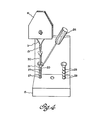
- the wire ends are removed, clustered or grouped together (if desired) inserted into a mold, and are thereafter reinserted into the solder bath. Suitable molds are shown in Figures 2 and 4 which are more completely discussed below.
- the mold, now filled with solder is removed and placed in a chill stand for cooling. Once the solder has solidified, the mold is removed thus releasing solid reliable superconductive joint which is typically between one and two inches in length. Additionally, it is also possible to impart a twist to the wire filaments following their removal from the superconductive solder bath and prior to their insertion into the mold.
- the method of superconductive joint manufacture of the present invention provides a rigid and reliable super- conductive joint which is significantly less prone to quench occurrences. It should also be appreciated that the method of the present invention is readily automatable, the use of the mold resulting in uniform and reliable superconductive joints whose manufacture does not depend upon the art or skill of manual assembly. Accordingly, the method of the present invention produces superconductive joints, solenoids, windings and general superconductive circuits which exhibit improved reliability and uniformity.
Landscapes
- Superconductors And Manufacturing Methods Therefor (AREA)
- Manufacturing Of Electrical Connectors (AREA)
Applications Claiming Priority (2)
| Application Number | Priority Date | Filing Date | Title |
|---|---|---|---|
| US678443 | 1984-12-05 | ||
| US06/678,443 US4713878A (en) | 1984-12-05 | 1984-12-05 | Mold method for superconductive joint fabrication |
Publications (3)
| Publication Number | Publication Date |
|---|---|
| EP0184184A2 true EP0184184A2 (de) | 1986-06-11 |
| EP0184184A3 EP0184184A3 (de) | 1988-12-07 |
| EP0184184B1 EP0184184B1 (de) | 2000-05-17 |
Family
ID=24722814
Family Applications (1)
| Application Number | Title | Priority Date | Filing Date |
|---|---|---|---|
| EP85115306A Expired - Lifetime EP0184184B1 (de) | 1984-12-05 | 1985-12-03 | Verfahren zum Herstellen einer supraleitenden Verbindung in einer Form |
Country Status (6)
| Country | Link |
|---|---|
| US (1) | US4713878A (de) |
| EP (1) | EP0184184B1 (de) |
| JP (1) | JPS61153987A (de) |
| CA (1) | CA1249039A (de) |
| DE (1) | DE3588223T2 (de) |
| IL (1) | IL77120A (de) |
Cited By (5)
| Publication number | Priority date | Publication date | Assignee | Title |
|---|---|---|---|---|
| EP0328903A3 (de) * | 1988-02-17 | 1989-11-15 | General Electric Company | Methode und Apparat zur Herstellung supraleitender Verbindungen |
| DE4102891A1 (de) * | 1991-01-31 | 1992-08-06 | Siemens Ag | Loetbare, supraleitende leitung und verwendung der leitung |
| US6975560B2 (en) | 2002-03-27 | 2005-12-13 | Bp Corporation North America Inc. | Geophysical method and apparatus |
| WO2018206982A1 (en) * | 2017-05-12 | 2018-11-15 | Oxford Instruments Nanotechnology Tools Limited | Method of joining a niobium titanium alloy by using an active solder |
| CN112134120A (zh) * | 2020-10-20 | 2020-12-25 | 中国科学院合肥物质科学研究院 | 一种rebco螺管型内插磁体接头端子的制作装置 |
Families Citing this family (5)
| Publication number | Priority date | Publication date | Assignee | Title |
|---|---|---|---|---|
| US5134040A (en) * | 1990-08-01 | 1992-07-28 | General Electric Company | Melt formed superconducting joint between superconducting tapes |
| JP2001155566A (ja) * | 1999-12-01 | 2001-06-08 | Internatl Superconductivity Technology Center | 超電導体の接合方法及び超電導体接合部材 |
| CA2721791C (en) * | 2008-04-17 | 2016-07-12 | Asg Superconductors S.P.A. | Granular superconducting joint |
| GB2487926B (en) | 2011-02-08 | 2013-06-19 | Siemens Plc | Joints with very low resistance between superconducting wires and methods for making such joints |
| GB2574210B (en) * | 2018-05-30 | 2022-09-28 | Siemens Healthcare Ltd | Superconducting joints |
Family Cites Families (10)
| Publication number | Priority date | Publication date | Assignee | Title |
|---|---|---|---|---|
| US2615074A (en) * | 1947-08-02 | 1952-10-21 | Gen Cable Corp | Cable pulling eye and method of making the same |
| US3169859A (en) * | 1962-03-27 | 1965-02-16 | Gen Electric | Superconductive materials |
| US3156539A (en) * | 1962-03-27 | 1964-11-10 | Gen Electric | Superconductive materials |
| US3422529A (en) * | 1963-12-09 | 1969-01-21 | North American Rockwell | Method of making a superconductive joint |
| US3346351A (en) * | 1964-12-17 | 1967-10-10 | Gen Electric | Superconductive connection |
| US3469020A (en) * | 1965-12-06 | 1969-09-23 | Kearney National Inc | Electrical spider connection |
| US3453378A (en) * | 1967-01-19 | 1969-07-01 | North American Rockwell | Superconductive joint |
| US3449818A (en) * | 1967-05-16 | 1969-06-17 | North American Rockwell | Superconductor joint |
| US3507949A (en) * | 1968-06-11 | 1970-04-21 | British Ropes Ltd | Method of socketing strands |
| US4584547A (en) * | 1983-12-30 | 1986-04-22 | General Electric Company | Superconducting joint for superconducting wires and coils |
-
1984
- 1984-12-05 US US06/678,443 patent/US4713878A/en not_active Expired - Lifetime
-
1985
- 1985-11-21 IL IL77120A patent/IL77120A/xx not_active IP Right Cessation
- 1985-11-29 CA CA000496576A patent/CA1249039A/en not_active Expired
- 1985-12-03 EP EP85115306A patent/EP0184184B1/de not_active Expired - Lifetime
- 1985-12-03 DE DE3588223T patent/DE3588223T2/de not_active Expired - Fee Related
- 1985-12-04 JP JP60271720A patent/JPS61153987A/ja active Granted
Cited By (8)
| Publication number | Priority date | Publication date | Assignee | Title |
|---|---|---|---|---|
| EP0328903A3 (de) * | 1988-02-17 | 1989-11-15 | General Electric Company | Methode und Apparat zur Herstellung supraleitender Verbindungen |
| US4901429A (en) * | 1988-02-17 | 1990-02-20 | General Electric Company | Method and apparatus for making a superconducting joint |
| DE4102891A1 (de) * | 1991-01-31 | 1992-08-06 | Siemens Ag | Loetbare, supraleitende leitung und verwendung der leitung |
| EP0497183A3 (de) * | 1991-01-31 | 1992-12-30 | Siemens Aktiengesellschaft | Lötbare, supraleitende Leitung und Verwendung der Leitung |
| US6975560B2 (en) | 2002-03-27 | 2005-12-13 | Bp Corporation North America Inc. | Geophysical method and apparatus |
| WO2018206982A1 (en) * | 2017-05-12 | 2018-11-15 | Oxford Instruments Nanotechnology Tools Limited | Method of joining a niobium titanium alloy by using an active solder |
| CN112134120A (zh) * | 2020-10-20 | 2020-12-25 | 中国科学院合肥物质科学研究院 | 一种rebco螺管型内插磁体接头端子的制作装置 |
| CN112134120B (zh) * | 2020-10-20 | 2021-09-17 | 中国科学院合肥物质科学研究院 | 一种rebco螺管型内插磁体接头端子的制作装置 |
Also Published As
| Publication number | Publication date |
|---|---|
| DE3588223D1 (de) | 2000-10-05 |
| IL77120A0 (en) | 1986-04-29 |
| CA1249039A (en) | 1989-01-17 |
| US4713878A (en) | 1987-12-22 |
| EP0184184B1 (de) | 2000-05-17 |
| EP0184184A3 (de) | 1988-12-07 |
| JPS61153987A (ja) | 1986-07-12 |
| IL77120A (en) | 1987-10-30 |
| JPH0365638B2 (de) | 1991-10-14 |
| DE3588223T2 (de) | 2001-02-15 |
Similar Documents
| Publication | Publication Date | Title |
|---|---|---|
| EP0148479B1 (de) | Verfahren zur Herstellung von Supraleitenden Verbindungen für supraleitende Drähte und Spulen | |
| US4148129A (en) | Aluminum-stabilized multifilamentary superconductor and method of its manufacture | |
| EP0073128B1 (de) | Supraleitender Verbunddraht | |
| JP4391403B2 (ja) | 二ホウ化マグネシウム超電導線の接続構造及びその接続方法 | |
| US4713878A (en) | Mold method for superconductive joint fabrication | |
| US4378330A (en) | Ductile alloy and process for preparing composite superconducting wire | |
| US3158794A (en) | Superconductive device | |
| EP0285147B1 (de) | Stromführende Leitung | |
| US20030207765A1 (en) | Method for fabricating a metal-clad superconductive body, and article comprising body | |
| Koike et al. | Fabrication of multifilament Nb3Sn conductors | |
| RU2134462C1 (ru) | Способ получения сверхпроводника на основе соединения nb3sn | |
| Otubo et al. | Submicron multifilamentary high performance Nb3Sn produced by powder metallurgy processing of large powders | |
| US3437459A (en) | Composite superconductor having a core of superconductivity metal with a nonsuperconductive coat | |
| Fietz et al. | Multifilamentary Nb 3 Sn conductor for fusion research magnets | |
| Cheggour et al. | Enhancement of the critical current density in Chevrel phase superconducting wires | |
| JPH09283253A (ja) | 超電導線材の超電導接続方法および超電導接続構造 | |
| Spencer et al. | Production of Nb 3 Sn by the in-situ process | |
| Young et al. | Fabrication and properties of an aluminum-stabilized nbti multifilament superconductor | |
| Yamada | Bi-based bulk current leads and their applications | |
| CA1036338A (en) | Method and apparatus for the manufacture of a superconductor | |
| Suenaga et al. | Effects of temperature ramp rate during heat treatment on hysteresis loss and critical current density of internal tin processed wires | |
| Zhang et al. | Tin core processing of powder metallurgy Cu-Nb-Sn | |
| Pasztor et al. | Development of Nb3Sn Cabled Conductor by External Diffusion Process and the Effect of Strain on the Critical Current | |
| Zhang et al. | Representation of A15 composition and TC in internal-Sn Nb3Sn superconducting strands | |
| Yu et al. | A new technique to fabricate multifilament Nb3Sn superconductor using cabled monocore subelements |
Legal Events
| Date | Code | Title | Description |
|---|---|---|---|
| PUAI | Public reference made under article 153(3) epc to a published international application that has entered the european phase |
Free format text: ORIGINAL CODE: 0009012 |
|
| AK | Designated contracting states |
Kind code of ref document: A2 Designated state(s): CH DE FR GB IT LI NL SE |
|
| PUAL | Search report despatched |
Free format text: ORIGINAL CODE: 0009013 |
|
| AK | Designated contracting states |
Kind code of ref document: A3 Designated state(s): CH DE FR GB IT LI NL SE |
|
| 17P | Request for examination filed |
Effective date: 19890520 |
|
| 17Q | First examination report despatched |
Effective date: 19910312 |
|
| GRAG | Despatch of communication of intention to grant |
Free format text: ORIGINAL CODE: EPIDOS AGRA |
|
| GRAG | Despatch of communication of intention to grant |
Free format text: ORIGINAL CODE: EPIDOS AGRA |
|
| GRAH | Despatch of communication of intention to grant a patent |
Free format text: ORIGINAL CODE: EPIDOS IGRA |
|
| GRAH | Despatch of communication of intention to grant a patent |
Free format text: ORIGINAL CODE: EPIDOS IGRA |
|
| GRAA | (expected) grant |
Free format text: ORIGINAL CODE: 0009210 |
|
| AK | Designated contracting states |
Kind code of ref document: B1 Designated state(s): CH DE FR GB IT LI NL SE |
|
| PG25 | Lapsed in a contracting state [announced via postgrant information from national office to epo] |
Ref country code: LI Free format text: LAPSE BECAUSE OF FAILURE TO SUBMIT A TRANSLATION OF THE DESCRIPTION OR TO PAY THE FEE WITHIN THE PRESCRIBED TIME-LIMIT Effective date: 20000517 Ref country code: IT Free format text: LAPSE BECAUSE OF FAILURE TO SUBMIT A TRANSLATION OF THE DESCRIPTION OR TO PAY THE FEE WITHIN THE PRESCRIBED TIME-LIMIT;WARNING: LAPSES OF ITALIAN PATENTS WITH EFFECTIVE DATE BEFORE 2007 MAY HAVE OCCURRED AT ANY TIME BEFORE 2007. THE CORRECT EFFECTIVE DATE MAY BE DIFFERENT FROM THE ONE RECORDED. Effective date: 20000517 Ref country code: FR Free format text: LAPSE BECAUSE OF FAILURE TO SUBMIT A TRANSLATION OF THE DESCRIPTION OR TO PAY THE FEE WITHIN THE PRESCRIBED TIME-LIMIT Effective date: 20000517 Ref country code: CH Free format text: LAPSE BECAUSE OF FAILURE TO SUBMIT A TRANSLATION OF THE DESCRIPTION OR TO PAY THE FEE WITHIN THE PRESCRIBED TIME-LIMIT Effective date: 20000517 |
|
| REG | Reference to a national code |
Ref country code: CH Ref legal event code: EP |
|
| PG25 | Lapsed in a contracting state [announced via postgrant information from national office to epo] |
Ref country code: SE Free format text: LAPSE BECAUSE OF FAILURE TO SUBMIT A TRANSLATION OF THE DESCRIPTION OR TO PAY THE FEE WITHIN THE PRESCRIBED TIME-LIMIT Effective date: 20000817 |
|
| REF | Corresponds to: |
Ref document number: 3588223 Country of ref document: DE Date of ref document: 20001005 |
|
| EN | Fr: translation not filed | ||
| REG | Reference to a national code |
Ref country code: CH Ref legal event code: PL |
|
| PLBE | No opposition filed within time limit |
Free format text: ORIGINAL CODE: 0009261 |
|
| STAA | Information on the status of an ep patent application or granted ep patent |
Free format text: STATUS: NO OPPOSITION FILED WITHIN TIME LIMIT |
|
| 26N | No opposition filed | ||
| REG | Reference to a national code |
Ref country code: GB Ref legal event code: IF02 |
|
| PGFP | Annual fee paid to national office [announced via postgrant information from national office to epo] |
Ref country code: NL Payment date: 20031120 Year of fee payment: 19 |
|
| PGFP | Annual fee paid to national office [announced via postgrant information from national office to epo] |
Ref country code: GB Payment date: 20031126 Year of fee payment: 19 |
|
| PGFP | Annual fee paid to national office [announced via postgrant information from national office to epo] |
Ref country code: DE Payment date: 20040202 Year of fee payment: 19 |
|
| PG25 | Lapsed in a contracting state [announced via postgrant information from national office to epo] |
Ref country code: GB Free format text: LAPSE BECAUSE OF NON-PAYMENT OF DUE FEES Effective date: 20041203 |
|
| PG25 | Lapsed in a contracting state [announced via postgrant information from national office to epo] |
Ref country code: NL Free format text: LAPSE BECAUSE OF NON-PAYMENT OF DUE FEES Effective date: 20050701 Ref country code: DE Free format text: LAPSE BECAUSE OF NON-PAYMENT OF DUE FEES Effective date: 20050701 |
|
| GBPC | Gb: european patent ceased through non-payment of renewal fee |
Effective date: 20041203 |
|
| NLV4 | Nl: lapsed or anulled due to non-payment of the annual fee |
Effective date: 20050701 |