EP0184320A1 - Architecture pour bus de mémoire - Google Patents
Architecture pour bus de mémoire Download PDFInfo
- Publication number
- EP0184320A1 EP0184320A1 EP85307880A EP85307880A EP0184320A1 EP 0184320 A1 EP0184320 A1 EP 0184320A1 EP 85307880 A EP85307880 A EP 85307880A EP 85307880 A EP85307880 A EP 85307880A EP 0184320 A1 EP0184320 A1 EP 0184320A1
- Authority
- EP
- European Patent Office
- Prior art keywords
- microprocessor
- bus
- memory
- read
- addressable memory
- Prior art date
- Legal status (The legal status is an assumption and is not a legal conclusion. Google has not performed a legal analysis and makes no representation as to the accuracy of the status listed.)
- Granted
Links
Images


Classifications
-
- G—PHYSICS
- G06—COMPUTING OR CALCULATING; COUNTING
- G06F—ELECTRIC DIGITAL DATA PROCESSING
- G06F13/00—Interconnection of, or transfer of information or other signals between, memories, input/output devices or central processing units
- G06F13/14—Handling requests for interconnection or transfer
- G06F13/16—Handling requests for interconnection or transfer for access to memory bus
-
- G—PHYSICS
- G06—COMPUTING OR CALCULATING; COUNTING
- G06F—ELECTRIC DIGITAL DATA PROCESSING
- G06F13/00—Interconnection of, or transfer of information or other signals between, memories, input/output devices or central processing units
- G06F13/38—Information transfer, e.g. on bus
- G06F13/42—Bus transfer protocol, e.g. handshake; Synchronisation
- G06F13/4204—Bus transfer protocol, e.g. handshake; Synchronisation on a parallel bus
- G06F13/4234—Bus transfer protocol, e.g. handshake; Synchronisation on a parallel bus being a memory bus
- G06F13/4243—Bus transfer protocol, e.g. handshake; Synchronisation on a parallel bus being a memory bus with synchronous protocol
Definitions
- This invention relates to an electronic microprocessor system, and in particular to an improved performance memory bus architecture for a microprocessor system.
- microprocessors In the field of microprocessors, it is common to have various portions of a microprocessor-based system (such as the microprocessor itself, memory units, and interface circuits for coupling the system to storage units and communications circuits) interconnected by means of one or more communications busses.
- the prior art teaches various combinations of bus architectures, including separate buses for data, address, and control information.
- many microprocessor-based systems use a single integrated bus for data, address, and control information.
- the Intel Corporation has developed a unified bus architecture known by the trademark "Multibus" for microprocessor system communication.
- a standard unified bus architecture is that in certain applications where processing speed is of paramount importance (such as in real-time data processing applications), the unified bus architecture is too slow when fast data transfer between memory and the system microprocessor is desired.
- retaining a standard unified bus within the system is advantageous, in that it allows standard circuits and interfaces to be coupled to the microprocessor system.
- the present invention is used in conjunction with a standard unified bus, and improves the speed of operation between the system microprocessor and the system memory. This improved performance is achieved by providing a second, separate memory bus apart from the unified system bus but controllably connectable to the unified bus, and by anticipating READ and WRITE commands. A minimum of control signals are required for operation of the secondary memory bus, thus permitting improved processing performance for data transfers between the microprocessor and the system memory.
- the improved performance which is an object of the present invention is achieved by coupling the system memory of a microprocessor system to a separate memory bus, and selectively electrically coupling the memory bus to a standard unified system bus.
- the microprocessor may selectively communicate over the unified bus using the standard protocol of the unified bus.
- the microprocessor When high speed memory operation is desired, the microprocessor generates address information that is decodable only by the system memory units, and the microprocessor transfers data to or from the system memory over the memory bus using a modified data transfer protocol.
- This modified data transfer protocol permits higher speed data transfers than the standard protocol for the unified bus.
- separate circuitry is provided and coupled to the microprocessor, to anticipate in most circumstances of use the occurrence of READ or WRITE commands to the system memory. This anticipation results in a substantial savings of time over the prior art method.
- the circuitry shown in FIGURE 1 comprises a basic microprocessor-based system that can be coupled to a unified bus and to the inventive memory bus through physical interface connections (not shown) to which are connected address, data, and control lines, as further described below. Only the microprocessor board itself and one or more memory banks can be connected through the memory bus.
- the memory bus uses a 24-bit addressing scheme where the four most significant bits have been designated the "bank" address. These four bits are used to select one of fifteen memory banks, which may be selected one at a time by the appropriate bank address.
- a sixteenth bank address (denoted by the hexidecimal number "F") is reserved as memory accessible only over the unified bus connected to the microprocessor circuit board.
- FIGURE 1 is a block diagram of the improved performance memory bus architecture of the preferred embodiment of the present invention.
- the microprocessor 1 is coupled by means of a bidirectional local address/data bus 2 to an internal address latch 3, to an external address latch and driver 4, to a bidirectional data transceiver 5, and to a bank register circuit 6 (each number within the busses throughout FIGURE 1 designate the width of the bus at that point).
- the external address latch 4 has twenty-four lines of address output. Twenty of these address lines are derived directly from the microprocessor 1, and the remaining four address lines are derived from the bank register circuit 6. Twenty of these twenty-four address lines from the external address latch 4 are coupled by an address bus 22 to a unified bus address transceiver 7, which in turn is coupled to the address lines 8 of a standard unified bus interface 21. All twenty-four address lines of the address bus 22 coming from the external address latch 4 are coupled to an inventive memory bus interface 20.
- the bidirectional data transceiver 5 transmits or receives up to sixteen simultaneous bits of information.
- the data transceiver 5 is coupled by a data bus 11 to a unified bus data transceiver 9, which in turn is coupled to the data lines 10 of the unified bus interface 21.
- the output of the data transceiver 5 is also coupled to the inventive memory bus interface 20 through the data bus 11.
- the 16-bit wide data path of the memory bus may be used for 8-bit or 16-bit transfers in known fashion.
- the microprocessor 1 also has three status lines 13 that are connected to an Early READ/WRITE logic circuit 12 and to a unified bus arbitration and control circuit 17 (which may be, for example, an Intel Corporation 8288 bus control circuit in combination with an 8289 bus arbitration circuit).
- Control lines 19 (further described below) from the unified bus interface 21 connect to the arbitration and control circuit 17, and to the Early READ/WRITE logic circuit 12.
- Other control lines (further described below) from the arbitration and control circuit 17 are also connected to the Early READ/WRITE logic circuit 12.
- connections from the unified bus interface 21 to the memory bus interface 20 are through intermediate buffer circuits or transceivers that can be tristated if desired in accordance with known art.
- One signal line from the unified bus interface 21 is always physically connected to a corresponding signal line on the memory bus interface 20. This is the Byte High Enable signal line, BHEN, 16.
- FIGURE 1 Other connections between the various circuit elements are shown in FIGURE 1. Omitted for the sake of clarity are such items as clocking signals, power and ground, and tristate enable control lines, which may be in accordance with known art.
- FIGURES 2a and 2b show generalized timing diagrams of the protocols for a READ operation and a WRITE operation for a prior art unified bus.
- an XACK acknowledgement signal from the memory unit is asserted after the memory unit has completed its READ or WRITE cycle. This delay in asserting the XACK acknowledgment signal is eliminated by the present invention, and is one of the main advantages of the present invention.
- the improved memory bus architecture of the present invention permits two different types of memory operation: normal operation and direct memory access (“DMA”) operations.
- the microprocessor 1 is the "bus master", which controls the standard unified bus in known fashion until such time as another "bus master" subsystem requests control of the unified bus.
- the microprocessor 1 gives up control of the unified bus and opens a direct electrical channel between the unified bus interface 21 and the memory bus interface 20. This is the second mode of operation, the DMA condition.
- the microprocessor cannot access the system memory during this time, and must wait until the current bus master releases the unified bus and the microprocessor 1 again becomes the bus master of the unified bus.
- the microprocessor 1 can control both the memory bus and the unified bus.
- the microprocessor 1 may access either bus at any time without further arbitration to gain control over either bus.
- a READ or WRITE operation over the memory bus using the inventive protocol begins when a new address is latched into the external address latch 4 and is asserted over the address bus 11.
- Decoding circuitry in each memory bank coupled to the memory bus interface 20 immediately decodes this address to determine if the microprocessor 1 is selecting that memory bank for access.
- the status of the microprocessor 1 is determined by the Early READ/WRITE logic circuit 12 which decodes the status line 13 outputs of the microprocessor 1 to determine if the microprocessor 1 is reading or writing to memory.
- the Early READ/WRITE logic circuit 12 will generate either a memory write (MWT) signal 14 or a memory read (MRD) signal 15, and apply it to the memory bus interface 20.
- a Byte High Enable signal, BHEN 16 is generated as a combination of the zero address line output, A0, from internal address latch 3, and a control signal, BHE, generated in known fashion by the microprocessor 1.
- the BHEN signal 16 need be asserted only by the time an MRD or MWT signal has been applied to the memory bus interface 20.
- the memory bank When a memory bank receives an appropriate address, the BHEN signal, and an MRD or MWT command, the memory bank responds back over the memory bus interface 20 with a RAM acknowledgement signal, RACK, to signal the microprocessor 1 that the memory bank will be ready to complete the READ or WRITE cycle.
- RACK RAM acknowledgement signal
- the RACK signal is synchronized with the microprocessor 1 system clock, which is also provided to the memory bus. Utilizing the master clock signal from the microprocessor circuit board, the selected memory bank operates synchronously with the microprocessor. This ensures maximum throughput during READ or WRITE operations.
- the RAM acknowledgment signal, RACK is only asserted long enough to be recognized by the microprocessor 1, which in the preferred embodiment is approximately 125 nanoseconds, or one clock period, and thus is asserted shortly after the MRD or MWT command line is asserted, as shown in FIGURES 3a and 3b.
- the XACK acknowledgment signal is not asserted until after a READ or WRITE operation has been completed.
- the microprocessor 1 receives an early acknowledgment that the READ or WRITE operation has commenced. That is, the RACK signal is generated a fixed time prior to the completion of the READ or WRITE operation. Therefore the microprocessor 1 can be (and is) programmed to respond on the assumption that the operation will finish, and thus the next cycle can be started. This anticipation typically saves one or two time periods, or "wait" states, compared to the prior art.
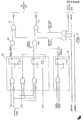
- the Early READ/WRITE logic circuit 12 shown in FIGURE 4 essentially is simple, combinatorial logic that very rapidly decodes the value of the status line 13 from the microprocessor 1 to generate Early READ or Early WRITE signals immediately after the status lines are valid.
- the logic elements in the area marked 40 generate the Early READ and Early WRITE signals. These signals are respectively logically OR'd with the standard READ command, BMRDC, and WRITE command, BMWCT, generated by the arbitration and control circuit 17 in known fashion.
- the generation of an Early READ signal is typically 100 nanoseconds before the arbitration and control circuit 17 asserts the standard BMRDC signal for a READ operation (called a "Delayed READ”).
- the generation of an Early WRITE signal is typically 160 nanoseconds before the assertion of the standard BMWCT signal for a WRITE operation (called a “Delayed WRITE”).
- the Early READ and Early WRITE signals save one clock period per memory bus cycle, which results in a 17% to 25% decrease in the time it takes to complete one memory bus cycle compared to cycles where a Delayed READ or Delayed WRITE signal is generated by the arbitration and control circuit 17.
- the logic elements in the area in FIGURE 4 marked 41 when enabled by a standard AENL signal generated by the arbitration and control circuit 17, monitors two of the standard unified bus arbitration and control signals, the common bus request, CBRQ, and the bus priority input signal, BPRNL.
- the AENL signal indicates that another subsystem is the bus master.
- the CBRQ signal indicates that another subsystem is requesting mastership of the unified bus.
- the BPRNL signal indicates whether a requesting subsystem has a higher priority than the present bus master.
- a HOLD-OFF signal is generated by the logic elements in the area marked 41 in FIGURE 4, which disables AND gates 42 and 43 and prevents the assertion of the Early READ or Early WRITE signals to the memory bus interface 20. If the arbitration and control circuit 17 resolves the bus mastership in favor of the microprocesser 1, the standard BMRDC or BMWCT signal from the arbitration and control circuit 17 is asserted through the Early READ/WRITE circuitry 12 to generate the respective MRD or MWT signal to the memory. If bus mastership is not resolved in favor of the microprocesser 1 during such a situation, then the DMA condition prevails.
- the address lines 8 of the unified bus interface 21 are therefore coupled through the address transciever 7 to twenty of the twenty-four address lines of the memory bus interface 20. (In some embodiments of the present invention, the address lines may be inverted first).
- the data lines 10 of the unified bus interface 21 are coupled through the unified bus data transciever 9 to the memory bus interface 20.
- the READ/WRITE command signals (MRDC and MWTD, respectively) from the unified bus are applied to the Early READ/WRITE logic circuit 12.
- the MRDC and MWTC commands from the unified bus are logically OR'd with the BMRDC and BMWTC signal lines, respectively, from the arbitration and control circuit 17, to also produce a Delayed READ or Delayed WRITE signal, which are then logically OR'd with the Early READ and Early WRITE signals to generate either the memory read signal, MRD 15, or the memory write signal, MWT 14, to the memory bus interface 20.
- the XACK acknowledgment signal and the standard unified bus protocol are used rather than the RACK acknowledgment signal protocol of the present invention.
- the timing of address, data, and control signals over the memory bus adheres to the unified bus protocol.
Landscapes
- Engineering & Computer Science (AREA)
- Theoretical Computer Science (AREA)
- Physics & Mathematics (AREA)
- General Engineering & Computer Science (AREA)
- General Physics & Mathematics (AREA)
- Bus Control (AREA)
- Complex Calculations (AREA)
- Microcomputers (AREA)
- Memory System (AREA)
Applications Claiming Priority (2)
| Application Number | Priority Date | Filing Date | Title |
|---|---|---|---|
| US66786584A | 1984-11-02 | 1984-11-02 | |
| US667865 | 1984-11-02 |
Publications (2)
| Publication Number | Publication Date |
|---|---|
| EP0184320A1 true EP0184320A1 (fr) | 1986-06-11 |
| EP0184320B1 EP0184320B1 (fr) | 1991-06-19 |
Family
ID=24679982
Family Applications (1)
| Application Number | Title | Priority Date | Filing Date |
|---|---|---|---|
| EP85307880A Expired - Lifetime EP0184320B1 (fr) | 1984-11-02 | 1985-10-31 | Architecture pour bus de mémoire |
Country Status (7)
| Country | Link |
|---|---|
| EP (1) | EP0184320B1 (fr) |
| JP (1) | JPS61166647A (fr) |
| KR (1) | KR920010977B1 (fr) |
| CA (1) | CA1238426A (fr) |
| DE (1) | DE3583283D1 (fr) |
| FI (1) | FI854317A7 (fr) |
| IE (1) | IE57399B1 (fr) |
Cited By (6)
| Publication number | Priority date | Publication date | Assignee | Title |
|---|---|---|---|---|
| EP0337537A1 (fr) * | 1988-04-05 | 1989-10-18 | Digital Equipment Corporation | Système de calculateur muni d'un bus principal et d'une ligne de communication supplémentaire reliée directement entre le processeur et la mémoire principale |
| EP0361142A3 (fr) * | 1988-09-29 | 1992-09-02 | Siemens Aktiengesellschaft | Bus standard universel |
| GB2256068A (en) * | 1991-05-21 | 1992-11-25 | Research Machines Plc | Bus cycle control |
| WO1993018451A1 (fr) * | 1992-03-06 | 1993-09-16 | Seiko Epson Corporation | Elimination du trajet critique dans les operations effectuees par les unites de commande de la memoire et des dispositifs d'entree/sortie |
| EP0709780A1 (fr) * | 1994-10-03 | 1996-05-01 | International Business Machines Corporation | Méthode et appareil pour reprise de transfer dans un système de traitement de données |
| WO2009081101A1 (fr) * | 2007-12-20 | 2009-07-02 | Symbian Software Limited | Procédé et système pour un accès à un dispositif périphérique amélioré |
Citations (3)
| Publication number | Priority date | Publication date | Assignee | Title |
|---|---|---|---|---|
| US4240138A (en) * | 1978-10-03 | 1980-12-16 | Texas Instruments Incorporated | System for direct access to a memory associated with a microprocessor |
| DE3007939A1 (de) * | 1980-03-01 | 1981-09-17 | Licentia Patent-Verwaltungs-Gmbh, 6000 Frankfurt | Anordnung zur kopplung von datenverarbeitungsanlagen |
| US4464715A (en) * | 1982-02-24 | 1984-08-07 | Daisy Systems Corporation | Memory accessing method |
-
1985
- 1985-10-31 EP EP85307880A patent/EP0184320B1/fr not_active Expired - Lifetime
- 1985-10-31 DE DE8585307880T patent/DE3583283D1/de not_active Expired - Fee Related
- 1985-11-01 KR KR1019850008152A patent/KR920010977B1/ko not_active Expired
- 1985-11-01 CA CA000494452A patent/CA1238426A/fr not_active Expired
- 1985-11-02 JP JP60246923A patent/JPS61166647A/ja active Pending
- 1985-11-04 IE IE2734/85A patent/IE57399B1/en unknown
- 1985-11-04 FI FI854317A patent/FI854317A7/fi not_active Application Discontinuation
Patent Citations (3)
| Publication number | Priority date | Publication date | Assignee | Title |
|---|---|---|---|---|
| US4240138A (en) * | 1978-10-03 | 1980-12-16 | Texas Instruments Incorporated | System for direct access to a memory associated with a microprocessor |
| DE3007939A1 (de) * | 1980-03-01 | 1981-09-17 | Licentia Patent-Verwaltungs-Gmbh, 6000 Frankfurt | Anordnung zur kopplung von datenverarbeitungsanlagen |
| US4464715A (en) * | 1982-02-24 | 1984-08-07 | Daisy Systems Corporation | Memory accessing method |
Non-Patent Citations (3)
| Title |
|---|
| COMPUTER DESIGN, vol. 21, no. 1, January 1982, pages 155-156,160,162,164, Winchester, Mass., US; J.P. ALTNETHER: "Better processor performance via global memory" * |
| CONFERENCE PROCEEDINGS-10TH ANNUAL INTERNATIONAL SYMPOSIUM ON COMPUTER ARCHITECTURE, 1983, Royal Institute of Technology, Stockholm, SE, pages 334-340, ACM, New York, US; L. PHILIPSON et al.: "A communication structure for a multiprocessor computer with distributed global memory" * |
| MICROPROCESSORS AND MICROSYSTEMS, vol. 6, no. 9, November 1982, pages 471-474, Butterworth & Co. (Publishers) Ltd., Whitstable, Kent, GB; R. BOBERG: "Major standardization issues of the proposed IEEE 796 bus - multibus" * |
Cited By (9)
| Publication number | Priority date | Publication date | Assignee | Title |
|---|---|---|---|---|
| EP0337537A1 (fr) * | 1988-04-05 | 1989-10-18 | Digital Equipment Corporation | Système de calculateur muni d'un bus principal et d'une ligne de communication supplémentaire reliée directement entre le processeur et la mémoire principale |
| EP0361142A3 (fr) * | 1988-09-29 | 1992-09-02 | Siemens Aktiengesellschaft | Bus standard universel |
| GB2256068A (en) * | 1991-05-21 | 1992-11-25 | Research Machines Plc | Bus cycle control |
| GB2256068B (en) * | 1991-05-21 | 1995-04-26 | Research Machines Plc | Bus cycle control means |
| WO1993018451A1 (fr) * | 1992-03-06 | 1993-09-16 | Seiko Epson Corporation | Elimination du trajet critique dans les operations effectuees par les unites de commande de la memoire et des dispositifs d'entree/sortie |
| US5828861A (en) * | 1992-03-06 | 1998-10-27 | Seiko Epson Corporation | System and method for reducing the critical path in memory control unit and input/output control unit operations |
| EP0709780A1 (fr) * | 1994-10-03 | 1996-05-01 | International Business Machines Corporation | Méthode et appareil pour reprise de transfer dans un système de traitement de données |
| US5623694A (en) * | 1994-10-03 | 1997-04-22 | International Business Machines Corporation | Aborting an I/O operation started before all system data is received by the I/O controller after detecting a remote retry operation |
| WO2009081101A1 (fr) * | 2007-12-20 | 2009-07-02 | Symbian Software Limited | Procédé et système pour un accès à un dispositif périphérique amélioré |
Also Published As
| Publication number | Publication date |
|---|---|
| KR860004359A (ko) | 1986-06-20 |
| FI854317A7 (fi) | 1986-05-03 |
| JPS61166647A (ja) | 1986-07-28 |
| EP0184320B1 (fr) | 1991-06-19 |
| DE3583283D1 (de) | 1991-07-25 |
| KR920010977B1 (ko) | 1992-12-26 |
| CA1238426A (fr) | 1988-06-21 |
| IE852734L (en) | 1986-05-02 |
| IE57399B1 (en) | 1992-08-26 |
| FI854317A0 (fi) | 1985-11-04 |
Similar Documents
| Publication | Publication Date | Title |
|---|---|---|
| US5448703A (en) | Method and apparatus for providing back-to-back data transfers in an information handling system having a multiplexed bus | |
| US5255374A (en) | Bus interface logic for computer system having dual bus architecture | |
| US5440751A (en) | Burst data transfer to single cycle data transfer conversion and strobe signal conversion | |
| US4449183A (en) | Arbitration scheme for a multiported shared functional device for use in multiprocessing systems | |
| US4757439A (en) | Memory bus architecture | |
| US3940743A (en) | Interconnecting unit for independently operable data processing systems | |
| US6516366B1 (en) | Serial bus for connecting two integrated circuits with storage for input/output signals | |
| US4999769A (en) | System with plural clocks for bidirectional information exchange between DMA controller and I/O devices via DMA bus | |
| US5379384A (en) | Configuration data loopback in a bus bridge circuit | |
| US6026464A (en) | Memory control system and method utilizing distributed memory controllers for multibank memory | |
| US5109490A (en) | Data transfer using bus address lines | |
| US5220651A (en) | Cpu-bus controller for accomplishing transfer operations between a controller and devices coupled to an input/output bus | |
| US4495564A (en) | Multi sub-channel adapter with single status/address register | |
| EP0492817A2 (fr) | Système de traitement de données et commande de mémoire pour des opérations de verrouillage de sémaphore | |
| US5987578A (en) | Pipelining to improve the interface of memory devices | |
| EP0627688A1 (fr) | Communication exact et complète entre architectures de bus différentes | |
| EP0030978B1 (fr) | Systeme de commande de transfert d'informations | |
| US5274784A (en) | Data transfer using bus address lines | |
| US6085261A (en) | Method and apparatus for burst protocol in a data processing system | |
| EP1109102B1 (fr) | Système mèmoire avec plusieurs dispositifs de mémoire et méthode d'accès en mémoire | |
| EP0784278B1 (fr) | Architecture d'interface pour raccordement avec un bus-PCI | |
| EP0184320B1 (fr) | Architecture pour bus de mémoire | |
| JP3108080B2 (ja) | アクセス制御回路装置 | |
| US6292867B1 (en) | Data processing system | |
| US5341501A (en) | Processor bus access |
Legal Events
| Date | Code | Title | Description |
|---|---|---|---|
| PUAI | Public reference made under article 153(3) epc to a published international application that has entered the european phase |
Free format text: ORIGINAL CODE: 0009012 |
|
| AK | Designated contracting states |
Kind code of ref document: A1 Designated state(s): DE FR GB IT NL SE |
|
| 17P | Request for examination filed |
Effective date: 19861128 |
|
| 17Q | First examination report despatched |
Effective date: 19880729 |
|
| GRAA | (expected) grant |
Free format text: ORIGINAL CODE: 0009210 |
|
| AK | Designated contracting states |
Kind code of ref document: B1 Designated state(s): DE FR GB IT NL SE |
|
| ITF | It: translation for a ep patent filed | ||
| REF | Corresponds to: |
Ref document number: 3583283 Country of ref document: DE Date of ref document: 19910725 |
|
| ET | Fr: translation filed | ||
| PLBE | No opposition filed within time limit |
Free format text: ORIGINAL CODE: 0009261 |
|
| STAA | Information on the status of an ep patent application or granted ep patent |
Free format text: STATUS: NO OPPOSITION FILED WITHIN TIME LIMIT |
|
| 26N | No opposition filed | ||
| PGFP | Annual fee paid to national office [announced via postgrant information from national office to epo] |
Ref country code: FR Payment date: 19930915 Year of fee payment: 9 |
|
| PGFP | Annual fee paid to national office [announced via postgrant information from national office to epo] |
Ref country code: DE Payment date: 19930916 Year of fee payment: 9 |
|
| PGFP | Annual fee paid to national office [announced via postgrant information from national office to epo] |
Ref country code: GB Payment date: 19930920 Year of fee payment: 9 |
|
| PGFP | Annual fee paid to national office [announced via postgrant information from national office to epo] |
Ref country code: SE Payment date: 19930921 Year of fee payment: 9 |
|
| PGFP | Annual fee paid to national office [announced via postgrant information from national office to epo] |
Ref country code: NL Payment date: 19931031 Year of fee payment: 9 |
|
| PG25 | Lapsed in a contracting state [announced via postgrant information from national office to epo] |
Ref country code: GB Effective date: 19941031 |
|
| PG25 | Lapsed in a contracting state [announced via postgrant information from national office to epo] |
Ref country code: SE Effective date: 19941101 |
|
| EAL | Se: european patent in force in sweden |
Ref document number: 85307880.6 |
|
| PG25 | Lapsed in a contracting state [announced via postgrant information from national office to epo] |
Ref country code: NL Effective date: 19950501 |
|
| NLV4 | Nl: lapsed or anulled due to non-payment of the annual fee | ||
| GBPC | Gb: european patent ceased through non-payment of renewal fee |
Effective date: 19941031 |
|
| PG25 | Lapsed in a contracting state [announced via postgrant information from national office to epo] |
Ref country code: FR Effective date: 19950630 |
|
| PG25 | Lapsed in a contracting state [announced via postgrant information from national office to epo] |
Ref country code: DE Effective date: 19950701 |
|
| EUG | Se: european patent has lapsed |
Ref document number: 85307880.6 |
|
| REG | Reference to a national code |
Ref country code: FR Ref legal event code: ST |