EP0184645A2 - Varistance en forme de puce et procédé de fabrication - Google Patents
Varistance en forme de puce et procédé de fabrication Download PDFInfo
- Publication number
- EP0184645A2 EP0184645A2 EP85113401A EP85113401A EP0184645A2 EP 0184645 A2 EP0184645 A2 EP 0184645A2 EP 85113401 A EP85113401 A EP 85113401A EP 85113401 A EP85113401 A EP 85113401A EP 0184645 A2 EP0184645 A2 EP 0184645A2
- Authority
- EP
- European Patent Office
- Prior art keywords
- cuboid
- varistor
- metallization
- metallized
- chip
- Prior art date
- Legal status (The legal status is an assumption and is not a legal conclusion. Google has not performed a legal analysis and makes no representation as to the accuracy of the status listed.)
- Granted
Links
- 238000004519 manufacturing process Methods 0.000 title claims abstract description 9
- 238000001465 metallisation Methods 0.000 claims abstract description 19
- 239000000463 material Substances 0.000 claims abstract description 17
- 239000004020 conductor Substances 0.000 claims description 5
- 238000010521 absorption reaction Methods 0.000 abstract description 6
- 238000000034 method Methods 0.000 abstract description 5
- 239000010410 layer Substances 0.000 description 9
- PXHVJJICTQNCMI-UHFFFAOYSA-N Nickel Chemical compound [Ni] PXHVJJICTQNCMI-UHFFFAOYSA-N 0.000 description 2
- XLOMVQKBTHCTTD-UHFFFAOYSA-N Zinc monoxide Chemical compound [Zn]=O XLOMVQKBTHCTTD-UHFFFAOYSA-N 0.000 description 2
- 230000015572 biosynthetic process Effects 0.000 description 2
- 239000006096 absorbing agent Substances 0.000 description 1
- 239000000919 ceramic Substances 0.000 description 1
- 239000013078 crystal Substances 0.000 description 1
- 230000000694 effects Effects 0.000 description 1
- 238000002474 experimental method Methods 0.000 description 1
- 229910052759 nickel Inorganic materials 0.000 description 1
- 239000011224 oxide ceramic Substances 0.000 description 1
- 229910052574 oxide ceramic Inorganic materials 0.000 description 1
- 238000007747 plating Methods 0.000 description 1
- 239000011241 protective layer Substances 0.000 description 1
- HBMJWWWQQXIZIP-UHFFFAOYSA-N silicon carbide Chemical compound [Si+]#[C-] HBMJWWWQQXIZIP-UHFFFAOYSA-N 0.000 description 1
- 229910010271 silicon carbide Inorganic materials 0.000 description 1
- 229910052709 silver Inorganic materials 0.000 description 1
- 239000004332 silver Substances 0.000 description 1
- 239000000126 substance Substances 0.000 description 1
- 239000000758 substrate Substances 0.000 description 1
- 230000001052 transient effect Effects 0.000 description 1
- 239000011787 zinc oxide Substances 0.000 description 1
Images

Classifications
-
- H—ELECTRICITY
- H01—ELECTRIC ELEMENTS
- H01C—RESISTORS
- H01C7/00—Non-adjustable resistors formed as one or more layers or coatings; Non-adjustable resistors made from powdered conducting material or powdered semi-conducting material with or without insulating material
- H01C7/10—Non-adjustable resistors formed as one or more layers or coatings; Non-adjustable resistors made from powdered conducting material or powdered semi-conducting material with or without insulating material voltage responsive, i.e. varistors
- H01C7/102—Varistor boundary, e.g. surface layers
Definitions
- the invention relates to a chip varistor, consisting of a cuboid body, which is at least partly made of varistor material and has at least two metallized connection surfaces on two opposite square ends, and a method for its production.
- Higher energy absorption values can be achieved by increasing the volume of the varistor, for example the entire body can be made of varistor material be formed. If the same contacting is used as in the known chip varistors, then there is a flashover on the varistor surface with higher pulse currents.
- This spark formation between the metallized pads at the ends of the cuboid body, which has dimensions of 8 x 4 x 2 mm, for example, is due to the fact that the contacting formed by the metallized pads favors a current flow on the surface of the varistor, while the inside of the varistor remains practically current free. At higher voltages or pulse currents above approximately 20 A, there is therefore overturning on the top and bottom sides of the varistor.
- the object of the invention is therefore to design the chip varistor of the type mentioned so that it has both a sufficient volume to obtain the required energy absorption capacity, as well as security against sliding sparks on its surface and also offers the possibility of its Make tension adjustable with constant dimensions of its top and bottom sides.
- the current flow direction is rotated by 90 ° so that current or voltage flashovers are only possible in the area of the interruption of the metallization.
- the adjustable speed of the varistor voltage is made possible in a simple manner that different dimensions are chosen for the thickness of the cuboid body, which is denoted by H in the exemplary embodiment.
- each strip-shaped recess can be delimited by two parallel edges which extend parallel to the edges of the top and bottom sides, transversely to the longitudinal direction of the cuboid body.
- the surface of the varistor material in the area of the strip-shaped recesses can be provided with grooves which are worked into the varistor material and extend in the direction of the strip-shaped recesses.
- the cuboid body as a laminated body, consisting of alternating layers of varistor material and electrically highly conductive material running parallel to its top and bottom sides, the latter layer in turn alternating with one and the other metallized Cuboid ends are electrically connected.
- a method is used, according to which a cuboid body is made of varistor material and is completely metallized on its surfaces, whereupon at least one each in the opposite top and bottom sides of the cuboid body Metallization-sparing groove is incorporated and then the body transverse to its longitudinal axis in individual longitudinal Pieces is cut, which form the actual cuboid body, so that its longitudinal axis runs in the direction of the transverse axis of the original cuboid body and its transverse axis in the direction of the longitudinal axis of the original cuboid body.
- the chip varistor shown in FIG. 1 is a cuboid body 1. Its dimensions are, for example, 2 x 1.25 x 0.5 mm (length, width, height) to, for example, 8 x 4 x 4 mm. It consists of an oxide-ceramic resistance material and is provided on the cuboid ends 2, 3 with metallized connection surfaces 8, 9, which completely cover the cuboid ends, and also on its top side 4 and its underside 5 with a metallization 6, 7 (FIG.
- the metallization of the upper side 4 is electrically conductively connected to the metallized connection surface 9 of one cuboid end 3, while the metallization 7 of the underside 5 is only electrically conductively connected to the metallized connection surface 8 of the other cuboid end 2.
- This means that the metallization is interrupted both on the upper side 4 and on the underside 5, this interruption, as can be seen in FIGS. 1 and 2, in each case forms a strip-shaped recess 10, 11 in the metallized surface which extends up to Surface of the varistor material ranges, which is generally designated 19.
- the strip-shaped recesses 10, 11 are delimited by two parallel edges 12, 13 which extend parallel to the edges of its upper and lower sides lying in the transverse direction of the body.
- This design of the chip varistor allows its voltage to be fixed at a constant "base area" of the cuboid body by changing the overall height H (FIG. 2), that is to say during the manufacture of the chip varistor lay. This means that the voltage can be adjusted depending on the component height.
- H overall height
- the width d of the strip-shaped recesses 10, 11 about the 1, 5 times the height H must be there after by this design due to the Oberlappung the electrode (metallized surface), the current flow to a only at the the front side of the cuboid ends contacted chip varistor is rotated by 90 °, the possibility of current or voltage flashovers is only given in the area of the strip-shaped recess.
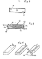
- FIG. 5 shows another embodiment of the chip varistor, in which the cuboid body is designed as a laminated body 16, consisting of a plurality of alternating layers of varistor material 17 and electrically highly conductive material 18 that run parallel to the top and bottom sides.
- the conductive material layers 18 are in turn alternately electrically connected to one and the other metallized cuboid ends 2a and 3a.
- the energy absorption capacity can still be increased significantly, but at the cost of a considerably higher manufacturing effort.
- a method is used to produce a chip varistor of the type shown in FIGS. 3 and 4, the steps of which are explained below with reference to FIGS. 6a, 6b and 6c.
- the surface of the chip varistor thus produced is, with the exception of the contact areas, i.e. the front ends, covered with a protective layer.
- the contact areas can be reinforced, for example, by nickel plating and tinning.
Landscapes
- Engineering & Computer Science (AREA)
- Microelectronics & Electronic Packaging (AREA)
- Physics & Mathematics (AREA)
- Electromagnetism (AREA)
- Thermistors And Varistors (AREA)
Priority Applications (1)
| Application Number | Priority Date | Filing Date | Title |
|---|---|---|---|
| AT85113401T ATE40765T1 (de) | 1984-12-14 | 1985-10-22 | Chip-varistor und verfahren zu seiner herstellung. |
Applications Claiming Priority (2)
| Application Number | Priority Date | Filing Date | Title |
|---|---|---|---|
| DE19843445698 DE3445698A1 (de) | 1984-12-14 | 1984-12-14 | Chip-varistor und verfahren zu seiner herstellung |
| DE3445698 | 1984-12-14 |
Publications (3)
| Publication Number | Publication Date |
|---|---|
| EP0184645A2 true EP0184645A2 (fr) | 1986-06-18 |
| EP0184645A3 EP0184645A3 (en) | 1987-01-28 |
| EP0184645B1 EP0184645B1 (fr) | 1989-02-08 |
Family
ID=6252820
Family Applications (1)
| Application Number | Title | Priority Date | Filing Date |
|---|---|---|---|
| EP85113401A Expired EP0184645B1 (fr) | 1984-12-14 | 1985-10-22 | Varistance en forme de puce et procédé de fabrication |
Country Status (3)
| Country | Link |
|---|---|
| EP (1) | EP0184645B1 (fr) |
| AT (1) | ATE40765T1 (fr) |
| DE (1) | DE3445698A1 (fr) |
Cited By (4)
| Publication number | Priority date | Publication date | Assignee | Title |
|---|---|---|---|---|
| GB2242066A (en) * | 1990-03-16 | 1991-09-18 | Ecco Ltd | Varistors |
| US5837178A (en) * | 1990-03-16 | 1998-11-17 | Ecco Limited | Method of manufacturing varistor precursors |
| US5973588A (en) * | 1990-06-26 | 1999-10-26 | Ecco Limited | Multilayer varistor with pin receiving apertures |
| US6183685B1 (en) | 1990-06-26 | 2001-02-06 | Littlefuse Inc. | Varistor manufacturing method |
Families Citing this family (3)
| Publication number | Priority date | Publication date | Assignee | Title |
|---|---|---|---|---|
| DE3731966C3 (de) * | 1986-09-26 | 1995-02-09 | Gen Electric | Oberflächenmontierbarer Varistor |
| DE4029681A1 (de) * | 1990-09-19 | 1992-04-02 | Siemens Ag | Verfahren zum herstellen von oberflaechenmontierbaren keramischen bauelementen in melf-technologie |
| DE102006033691A1 (de) | 2006-07-20 | 2008-01-31 | Epcos Ag | Widerstandselement mit PTC-Eigenschaften und hoher elektrischer und thermischer Leitfähigkeit |
Family Cites Families (8)
| Publication number | Priority date | Publication date | Assignee | Title |
|---|---|---|---|---|
| US2777039A (en) * | 1954-06-29 | 1957-01-08 | Standard Coil Prod Co Inc | Resistor elements adapted for use in connection with printed circuits |
| DE1064574B (de) * | 1956-02-04 | 1959-09-03 | Blaupunkt Werke Gmbh | Schaltungselement zur Verwendung in sogenannten gedruckten Schaltungen |
| AT237111B (de) * | 1961-12-27 | 1964-11-25 | Elettronica Metal Lux S P A | Verfahren zur Herstellung flacher, elektrischer Schaltelemente |
| DE2126340C3 (de) * | 1971-05-24 | 1973-10-25 | Matsushita Electric Industrial Co., Ltd., Kadoma, Osaka (Japan) | Mit Elektroden versehener Dick schichtwiderstand |
| US3768058A (en) * | 1971-07-22 | 1973-10-23 | Gen Electric | Metal oxide varistor with laterally spaced electrodes |
| JPS5823921B2 (ja) * | 1978-02-10 | 1983-05-18 | 日本電気株式会社 | 電圧非直線抵抗器 |
| DE3019969A1 (de) * | 1980-05-24 | 1981-12-03 | Philips Patentverwaltung Gmbh, 2000 Hamburg | Spannungsabhaengiger widerstand und verfahren zu seiner herstellung |
| ATE34482T1 (de) * | 1984-07-31 | 1988-06-15 | Siemens Bauelemente Ohg | Varistor in chip-bauweise zur verwendung in gedruckten schaltungen und verfahren zu seiner herstellung. |
-
1984
- 1984-12-14 DE DE19843445698 patent/DE3445698A1/de active Granted
-
1985
- 1985-10-22 AT AT85113401T patent/ATE40765T1/de not_active IP Right Cessation
- 1985-10-22 EP EP85113401A patent/EP0184645B1/fr not_active Expired
Cited By (7)
| Publication number | Priority date | Publication date | Assignee | Title |
|---|---|---|---|---|
| GB2242066A (en) * | 1990-03-16 | 1991-09-18 | Ecco Ltd | Varistors |
| GB2242066B (en) * | 1990-03-16 | 1994-04-27 | Ecco Ltd | Varistor structures |
| US5837178A (en) * | 1990-03-16 | 1998-11-17 | Ecco Limited | Method of manufacturing varistor precursors |
| US6334964B1 (en) | 1990-03-16 | 2002-01-01 | Littelfuse, Inc. | Varistor ink formulations |
| US6743381B2 (en) | 1990-03-16 | 2004-06-01 | Littlefuse, Inc. | Process for forming varistor ink composition |
| US5973588A (en) * | 1990-06-26 | 1999-10-26 | Ecco Limited | Multilayer varistor with pin receiving apertures |
| US6183685B1 (en) | 1990-06-26 | 2001-02-06 | Littlefuse Inc. | Varistor manufacturing method |
Also Published As
| Publication number | Publication date |
|---|---|
| ATE40765T1 (de) | 1989-02-15 |
| EP0184645A3 (en) | 1987-01-28 |
| DE3445698A1 (de) | 1986-06-26 |
| EP0184645B1 (fr) | 1989-02-08 |
| DE3445698C2 (fr) | 1991-01-03 |
Similar Documents
| Publication | Publication Date | Title |
|---|---|---|
| DE4008507C2 (de) | Laminiertes LC-Filter | |
| DE19806296B4 (de) | NTC-Thermistorelemente | |
| DE2235783C2 (de) | Metalloxid-Varistorelement | |
| EP2614508B1 (fr) | Composant résistance et procédé de fabrication d'un composant résistance | |
| DE3930000A1 (de) | Varistor in schichtbauweise | |
| DE1208368B (de) | Piezoelektrischer Kraftmesser | |
| DE19912851A1 (de) | Monolithischer Varistor | |
| EP0085980A1 (fr) | Résistance électrique de valeur ohmique basse, en particulier pour la protection contre la surcharge électrique d'un consommateur d'électricité | |
| DE10028014B4 (de) | Elektronisches Bauelement des Chiptyps | |
| DE2307322B2 (de) | Varistor | |
| EP0184645B1 (fr) | Varistance en forme de puce et procédé de fabrication | |
| DE1914442C3 (de) | Halbleiteranordnung | |
| DE2944069A1 (de) | Halbleiteranordnung | |
| DE3731967A1 (de) | Spannungsmultipliziervaristor | |
| DE1614858C3 (de) | Halbleiteranordnung | |
| DE1901452A1 (de) | Elektronisches Bauteil | |
| DE3905444C2 (de) | Keramischer Kondensator und Verfahren zu dessen Herstellung | |
| DE2437312C3 (de) | Verfahren zur Herstellung eines abgeglichenen Schichtwiderstandes | |
| DE112020005494T5 (de) | Varistor | |
| DE1097568B (de) | Verfahren zur Herstellung einer Halbleiteranordnung mit einem gleichmaessig gesinterten Koerper aus Erdalkalititanaten | |
| DE7320456U (de) | Elektrischer schichtwiderstand | |
| DE1950771C3 (de) | Verfahren zum Einstellen des Widerstand swertes für einen Schichtwiderstand | |
| DE2320482B2 (de) | Sperrschichtkondensator, Schaltungsanordnung von Sperrschichtkondensatoren und Verfahren zum Herstellen eines Sperrschichtkondensators | |
| EP0171642A1 (fr) | Varistance en forme de chip pour application dans les circuits imprimés et son procédé de fabrication | |
| DE2246573A1 (de) | Stapelkondensator |
Legal Events
| Date | Code | Title | Description |
|---|---|---|---|
| PUAI | Public reference made under article 153(3) epc to a published international application that has entered the european phase |
Free format text: ORIGINAL CODE: 0009012 |
|
| AK | Designated contracting states |
Kind code of ref document: A2 Designated state(s): AT BE FR NL |
|
| PUAL | Search report despatched |
Free format text: ORIGINAL CODE: 0009013 |
|
| AK | Designated contracting states |
Kind code of ref document: A3 Designated state(s): AT BE FR NL |
|
| 17P | Request for examination filed |
Effective date: 19870312 |
|
| 17Q | First examination report despatched |
Effective date: 19880706 |
|
| GRAA | (expected) grant |
Free format text: ORIGINAL CODE: 0009210 |
|
| AK | Designated contracting states |
Kind code of ref document: B1 Designated state(s): AT BE FR NL |
|
| REF | Corresponds to: |
Ref document number: 40765 Country of ref document: AT Date of ref document: 19890215 Kind code of ref document: T |
|
| ET | Fr: translation filed | ||
| PLBE | No opposition filed within time limit |
Free format text: ORIGINAL CODE: 0009261 |
|
| STAA | Information on the status of an ep patent application or granted ep patent |
Free format text: STATUS: NO OPPOSITION FILED WITHIN TIME LIMIT |
|
| 26N | No opposition filed | ||
| PGFP | Annual fee paid to national office [announced via postgrant information from national office to epo] |
Ref country code: AT Payment date: 19901030 Year of fee payment: 6 |
|
| PGFP | Annual fee paid to national office [announced via postgrant information from national office to epo] |
Ref country code: NL Payment date: 19901031 Year of fee payment: 6 |
|
| PGFP | Annual fee paid to national office [announced via postgrant information from national office to epo] |
Ref country code: BE Payment date: 19901113 Year of fee payment: 6 |
|
| PG25 | Lapsed in a contracting state [announced via postgrant information from national office to epo] |
Ref country code: AT Effective date: 19911022 |
|
| PG25 | Lapsed in a contracting state [announced via postgrant information from national office to epo] |
Ref country code: BE Effective date: 19911031 |
|
| BERE | Be: lapsed |
Owner name: C. CONRADTY NURNBERG G.M.B.H. & CO. K.G. Effective date: 19911031 |
|
| PG25 | Lapsed in a contracting state [announced via postgrant information from national office to epo] |
Ref country code: NL Effective date: 19920501 |
|
| NLV4 | Nl: lapsed or anulled due to non-payment of the annual fee | ||
| PGFP | Annual fee paid to national office [announced via postgrant information from national office to epo] |
Ref country code: FR Payment date: 19920930 Year of fee payment: 8 |
|
| PG25 | Lapsed in a contracting state [announced via postgrant information from national office to epo] |
Ref country code: FR Effective date: 19940630 |
|
| REG | Reference to a national code |
Ref country code: FR Ref legal event code: ST |