EP0184806A2 - Rechnermodule mit Datencode veränderlicher Wortlänge für Datenflussprozessor - Google Patents
Rechnermodule mit Datencode veränderlicher Wortlänge für Datenflussprozessor Download PDFInfo
- Publication number
- EP0184806A2 EP0184806A2 EP85115649A EP85115649A EP0184806A2 EP 0184806 A2 EP0184806 A2 EP 0184806A2 EP 85115649 A EP85115649 A EP 85115649A EP 85115649 A EP85115649 A EP 85115649A EP 0184806 A2 EP0184806 A2 EP 0184806A2
- Authority
- EP
- European Patent Office
- Prior art keywords
- wordlength
- full
- code
- codes
- indicator
- Prior art date
- Legal status (The legal status is an assumption and is not a legal conclusion. Google has not performed a legal analysis and makes no representation as to the accuracy of the status listed.)
- Withdrawn
Links
Images

Classifications
-
- G—PHYSICS
- G06—COMPUTING OR CALCULATING; COUNTING
- G06F—ELECTRIC DIGITAL DATA PROCESSING
- G06F9/00—Arrangements for program control, e.g. control units
- G06F9/06—Arrangements for program control, e.g. control units using stored programs, i.e. using an internal store of processing equipment to receive or retain programs
- G06F9/30—Arrangements for executing machine instructions, e.g. instruction decode
- G06F9/30145—Instruction analysis, e.g. decoding, instruction word fields
- G06F9/30149—Instruction analysis, e.g. decoding, instruction word fields of variable length instructions
-
- G—PHYSICS
- G06—COMPUTING OR CALCULATING; COUNTING
- G06F—ELECTRIC DIGITAL DATA PROCESSING
- G06F9/00—Arrangements for program control, e.g. control units
- G06F9/06—Arrangements for program control, e.g. control units using stored programs, i.e. using an internal store of processing equipment to receive or retain programs
- G06F9/44—Arrangements for executing specific programs
- G06F9/448—Execution paradigms, e.g. implementations of programming paradigms
- G06F9/4494—Execution paradigms, e.g. implementations of programming paradigms data driven
Definitions
- the present invention relates to computing modules for link-coupled dataflow processors.
- a plurality of computing modules are connected in a loop of common bus through which input and output data items are passed on from one module to another to effect necessary computations.
- Each data item comprises a select flag identifying a prescribed computing module and a variable identifying a data word contained in the data item.
- Each computing module includes a bus interface which decodes the select flag to determine whether the data item is to be passed on to the next computing module or whether it is destined for the own computing module.
- a queuing circuit is connected to the interface to receive the data word and its appending variable and stores the received data word until it receives a variable appending to a subsequent data word to be computed with the stored data word.
- the size and complexity of the computing module and hence the dataflow processor as a whole are determined by the maximum wordlength of the data to be handled by the system. Therefore, even if only one unit of the system requires the maximum wordlength, the other units must be capable of handling the same amount of data bits.
- This object is obtained by converting input data into a pair of codes of higher and lower significant bits, each having one-half the maximum wordlength of the system so that maximum wordlength data is divided into information bearing higher and lower significant bits of half-wordlength each and minimum wordlength data, which is one half the maximum wordlength, is converted to information bearing higher significant bits and all-zero containing lower significant bits of half-wordlength each.
- the present invention provides a computing module for a dataflow processor in which a variable wordlength code is converted into a series of first and second half-wordlength codes of higher and lower significant bits, respectively, and each half-wordlength code is appended by an identifying indicator.
- the module comprises a half-to-full word converter for sequentially receiving the half-wordlength codes and the indicators appending to them and combining the first and second half-wordlength codes into a full-wordlength code in response to the receipt of the indicator appending to the second half-wordlength code.
- a queuing circuit detects a full-wordlength code of later arrival from the half-to-full word converter which forms with a full-wordlength code of early arrival from the converter a data set necessary to effect computations and simultaneously sending the full-wordlength codes of early and later arrivals onto separate buses respectively.
- a computing logic effects the computations on the full-wordlength codes sent on the separate buses and produces a full-wordlength code indicating the result of the computations.
- a full-to-half word converter is included for dividing the full-wordlength code obtained by the computing logic into half-wordlength codes and appending an identifying indicator to each of the divided codes.
- the present invention provides an apparatus which comprises means connected in a common bus of a dataflow processor to receive a variable wordlength code for converting it into a series of first and second half-wordlength codes of higher and lower significant bits, respectively, and appending first and second indicators to each of the half-wordlength codes, the first indicator identifying a prescribed computing module and the second indicator identifying the half-wordlength code to which it appends.
- Each of the computing modules of the processor comprises an interface connected in the common bus for sequentially passing the first and second half-wordlength codes together with the appending first and second indicators to another computing module or sequentially passing the first and second half-wordlength codes together with the second indicators appending to the half-wordlength codes to the own computing module depending on the first indicator.
- a half-to-full word converter for sequentially receiving the half-wordlength codes and the second indicators appending to them from the interface and combining the first and second half-wordlength codes into a full-wordlength code in response to the receipt of the second indicator appending to the second half-wordlength code.
- a queuing circuit detects a full-wordlength code of later arrival from the half-to-full word converter which forms with a full-wordlength code of early arrival from the converter a data set necessary to effect computations and simultaneously sending the full-wordlength codes of early and later arrivals onto separate buses respectively.
- a computing logic effects the computations on the full-wordlength codes sent on the separate buses and produces a full-wordlength code indicating the result of the computations.
- a full-to-half word converter is provided for dividing the full-wordlength code obtained by the computing logic into half-wordlength codes and sequentially sending the divided codes to the interface and appending third and fourth indicators to each of the divided codes, the third and fourth indicators respectively identifying a prescribed computing module and each of the divided half-wordlength codes.
- the interface includes a multiplexer that sequentially receives the half-wordlength codes and the appending indicators from the full-to-half word converter to multiplex them with the half-wordlength codes and indicators which are to be passed on to another computing module.
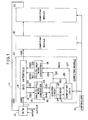
- a dataflow proccessor embodying the invention comprises a plurality of computing modules 10 connected successively in a common 48-line bus 11 which forms a loop. Each computing module 10 is under control of a controller 12 to effect intended computations. Input data is applied to an input-output circuit 13, known as "reader/writer" through which the data is applied to a specified computing module 10 and through which output data is withdrawn to an external circuit.
- reader/writer an input-output circuit
- the input data to the reader/writer 13 is of a variable length, either 64-bit full-wordlength or 32-bit half-wordlength. If the input data is of a full-wordlength, reader/writer 13 divides it into higher and lower significant bits of half wordlength each and generates an 8-bit select flag identifying a computing module in which the data is to be processed and a variable identifying each half-word data to form a data item as shown in Fig. 2. The data items are sequentially sent on bus 11 to a computing module 10. If the input data is of a half-wordlength, it is sent as higher significant bits followed by a half-word of 32 lower significant "0" bits.
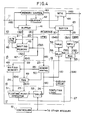
- Each computing module comprises a bus interface 14, a half-to-full word converter 15, a queuing circuit 16, a computing logic 17 and a full-to-half word converter 18.
- Bus interface 14 detects if the select flag appended to the input data specifies the own computing module and, if so, it sends the variable appended to it on an 8-line bus 20 and the received 32-bit word on a 32-line bus 21 to the half-to-full word converter 15. If the select flag specifies another computing module, the data item is passed to the next computing module.
- Half-to-full word converter 15 includes a memory in which the 32-bit data is stored.
- Converter 15 decodes the variable sent on bus 23 to detect when a subsequently arrived half-word data forms a full-word with the previous data stored in the memory. When this occurs, the higher and lower bit half-words are-combined together and sent on a 64-line bus 22 together with a variable indicating the 64-bit full-word data on an 8-line bus 23 to the queuing circuit. If the input data is of a half-wordlength, the converter 15 combines it with the following half-word of "0"s to form a 64-bit full word.
- Queuing circuit 16 includes a memory in which the full word data is stored until it receives a companion data word which forms a pair necessary to effect computations.
- the companion data words in pair are respectively sent on 64-line buses 24 and 25 to the computing logic 17 together with a variable indicating the pair sent on an 8-bit bus 26.
- Computing logic 17 performs computations as specified by the controller 12 and supplies the results of the computations on a 64-line bus 27 to the full-to-half word converter 18.
- Converter 18 divides the 64-bit computed data into half words of higher and lower significant bits and sends them sequentially on a 32-line bus 29 to the bus interface 14.
- the converter 18 receives the variable that identifies the computation data pair from queuing circuit 16 on a bus 28 to generate a variable identifying each of the divided half-word data, regenerates the select flag identifying the own computing module, and sends them on a 16-line bus 30 to the interface 14.
- Each of the half-wordlength data is sent on common bus 11 and passed on through the interfaces 14 of the subsequent computing modules 10 to the reader/writer 13 to be the output of the dataflow processor.
- the input data is applied to a 64-bit shift register 31. If the data has a 64-bit wordlength (double precision data), it is divided into half-words of higher and lower significant bits and respectively sent on 32-line buses 32 and 33 to a multiplexer 34. If the data is a 32-bit length word, it is stored in the higher bit positions of the shift register 31 and sent on bus 32 to the multiplexer 34 which receives a half-word of all zero bits on bus 33. Multiplexer 34 sequentially supplies the higher-and lower-bit half-word data to a 32-line bus 35.
- 64-bit wordlength double precision data
- the outputs of shift register 31 are applied to a table memory 36 which stores select flags and variables in locations addressable as a function of the data from shift register 31.
- a select flag and a variable are retrieved from the table memory 36 to be appended to each half-length word and sent on a 16-line bus 37 together with the data on bus 35 to the 48-line common bus 11.
- Reader/writer 13 includes a switching gate 38 which is responsive to a control signal from the controller 12 for switching the computed data to the output bus 39.
- the bus interface comprises a memory controller 40, first-in-first-out (FIFO) buffer memories 41, 42 and 43 and a multiplexer 44.
- the data item from reader/writer 13 is applied to buffer memories 41 and 42 and simultaneously stored therein, and also to the memory controller 40.
- Memory controller 40 decodes the select flag contained in the input data. If it specifies a computing module other than the own module, controller 40 enables the buffer 42 to pass the stored data item to the multiplexer 44 and thence to the common bus 11 multiplexed with the output of buffer 43. If the select flag specifies the own computing module, buffer 41 is enabled to pass the half-word data onto bus 21 and the variable identifying it onto bus 20.
- Half-to-full word converter 15 comprises a waiting memory 45 having a capacity of typically 256 x 32 bits and a read/write controller 46 which also includes a memory of 256 bits for storing read/write control bits and controls the read/write modes of the memory 45 in response to the variable sent from buffer 41.
- Waiting memory 45 is in a write mode when the variable identifying the higher-bit half-word data is received from buffer 41 and stores it in a location addressable as a function of the variable identifying it.
- Memory 45 is switched to a read mode in response to the variable identifying the lower-bit half-word data being received by read-write controller 46 and reads the stored higher-bit half-word data as a function of the last-mentioned variable.
- Memory 45 sends it onto an 32-line output bus 47, which is combined with the 32-line data input bus 21 to form a full-word on the 64-line bus 22.
- the full-word input data is recovered and the half-word input data is converted to a full-length word for double precision.
- Queuing circuit 16 includes a waiting memory 48, a 64-bit register 49 and a memory controller 50.
- the full-word data on bus 22 is input to the waiting memory 48 and to the register 49, and the variable identifying the full-word data is sent from buffer 41 on buses 20 and 23 to the memory controller 50.
- Memory controller 50 decodes the incoming variable in search of a subsequent companion data word neccessary to perform computations on the data stored in memory 48.
- controller 50 the companion data word has been stored in register 49, and proceeds to read the stored data out of the memory 48 onto bus 24 and sends a signal to the register 49 to transfer its contents onto bus 25.
- Computing logic 17 includes a floating point operator unit 51 which receives the companion data words on buses 24 and 25 to perform computations in accordance with the output of a table memory 52 which is in receipt of a variable sent on bus 26 from memory controller 50 indicating the pair of data words and an address from the controller 12.
- the result of the computations is sent on 64-line output bus 27 to the full-to-half word converter 18, which comprises a 64-bit shift register 53, a multiplexer 54, a delay 55 and a table memory 56.
- the output of floating point operator unit 51 is stored in the register 53 where it is divided into half-words of higher and lower bits and sent on 32-line buses 57 and 58 respectively to multiplexer 54.
- Multiplexer 54 sequentially sends the higher and lower bit half-words on bus 29 to buffer 43.
- Delay 55 is to introduce a delay time to the variable indicating the computed data so that it is time-coincident with it.
- Table memory 56 stores select flags and variables in locations addressable as a function of the variable sent from memory control 50. An 8-bit select flag and an 8-bit variable are read out of the memory 56 in response to the delayed variable applied thereto to be sent on bus 30 simultaneously with each half-word data output from multiplexer 54.
- Buffer memory 43 combines the half-word data with the select flag and variable to from an output data item in the same format as shown in Fig. 2 and sends it to multiplexer 44 to be multiplexed with the data delivered from buffer 42.
- the present invention provides an advantage in that if need arises to increase the maximum wordlength of an existing dataflow processor, it is only required to add a computing module of the invention to it, eliminating the need for altering the internal structure of the existing system.
- the computing module of the invention allows a compact design for dataflow processors. This is advantageous for use in aircraft where the processor is required to operate at high speeds and its weight and size are an important factor.
Landscapes
- Engineering & Computer Science (AREA)
- Software Systems (AREA)
- Theoretical Computer Science (AREA)
- Physics & Mathematics (AREA)
- General Engineering & Computer Science (AREA)
- General Physics & Mathematics (AREA)
- Multi Processors (AREA)
- Bus Control (AREA)
- Devices For Executing Special Programs (AREA)
Applications Claiming Priority (2)
| Application Number | Priority Date | Filing Date | Title |
|---|---|---|---|
| JP59260376A JPS61138333A (ja) | 1984-12-10 | 1984-12-10 | 演算モジユ−ル |
| JP260376/84 | 1984-12-10 |
Publications (2)
| Publication Number | Publication Date |
|---|---|
| EP0184806A2 true EP0184806A2 (de) | 1986-06-18 |
| EP0184806A3 EP0184806A3 (de) | 1987-10-28 |
Family
ID=17347062
Family Applications (1)
| Application Number | Title | Priority Date | Filing Date |
|---|---|---|---|
| EP85115649A Withdrawn EP0184806A3 (de) | 1984-12-10 | 1985-12-09 | Rechnermodule mit Datencode veränderlicher Wortlänge für Datenflussprozessor |
Country Status (3)
| Country | Link |
|---|---|
| EP (1) | EP0184806A3 (de) |
| JP (1) | JPS61138333A (de) |
| CA (1) | CA1258129A (de) |
Cited By (3)
| Publication number | Priority date | Publication date | Assignee | Title |
|---|---|---|---|---|
| EP0745932A3 (de) * | 1995-05-31 | 1998-09-09 | Matsushita Electric Industrial Co., Ltd. | Mikroprozessor zur Ausführung von Befehlen mit variablen Längen |
| FR2797962A1 (fr) * | 1999-08-23 | 2001-03-02 | Trusted Logic | Procede de conversion de types de variables codees dans un programme informatique et systeme de traduction de programme informatique correspondant |
| EP2104033A1 (de) | 2008-03-21 | 2009-09-23 | Fujitsu Limited | Verfahren und Prozessor zur Speicherung von Gleitkommadaten mit einfacher Genauigkeit |
Families Citing this family (1)
| Publication number | Priority date | Publication date | Assignee | Title |
|---|---|---|---|---|
| JPS62257536A (ja) * | 1986-04-30 | 1987-11-10 | Nec Corp | デ−タフロ−処理装置 |
Family Cites Families (4)
| Publication number | Priority date | Publication date | Assignee | Title |
|---|---|---|---|---|
| US4156903A (en) * | 1974-02-28 | 1979-05-29 | Burroughs Corporation | Data driven digital data processor |
| JPS55147737A (en) * | 1979-05-08 | 1980-11-17 | Nec Corp | Operation unit for variable pipe line |
| US4309754A (en) * | 1979-07-30 | 1982-01-05 | International Business Machines Corp. | Data interface mechanism for interfacing bit-parallel data buses of different bit width |
| JPS5987528A (ja) * | 1982-11-12 | 1984-05-21 | Fuji Electric Co Ltd | 連結デ−タの保証方式 |
-
1984
- 1984-12-10 JP JP59260376A patent/JPS61138333A/ja active Pending
-
1985
- 1985-12-09 CA CA000497195A patent/CA1258129A/en not_active Expired
- 1985-12-09 EP EP85115649A patent/EP0184806A3/de not_active Withdrawn
Cited By (6)
| Publication number | Priority date | Publication date | Assignee | Title |
|---|---|---|---|---|
| EP0745932A3 (de) * | 1995-05-31 | 1998-09-09 | Matsushita Electric Industrial Co., Ltd. | Mikroprozessor zur Ausführung von Befehlen mit variablen Längen |
| US5966514A (en) * | 1995-05-31 | 1999-10-12 | Matsushita Electric Industrial Co., Ltd. | Microprocessor for supporting reduction of program codes in size |
| US6253305B1 (en) | 1995-05-31 | 2001-06-26 | Matsushita Electric Industrial Co., Ltd. | Microprocessor for supporting reduction of program codes in size |
| FR2797962A1 (fr) * | 1999-08-23 | 2001-03-02 | Trusted Logic | Procede de conversion de types de variables codees dans un programme informatique et systeme de traduction de programme informatique correspondant |
| EP2104033A1 (de) | 2008-03-21 | 2009-09-23 | Fujitsu Limited | Verfahren und Prozessor zur Speicherung von Gleitkommadaten mit einfacher Genauigkeit |
| US8412761B2 (en) | 2008-03-21 | 2013-04-02 | Fujitsu Limited | Single precision floating-point data storing method and processor |
Also Published As
| Publication number | Publication date |
|---|---|
| EP0184806A3 (de) | 1987-10-28 |
| CA1258129A (en) | 1989-08-01 |
| JPS61138333A (ja) | 1986-06-25 |
Similar Documents
| Publication | Publication Date | Title |
|---|---|---|
| US5046000A (en) | Single-FIFO high speed combining switch | |
| EP0106670B1 (de) | Zentrale Verarbeitungseinrichtung mit mehreren Befehlsausführungseinheiten | |
| US5134702A (en) | Serial-to-parallel and parallel-to-serial converter | |
| US4750154A (en) | Memory alignment system and method | |
| US5347638A (en) | Method and apparatus for reloading microinstruction code to a SCSI sequencer | |
| US5592629A (en) | Apparatus and method for matching data rates to transfer data between two asynchronous devices | |
| EP0398523A2 (de) | Dateneingabe-/-ausgabevorrichtung und Ausführungsunterstützung in digitalen Prozessoren | |
| JPH07107676B2 (ja) | 順次通信制御装置 | |
| US5341506A (en) | Data flow processor with a full-to-half word convertor | |
| EP0126247B1 (de) | Rechnersystem | |
| HK36994A (en) | Apparatus for read handshake in high-speed asynchronous bus interface | |
| EP0184806A2 (de) | Rechnermodule mit Datencode veränderlicher Wortlänge für Datenflussprozessor | |
| US5146572A (en) | Multiple data format interface | |
| US5944788A (en) | Message transfer system and control method for multiple sending and receiving modules in a network supporting hardware and software emulated modules | |
| US4864491A (en) | Memory device | |
| EP0167959A2 (de) | Rechner-Vektorregisterverarbeitung | |
| US5748920A (en) | Transaction queue in a graphics controller chip | |
| US4528648A (en) | Memory management system | |
| US6301264B1 (en) | Asynchronous data conversion circuit | |
| US4737908A (en) | Buffer memory control system | |
| US5842003A (en) | Auxiliary message arbitrator for digital message transfer system in network of hardware modules | |
| US5115496A (en) | Queue device capable of quickly transferring a digital signal unit of a word length different from a single word length | |
| JP2908331B2 (ja) | リストベクトル処理システム | |
| US3805025A (en) | Document handling systems | |
| JPH0833869B2 (ja) | データ処理装置 |
Legal Events
| Date | Code | Title | Description |
|---|---|---|---|
| PUAI | Public reference made under article 153(3) epc to a published international application that has entered the european phase |
Free format text: ORIGINAL CODE: 0009012 |
|
| 17P | Request for examination filed |
Effective date: 19851209 |
|
| AK | Designated contracting states |
Kind code of ref document: A2 Designated state(s): DE FR GB IT NL |
|
| PUAL | Search report despatched |
Free format text: ORIGINAL CODE: 0009013 |
|
| AK | Designated contracting states |
Kind code of ref document: A3 Designated state(s): DE FR GB IT NL |
|
| 17Q | First examination report despatched |
Effective date: 19891027 |
|
| STAA | Information on the status of an ep patent application or granted ep patent |
Free format text: STATUS: THE APPLICATION IS DEEMED TO BE WITHDRAWN |
|
| 18D | Application deemed to be withdrawn |
Effective date: 19910207 |
|
| RIN1 | Information on inventor provided before grant (corrected) |
Inventor name: NAKADA, KATSUTOSHIC/O NEC CORPORATION Inventor name: NOHMI, HITOSHIC/O NEC CORPORATION |