EP0184859A2 - System zur Messung einer Elektronenstrahl-Linienbreite - Google Patents
System zur Messung einer Elektronenstrahl-Linienbreite Download PDFInfo
- Publication number
- EP0184859A2 EP0184859A2 EP85115938A EP85115938A EP0184859A2 EP 0184859 A2 EP0184859 A2 EP 0184859A2 EP 85115938 A EP85115938 A EP 85115938A EP 85115938 A EP85115938 A EP 85115938A EP 0184859 A2 EP0184859 A2 EP 0184859A2
- Authority
- EP
- European Patent Office
- Prior art keywords
- electron beam
- line width
- pattern
- electron
- secondary electrons
- Prior art date
- Legal status (The legal status is an assumption and is not a legal conclusion. Google has not performed a legal analysis and makes no representation as to the accuracy of the status listed.)
- Granted
Links
Images


Classifications
-
- H—ELECTRICITY
- H01—ELECTRIC ELEMENTS
- H01J—ELECTRIC DISCHARGE TUBES OR DISCHARGE LAMPS
- H01J37/00—Discharge tubes with provision for introducing objects or material to be exposed to the discharge, e.g. for the purpose of examination or processing thereof
- H01J37/26—Electron or ion microscopes; Electron or ion diffraction tubes
- H01J37/28—Electron or ion microscopes; Electron or ion diffraction tubes with scanning beams
-
- G—PHYSICS
- G01—MEASURING; TESTING
- G01B—MEASURING LENGTH, THICKNESS OR SIMILAR LINEAR DIMENSIONS; MEASURING ANGLES; MEASURING AREAS; MEASURING IRREGULARITIES OF SURFACES OR CONTOURS
- G01B15/00—Measuring arrangements characterised by the use of electromagnetic waves or particle radiation, e.g. by the use of microwaves, X-rays, gamma rays or electrons
-
- G—PHYSICS
- G01—MEASURING; TESTING
- G01B—MEASURING LENGTH, THICKNESS OR SIMILAR LINEAR DIMENSIONS; MEASURING ANGLES; MEASURING AREAS; MEASURING IRREGULARITIES OF SURFACES OR CONTOURS
- G01B7/00—Measuring arrangements characterised by the use of electric or magnetic techniques
- G01B7/02—Measuring arrangements characterised by the use of electric or magnetic techniques for measuring length, width or thickness
Definitions
- the present invention relates to an electron beam line width measurement system which measures the line width of a fine pattern such as wiring formed on the surface of a semiconductor substrate, by the use of an electron beam. More particularly, it relates to an electron beam line width measurement system which is well-suited to measure the line width of a pattern on a sample surface made of a plurality of different materials.
- the line width of the pattern is determined from only the signal corresponding to the amount of secondary electrons generated from the sample.
- the W gate 24 was thick enough to afford a good edge shape, and the sectional shape of the sample substrate was known, so that the edge signals could be read from the secondary electron signal.
- the conditions mentioned above are satisfied. Rather, it is common that there is no considerable difference between a secondary electron signal level corresponding to an Si substrate and a signal level corresponding to a W gate when the W gate is thinned more with rise in the integration density of an electron device.
- a sectional structure is usually unclear.
- the upper part 21 of Fig. 1 shows the sectional structure of the substrate; while the lower part 22 is a graph showing the amounts of secondary electrons versus the various positions of the sectional structure shown in the upper part 21.
- the secondary electron energy distribution of a semiconductor is narrower than that of a metal, and the secondary electron energy of the semiconductor at a position 35 at which the secondary electron emission yield ⁇ becomes the maximum is 2.5 - 5 eV, which are smaller than that of the metal being 5 - 10 eV at the corresponding position 36.
- curves 31, 32, 33 and 34 correspond to the secondary electrons of insulator materials encompassing semiconductors, the secondary electrons of metals, the reflected electrons of the insulator materials encompassing the semiconductors, and the reflected electrons of the metals, respectively.
- An object of the present invention is to eliminate the difficulties of the prior-art electron beam line width measurement system described above, and to provide an electron beam line width measurement system which detects, not only the stepped portion of a sample surface, but also the boundary defined by different substances, irrespective of the presence or absence of a level difference, whereby the line width of a pattern to be measured can be precisely evaluated.
- the present invention provides an electron beam line width measurement system wherein an electron beam is converged to a fine spot, the electron beam is scanned on a sample formed with a pattern to-be-measured, secondary electrons generated from a surface of the sample by the projection of the electron beam are detected, the relation between the intensity of the detected signal and a position irradiated with the"electron beam is found, and a line width of the pattern to-be-measured is determined from the relation, the system comprising a secondary electron detector which detects a signal corresponding to an amount of all secondary electrons generated by the scanning, and a secondary electron energy analyzer which selectively detects a signal corresponding to an amount of secondary electrons of specified energy.
- a signal processor for knowing the relation between the intensity of the secondary electron detection signal and the electron beam irradiation position which consists of an amplifier, an oscillograph etc. as required, is connected to the secondary electron detector and the secondary electron energy analyzer.
- the electron beam line width measurement system of the present invention comprises the secondary electron energy analyzer, the differences of the energy distribution of secondary electrons depending upon substances can be detected as information, and even a boundary in a sample surface defined by different substances can be detected irrespective of the presence or absence of a level difference.
- the system of the present invention can accordingly measure a pattern line width much more precisely than the prior art by combining the signal detection of the amount of secondary electrons from the stepped portion of a fine pattern, for example, formed on a semiconductor substrate and the detection of the difference of secondary, electron energy distributions based on different substances.
- the secondary electorn energy with which the maximum secondary electron emission yield is attained is 2.5 - 5 eV for semiconductors and 5 - 10 eV for metals. Therefore, when the system of the present invention is applied to a case where a metallic pattern exists on the surface of a semiconductor substrate, the position of the boundary of the substances can be separated and discriminated by detecting the amount of secondary electrons whose energies are, for example, near 10 eV or above about 10 eV. On the contrary, with the prior-art system exemplified in Fig. 1, the total number of secondary electrons of various energies is measured, and hence, the distinction based on substances as stated above is not reflected.
- a stepped pattern in a sample surface is measured by the secondary electron detector, a pattern formed of a different sort of substance is measured by the secondary electron energy analyzer, and a pattern having a level difference at the boundary between different sorts of substances is measured by the two.
- the secondary electron detector is necessary for the measurement of the stepped pattern made of an identical substance.
- the interaction between an electron beam and a substance is reflected upon the amount of secondary electrons and the energy distribution thereof, and especially, information specific to the substance is contained in the energy distribution of the secondary electrons.
- the prior-art pattern line width measurement employing an electron beam only the change of the amount of all secondary electrons from a substance making up a pattern is utilized, and hence, the detection of a substance difference has been unclear.
- the present invention measures the energy distribution of secondary electrons and detects also a signal specific to a substance, thereby making it possible to detect a pattern boundary even for a pattern having a small level difference at a step.
- the secondary electron detector and the secondary electron energy analyzer may be disposed likewise to the case of disposing the secondary electron detector in the prior-art electron beam line width measurement system. That is, they may be disposed at positions and with attitudes according to which they can receive secondary electrons.
- the scanning of the electron beam is done by moving the electron beam or the sample.
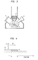
- Fig. 3 is a schematic view showing the arrangement of the electron beam line width measurement system of this embodiment
- Fig. 4 is an explanatory sectional view of a sample to-be-measured
- Fig. 5 is a diagram of the energy distributions of secondary electrons from the sample substrate and from a pattern (a thin metal film as an electrode) on the substrate
- Fig. 6 shows graphs of the relationships between the electron beam irradiation position of a sample surface and the amounts of detected secondary electrons, the upper part 13 of which has been obtained with a secondary electron detector 3 and the lower part 14 of which has been obtained with a secondary electron energy analyzer 4.
- symbols are common.
- an electron beam 1 is finely converged onto a sample to-be-measured 5 which is formed with a pattern to-be-measured.
- Secondary electrons 2 generated in consequence of the projection of the electron beam are detected by the secondary electron detector 3 and the secondary electron energy analyzer 4 so as to measure pattern positions on the basis of the signal fluctuations thereof.
- a scintillation counter having a photomultiplier was used as the secondary electron detector 3
- a cylindrical mirror analyzer (CMA) was used as the secondary electron energy analyzer 4.
- Numeral 7 in Fig. 3 designates a sample translation stage.
- a pattern to be measured is a thin metal film of an electrode 9 made of, e. g., W and formed on a semiconductor substrate 8 made of, e. g., Si and where the electron beam 1 is scanned in the direction of an arrow 12 as illustrated in Fig. 4.
- the step of the position b is detected from a detection signal corresponding to the amount of generation of secondary electrons (the prior art can obtain only this signal) as shown at 13 in Fig. 6, but the boundary cannot be detected at the position a if the difference of the secondary electron emission yields depending upon the substances is small.
- the energies of the secondary electrons are analyzed by the secondary electron energy analyzer 4 to obtain energy distribution curves, peaks and absorption specific to the substances are observed as shown in Fig. 5.
- a curve 10 is the energy distribution curve of the secondary electrons from the semiconductor substrate 8 in Fig. 4
- a broken-line curve 11 is the energy distribution curve of the secondary electrons from the thin metal film of the electrode 9 in Fig. 4.
- the secondary electron energy analyzer 4 is not restricted only to the CMA employed in this embodiment, but a measuring instrument in which a grid electrode to serve as an energy filter is disposed in front of a secondary electron detector can produce the same effect as that of the CMA as is well known.
- the secondary electron energy distribution curves of the respective materials constituting the surface of the smaple substrate are obtained to determine the energy value E A of the secondary electrons which are to be detected by the secondary electron energy analyzer, whereupon the electron beam is scanned on the sample surface to obtain the data of the amounts of detected secondary electrons at the respective positions as shown in Fig. 6.
- the materials constituting the sample surface are known in advance and where the secondary electron energy value E A is also known, the relations between the position of the sample surface and the amounts of detected secondary electrons as shown in Fig. 6 may be found by the use of the known value E A without obtaining the secondary electron energy distribution curves as shown in Fig. 5.
- a graph corresponding to the graph 13 in Fig. 6 obtained with the secondary electron detector 3 and a graph corresponding to the graph 14 in Fig. 6 obtained with the secondary electron energy analyzer 4 should desirably have the axes of abscissas indicative of positions taken in the same unit so that both the graphs can be readily compared with each other.
- the present invention it becomes possible to precisely detect a pattern boundary region defined by different sorts of materials in a stepped portion of a small level difference and accordingly to measure the line width of a pattern structure not having been measurable with the detection signal corresponding to the amount of generated secondary electrons in the prior-art method.
- the effect of the present invention is great for the reasons that each of most fine patterns in semiconductor processes is defined by a plurality of different substances, and that a pattern step becomes smaller and smaller with the microminiaturization of semiconductor devices.
Landscapes
- Physics & Mathematics (AREA)
- General Physics & Mathematics (AREA)
- Electromagnetism (AREA)
- Chemical & Material Sciences (AREA)
- Analytical Chemistry (AREA)
- Length-Measuring Devices Using Wave Or Particle Radiation (AREA)
- Testing Or Measuring Of Semiconductors Or The Like (AREA)
- Radar Systems Or Details Thereof (AREA)
Applications Claiming Priority (2)
| Application Number | Priority Date | Filing Date | Title |
|---|---|---|---|
| JP59262678A JPS61140811A (ja) | 1984-12-14 | 1984-12-14 | 電子ビ−ム測長装置 |
| JP262678/84 | 1984-12-14 |
Publications (3)
| Publication Number | Publication Date |
|---|---|
| EP0184859A2 true EP0184859A2 (de) | 1986-06-18 |
| EP0184859A3 EP0184859A3 (en) | 1987-08-12 |
| EP0184859B1 EP0184859B1 (de) | 1990-10-03 |
Family
ID=17379069
Family Applications (1)
| Application Number | Title | Priority Date | Filing Date |
|---|---|---|---|
| EP85115938A Expired - Lifetime EP0184859B1 (de) | 1984-12-14 | 1985-12-13 | System zur Messung einer Elektronenstrahl-Linienbreite |
Country Status (5)
| Country | Link |
|---|---|
| US (1) | US4740693A (de) |
| EP (1) | EP0184859B1 (de) |
| JP (1) | JPS61140811A (de) |
| KR (1) | KR940000735B1 (de) |
| DE (1) | DE3580004D1 (de) |
Families Citing this family (4)
| Publication number | Priority date | Publication date | Assignee | Title |
|---|---|---|---|---|
| JPH07122574B2 (ja) * | 1986-07-25 | 1995-12-25 | 株式会社日立製作所 | 断面形状測定方法 |
| US6511187B1 (en) | 1992-02-20 | 2003-01-28 | Kopin Corporation | Method of fabricating a matrix display system |
| US5876132A (en) * | 1995-05-23 | 1999-03-02 | International Business Machines Corporation | Method and system for high character density printing utilizing low pel density characters |
| JP2012068197A (ja) * | 2010-09-27 | 2012-04-05 | Toshiba Corp | 寸法測定方法および寸法測定装置ならびに寸法測定処理プログラム |
Family Cites Families (9)
| Publication number | Priority date | Publication date | Assignee | Title |
|---|---|---|---|---|
| AT279943B (de) * | 1965-07-14 | 1970-03-25 | Boehler & Co Ag Geb | Einrichtung zur Elektronenstrahl-Mikroanalyse heterogen aufgebauter metallischer oder nichtmetallischer Stoffe |
| US4139774A (en) * | 1977-02-09 | 1979-02-13 | Hitachi, Ltd. | Apparatus for irradiating a specimen by an electron beam |
| JPS53138790A (en) * | 1977-05-10 | 1978-12-04 | Nippon Steel Corp | Method and device for full electronic monitor |
| US4179604A (en) * | 1978-09-29 | 1979-12-18 | The United States Of America As Represented By The Secretary Of The Navy | Electron collector for forming low-loss electron images |
| JPS5572807A (en) * | 1978-11-27 | 1980-06-02 | Hitachi Ltd | Electron-beam mask check unit |
| JPS5796207A (en) * | 1980-12-05 | 1982-06-15 | Nec Corp | Measuring apparatus for pattern dimensions |
| JPS59112217A (ja) * | 1982-11-29 | 1984-06-28 | Toshiba Corp | 寸法測定方法 |
| JPS59163506A (ja) * | 1983-03-09 | 1984-09-14 | Hitachi Ltd | 電子ビ−ム測長装置 |
| JPS6033040A (ja) * | 1983-08-03 | 1985-02-20 | Hitachi Ltd | オ−ジエ電子分析装置 |
-
1984
- 1984-12-14 JP JP59262678A patent/JPS61140811A/ja active Granted
-
1985
- 1985-11-29 KR KR1019850008945A patent/KR940000735B1/ko not_active Expired - Fee Related
- 1985-12-11 US US06/807,681 patent/US4740693A/en not_active Expired - Fee Related
- 1985-12-13 EP EP85115938A patent/EP0184859B1/de not_active Expired - Lifetime
- 1985-12-13 DE DE8585115938T patent/DE3580004D1/de not_active Expired - Lifetime
Also Published As
| Publication number | Publication date |
|---|---|
| JPH0531724B2 (de) | 1993-05-13 |
| US4740693A (en) | 1988-04-26 |
| KR940000735B1 (ko) | 1994-01-28 |
| JPS61140811A (ja) | 1986-06-27 |
| KR860005207A (ko) | 1986-07-18 |
| EP0184859B1 (de) | 1990-10-03 |
| DE3580004D1 (de) | 1990-11-08 |
| EP0184859A3 (en) | 1987-08-12 |
Similar Documents
| Publication | Publication Date | Title |
|---|---|---|
| US5249216A (en) | Total reflection x-ray fluorescence apparatus | |
| US5220591A (en) | Total reflection X-ray fluorescence apparatus | |
| US5877498A (en) | Method and apparatus for X-ray analyses | |
| US6157032A (en) | Sample shape determination by measurement of surface slope with a scanning electron microscope | |
| JPH0731139B2 (ja) | 光感知性半導体材料からなる被検体表面層の無接触非破壊検査方法および検査装置 | |
| Graczyk et al. | Scanning electron diffraction attachment with electron energy filtering | |
| EP0158139A1 (de) | Fehlerkorrigierte Korpuskularstrahl-Lithographie | |
| US4740693A (en) | Electron beam pattern line width measurement system | |
| US5352894A (en) | Electron spectroscopy analyzer and a method of correcting a shift of spectral line in electron spectroscopy | |
| US5636256A (en) | Apparatus used for total reflection fluorescent X-ray analysis on a liquid drop-like sample containing very small amounts of impurities | |
| Balossier et al. | Parallel EELS elemental mapping in scanning transmission electron microscopy: use of the difference methods | |
| Russell et al. | Microchannel plate detector for low voltage scanning electron microscopes | |
| JPH08222172A (ja) | 電子顕微鏡 | |
| US6690010B1 (en) | Chemical analysis of defects using electron appearance spectroscopy | |
| JP2002139464A (ja) | 半導体装置の検査方法および検査装置 | |
| US7030375B1 (en) | Time of flight electron detector | |
| Rosenfield | Analysis of linewidth measurement techniques using the low voltage SEM | |
| US5804140A (en) | Corrosion inspection plate, measurement for corrosive environment and case for the corrosion inspection plate | |
| JPH08184678A (ja) | 荷電粒子ビームの寸法測定装置および測定方法 | |
| JPH07294460A (ja) | X線分析方法および装置 | |
| US6690009B1 (en) | Method of determining the charge carrier concentration in materials, notably semiconductors | |
| EP0247651B1 (de) | Elektronenstrahlprüfvorrichtung mit einer Prüfeinrichtung in der Form fingerartig ineinandergreifender elektrischer Leiter, sowie Methode zur Anwendung dieser Prüfschaltung | |
| JP2000055841A (ja) | X線分析方法 | |
| Mogami | Beam brightness modulation (BBM) method as applied to Auger electron spectroscopy | |
| SU1755144A1 (ru) | Способ рентгеноспектрального микроанализа твердых тел |
Legal Events
| Date | Code | Title | Description |
|---|---|---|---|
| PUAI | Public reference made under article 153(3) epc to a published international application that has entered the european phase |
Free format text: ORIGINAL CODE: 0009012 |
|
| AK | Designated contracting states |
Kind code of ref document: A2 Designated state(s): DE FR GB |
|
| PUAL | Search report despatched |
Free format text: ORIGINAL CODE: 0009013 |
|
| AK | Designated contracting states |
Kind code of ref document: A3 Designated state(s): DE FR GB |
|
| 17P | Request for examination filed |
Effective date: 19871223 |
|
| 17Q | First examination report despatched |
Effective date: 19890313 |
|
| GRAA | (expected) grant |
Free format text: ORIGINAL CODE: 0009210 |
|
| AK | Designated contracting states |
Kind code of ref document: B1 Designated state(s): DE FR GB |
|
| PG25 | Lapsed in a contracting state [announced via postgrant information from national office to epo] |
Ref country code: FR Effective date: 19901003 |
|
| REF | Corresponds to: |
Ref document number: 3580004 Country of ref document: DE Date of ref document: 19901108 |
|
| EN | Fr: translation not filed | ||
| PLBE | No opposition filed within time limit |
Free format text: ORIGINAL CODE: 0009261 |
|
| STAA | Information on the status of an ep patent application or granted ep patent |
Free format text: STATUS: NO OPPOSITION FILED WITHIN TIME LIMIT |
|
| 26N | No opposition filed | ||
| PGFP | Annual fee paid to national office [announced via postgrant information from national office to epo] |
Ref country code: GB Payment date: 19931203 Year of fee payment: 9 |
|
| PGFP | Annual fee paid to national office [announced via postgrant information from national office to epo] |
Ref country code: DE Payment date: 19940228 Year of fee payment: 9 |
|
| PG25 | Lapsed in a contracting state [announced via postgrant information from national office to epo] |
Ref country code: GB Effective date: 19941213 |
|
| GBPC | Gb: european patent ceased through non-payment of renewal fee |
Effective date: 19941213 |
|
| PG25 | Lapsed in a contracting state [announced via postgrant information from national office to epo] |
Ref country code: DE Effective date: 19950901 |