EP0184939A2 - Methode und Einrichtung zur Steuerung elektromagnetischer Geräte - Google Patents
Methode und Einrichtung zur Steuerung elektromagnetischer Geräte Download PDFInfo
- Publication number
- EP0184939A2 EP0184939A2 EP85309046A EP85309046A EP0184939A2 EP 0184939 A2 EP0184939 A2 EP 0184939A2 EP 85309046 A EP85309046 A EP 85309046A EP 85309046 A EP85309046 A EP 85309046A EP 0184939 A2 EP0184939 A2 EP 0184939A2
- Authority
- EP
- European Patent Office
- Prior art keywords
- coil
- solenoid coil
- current
- command signal
- energising
- Prior art date
- Legal status (The legal status is an assumption and is not a legal conclusion. Google has not performed a legal analysis and makes no representation as to the accuracy of the status listed.)
- Granted
Links
Images


Classifications
-
- H—ELECTRICITY
- H03—ELECTRONIC CIRCUITRY
- H03K—PULSE TECHNIQUE
- H03K17/00—Electronic switching or gating, i.e. not by contact-making and –breaking
- H03K17/04—Modifications for accelerating switching
- H03K17/041—Modifications for accelerating switching without feedback from the output circuit to the control circuit
- H03K17/0416—Modifications for accelerating switching without feedback from the output circuit to the control circuit by measures taken in the output circuit
- H03K17/04166—Modifications for accelerating switching without feedback from the output circuit to the control circuit by measures taken in the output circuit in bipolar transistor switches
-
- F—MECHANICAL ENGINEERING; LIGHTING; HEATING; WEAPONS; BLASTING
- F02—COMBUSTION ENGINES; HOT-GAS OR COMBUSTION-PRODUCT ENGINE PLANTS
- F02D—CONTROLLING COMBUSTION ENGINES
- F02D41/00—Electrical control of supply of combustible mixture or its constituents
- F02D41/20—Output circuits, e.g. for controlling currents in command coils
-
- H—ELECTRICITY
- H03—ELECTRONIC CIRCUITRY
- H03K—PULSE TECHNIQUE
- H03K17/00—Electronic switching or gating, i.e. not by contact-making and –breaking
- H03K17/51—Electronic switching or gating, i.e. not by contact-making and –breaking characterised by the components used
- H03K17/56—Electronic switching or gating, i.e. not by contact-making and –breaking characterised by the components used by the use, as active elements, of semiconductor devices
- H03K17/60—Electronic switching or gating, i.e. not by contact-making and –breaking characterised by the components used by the use, as active elements, of semiconductor devices the devices being bipolar transistors
- H03K17/64—Electronic switching or gating, i.e. not by contact-making and –breaking characterised by the components used by the use, as active elements, of semiconductor devices the devices being bipolar transistors having inductive loads
-
- F—MECHANICAL ENGINEERING; LIGHTING; HEATING; WEAPONS; BLASTING
- F02—COMBUSTION ENGINES; HOT-GAS OR COMBUSTION-PRODUCT ENGINE PLANTS
- F02D—CONTROLLING COMBUSTION ENGINES
- F02D41/00—Electrical control of supply of combustible mixture or its constituents
- F02D41/20—Output circuits, e.g. for controlling currents in command coils
- F02D2041/2003—Output circuits, e.g. for controlling currents in command coils using means for creating a boost voltage, i.e. generation or use of a voltage higher than the battery voltage, e.g. to speed up injector opening
- F02D2041/201—Output circuits, e.g. for controlling currents in command coils using means for creating a boost voltage, i.e. generation or use of a voltage higher than the battery voltage, e.g. to speed up injector opening by using a boost inductance
-
- F—MECHANICAL ENGINEERING; LIGHTING; HEATING; WEAPONS; BLASTING
- F02—COMBUSTION ENGINES; HOT-GAS OR COMBUSTION-PRODUCT ENGINE PLANTS
- F02D—CONTROLLING COMBUSTION ENGINES
- F02D41/00—Electrical control of supply of combustible mixture or its constituents
- F02D41/20—Output circuits, e.g. for controlling currents in command coils
- F02D2041/2017—Output circuits, e.g. for controlling currents in command coils using means for creating a boost current or using reference switching
-
- F—MECHANICAL ENGINEERING; LIGHTING; HEATING; WEAPONS; BLASTING
- F02—COMBUSTION ENGINES; HOT-GAS OR COMBUSTION-PRODUCT ENGINE PLANTS
- F02D—CONTROLLING COMBUSTION ENGINES
- F02D41/00—Electrical control of supply of combustible mixture or its constituents
- F02D41/20—Output circuits, e.g. for controlling currents in command coils
- F02D2041/202—Output circuits, e.g. for controlling currents in command coils characterised by the control of the circuit
- F02D2041/2024—Output circuits, e.g. for controlling currents in command coils characterised by the control of the circuit the control switching a load after time-on and time-off pulses
- F02D2041/2027—Control of the current by pulse width modulation or duty cycle control
-
- F—MECHANICAL ENGINEERING; LIGHTING; HEATING; WEAPONS; BLASTING
- F02—COMBUSTION ENGINES; HOT-GAS OR COMBUSTION-PRODUCT ENGINE PLANTS
- F02D—CONTROLLING COMBUSTION ENGINES
- F02D41/00—Electrical control of supply of combustible mixture or its constituents
- F02D41/20—Output circuits, e.g. for controlling currents in command coils
- F02D2041/202—Output circuits, e.g. for controlling currents in command coils characterised by the control of the circuit
- F02D2041/2031—Control of the current by means of delays or monostable multivibrators
-
- F—MECHANICAL ENGINEERING; LIGHTING; HEATING; WEAPONS; BLASTING
- F02—COMBUSTION ENGINES; HOT-GAS OR COMBUSTION-PRODUCT ENGINE PLANTS
- F02D—CONTROLLING COMBUSTION ENGINES
- F02D41/00—Electrical control of supply of combustible mixture or its constituents
- F02D41/20—Output circuits, e.g. for controlling currents in command coils
- F02D2041/202—Output circuits, e.g. for controlling currents in command coils characterised by the control of the circuit
- F02D2041/2041—Output circuits, e.g. for controlling currents in command coils characterised by the control of the circuit for controlling the current in the free-wheeling phase
Definitions
- the present invention relates to a method of, and a controller for, controlling electromagnet devices or actuators of the type comprising a body movable by the electromagnetic force of a solenoid coil.
- an actuator can be incorporated in an electromagnetic valve for accurate fuel injection in a diesel engine or an electromagnetic shut off valve, for example.
- a known form of controller operates switches of drive means to energise and de-energise a solenoid coil of an electromagnetic device in response to a command signal to cause a movable body be displaced between set positions.
- the known controller suffers from the disadvantage that it is not possible to energise and de-energise the solenoid coil rapidly because of the inductance of the coil.
- a general object of the present invention is to provide an improved form of contoller and a method of control to enhance the response of the electromagnetic device to changes in the command signal.
- the controller employs an additional coil which serves to store or absorb electromagnet energy and control means interconnects the coil to the solenoid coil in a manner to transfer energy from the coil to solenoid coil prior to the supply of energising current to the latter and/or to transfer energy from the solenoid coil to the other coil when the former is to be de-energised.
- the invention also provides a method of controlling an electromagnetic device of the type employing a solenoid coil operated by a command signal to cause a body to be displaced by energising the coil; said method comprising storing electromagnetic energy in another coil and transferring the electromagnetic energy stored in the other coil to the solenoid coil prior to the supply of energising current to the solenoid coil when the latter is to be re-energised by energising current to improve the response to the command signal requiring energisation of the solenoid coil. It is possible to further transfer electromagnetic energy from the solenoid coil to the other coil when the solenoid coil 'is to de-energised to improve the response to the command signal requiring de-energisation of the solenoid coil.
- the invention provides a method of controlling an electromagnetic device of the type employing a solenoid coil operated by a command signal to cause a body to be displaced by energising the coil; said method comprising utilising another coil and transferring electromagnetic energy from the solenoid coil to the other coil when the solenoid coil is to de-energised to improve the response to the command signal requiring de-energisation of the solenoid coil.
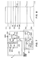
- FIG. 2 is a sectional view of a typical conventional electromagnetic device or actuator 1.
- the electromagnetic device 1 has, as basic structural elements, a plunger 2, which is a body movable in an axial direction, a solenoid coil SC wound around the plunger 2, a first yoke 4 and a second yoke 5.
- the plunger 2 is formed of a ferromagnetic material and is fixed to a shaft 6.
- Toward the outer end of the shaft 6 (the left end in Figure 2) is provided a bearing 7, and a complementary guide body 8 is provided for the plunger 2.
- the shaft 6 is fixed at the outer end to a return spring 9, and the other end of the return spring 9 is fixed in position.
- the right end of the plunger 2 is covered by a lid 10.
- the coil SC is connected in series with a switching transistor Q2 and a current detecting resistor Rl.
- a voltage E source is connected via a switching transistor Ql to the series circuit SC, Q2, Rl.
- a diode CR1 is connected across the series circuit SC, Q2, R1 with polarity opposite to the source E.
- a diode CR2 in series with a Zener diode ZD is connected across the coil SC and the polarity of the diode CR2 is the same as CR1.
- a comparator CM has inputs connected to the current detecting resistor R1 and to a current reference value holding current and an output connected to one input of an NOR-gate Glll.
- a timer TM111 receives a change-over command signal which determines the position of the movable body or plunger 2 and this command signal also feeds the base of the transistor Q2.
- the output of the timer TM111 feeds the other input of the NOR-gate G111 and the output of the NOR-gate Glll feeds the base of the transistor Ql.
- (1) is the energising command signal which commands whether or not the solenoid coil SC is to be energised
- (2) is the voltage waveform applied to the coil SC
- (3) is the waveform of the current flowing through coil SC
- (4) is the operating state of the transistor Ql
- (5) is the operating state of the transistor Q2.
- the energising command signal (1) goes from a low level to a high level the transistor Q2 is turned on, (5) and also the timer TM111 operates.
- the transistor Ql As shown in (4) for a set time interval Tl the transistor Ql is turned on, and current Ie flows in the direction of the solid line arrow A1 in Figure 11 from the direct current supply E through the transistor Q1, the solenoid coil SC, the transistor Q2 and the current detecting resistor Rl.
- the current Ie cannot, because of the inductance of the solenoid coil SC increase instantaneously but increase gradually with time t. If the voltage of the direct current supply E is Ve, and the direct current resistance of the solenoid coil SC is Rs, then the current Ie is given by:
- the solenoid coil SC is driven by the output of the comparator CM in chopper mode with the transistor Q1 undergoing repeated on/off operations and at a rated current of the holding current level IH.
- the current level Ie is detected by the current detecting resistor Rl, and when it grows larger than the holding current level IH the transistor Ql goes off and the current Ie flows through the diode CR1 and in the direction of the broken line arrow A2 in Figure 11 and decreases.
- this surge voltage VP is given by:
- the maximum surge voltage VP corresponding to the sum of the maximum Zener voltage VZ and the supply voltage Ve is applied to the transistor switch Q2. Therefore when the solenoid coil SC is de-energised the higher the Zener voltage VZ the faster it is de-energised, but also the higher the surge voltage VP.
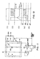
- Figure 1 depicts an improved form of controller.
- the electromagnetic or solenoid coil SC is in series with transistor switches Qll and Q12 and a current detecting resistor Rll and is connected directly to the source E.
- a further series circuit composed of a transistor Q13, a coil CC, an analog switch Q14 and a resistor R112 is also connected across the source E.
- a diode CR12 and a Zener diode ZD1 are connected across the coil SC.
- a diode CR11 is connected between the junction of the coil SC and the collector of the transistor Q11 on the one hand and the junction between the coil CC and the switch Q14 on the other hand.
- a diode CR13 is connected between the collector of the transistor Q13 and negative terminal of the source E.
- control means 20 composed of comparators CM11, CM12, timers TM11, TM12, edge detectors ED11, ED12 and various logic gates.
- the edge detector ED11 When the energising command signal is at a high level the edge detector ED11 provides a high level signal for the interval T3. When a high level signal is provided to the timer TM11 from the edge detector ED11, a high level signal is present at its output for the time interval Tl and is fed to input of an AND gate G12. When there is a rising or falling change in the energising command signal the edge detector ED12 outputs a high level signal for a time interval T4. The output signal of a NOR gate G17 controls the operation of the switch Q14. When the output is low the switch Q14 is off and when the output is high the switch is on.
- the output of the gate G17 is low for an interval T3 from a rising edge of the energising command signal and for an interval T4 from a falling edge.
- a high level signal is received by the timer TM12 from the edge detector ED12, a high level signal is applied for an interval T2 to one input of a NAND gate G13.
- the operation of the transistor Q12 is controlled by the output signal of a NAND gate G13. When the output signal of the gate G13 is high the transistor Q12 is turned on, and when low it is turned off.
- a voltage corresponding to a coil set current level ID for setting the current flowing through the coil SC is fed to the non-inverting input of a comparator CM11 having hysteresis characteristic with a hysteresis amplitude of I1.
- a voltage detected by the resistor R12 and corresponding to the current flowing in the coil CC is applied to the inverting input of the comparator CM11. This input is compared with the voltage corresponding to the current level ID.
- the output of the comparator CM11 is high, and when that voltage is lower the output of the comparator CM11 is low.
- the transistor Q13 is controlled by the output signal of a NAND gate 18, and when the output signal is low the transistor Q13 is turned on, and when low it is turned off.
- a voltage corresponding to a holding current level IH for setting the current flowing through the solenoid coil SC so that the holding state of the electromagnetic device 1 can be maintained is fed to the non-inverting input of the comparator CM12 having hysteresis characteristic with a hysteresis amplitude of ⁇ I2.
- the inverting input of the comparator CM12 receives the voltage detected by the resistor R11. When the voltage corresponding to the current level IH is higher the comparator CM12 has a high level output signal and when that voltage is lower the comparator CM12 has a low level output signal.
- Figure 3 illustrates the operation of the controller shown in Figure 1, showing the transistors Qll to Q13 and the analog switch Q14 as switches and showing the direction of current flow for the different on/off states of the switches Qll to Q14 while Figure 4 depicts the waveforms.
- Figure 4 (1) is the energising command signal
- (2) is the on/off state of the switch Q11
- (3) is the on/off state of the switch Q12
- (4) is the on/off state of the switch Q13
- (5) is the on/off state of the switch Q14
- (6) is the current waveform flowing through the coil CC
- (7) is the current waveform flowing through the solenoid coil SC.
- the current flowing in the coil CC will as shown in Fig. 4 fall instantaneously from the current level ID to the current level 10 shown in (4), and the current flowing in the solenoid coil SC will instantaneously rise to the same level.
- equation (1) the current in the solenoid coil SC rises with time t, but in the present invention, the energizing current of the solenoid coil SC is given an initial energizing value of a proportion of the current level ID of the coil CC immediately before energization corresponding to the inductance of the solenoid coil SC. The result is the time interval for the energizing current to rise can be made substantially shorter.
- an initial value of the energizing current of 1/2 of the current level ID of the coil CC is given by expression (4), and if the inductance of the solenoid coil SC is 1/2 of the inductance component of the coil CC, then an initial value of the energizing current of 2/3 of the current level ID will be obtained.
- the energizing current of the solenoid coil SC can be substantially increased.
- the switch Q14 After the switch Q14 has been off for an interval T3 as shown in Fig. 4 (5), the switch Q14 returns to the on state, and at the same time, as shown in Fig. 3 (4) the switch Q13 goes off, and the switch Qll goes on. At this time the current flowing in the coil CC will flow in the direction shown by arrow A14 through the diode CR13 and will decrease. On the other hand, the current flowing in the solenoid coil SC in the interval Tl which is slightly longer than the displacement time of the plunger 2 of the electromagnetic device 1 will flow as shown by the arrow A15 and will increase, and will become greater than the current level 10. Therefore in the present invention yet more speeding up of the movement of the plunger 2 can be obtained. At this point the current paths of the coil CC and the solenoid coil SC are cut off by the diode CR11.
- the current detection resistor Rll detects the current flowing in the solenoid coil SC and according to that detected current value, the switch Q11 turns on/off as shown in Fig. 4 (2), and the solenoid coil SC is driven in chopped mode with a rated current of the predetermined holding current level IH.
- the switch Qll when the switch Qll is off, the current flowing in the solenoid coil SC flows, as shown by the arrow A16 in Fig. 3 (5), in the closed circuit of switches Q12 and Q14 and diode CR11, and decreases.
- the back e.m.f. induced at both ends of the solenoid coil SC is low, there is hardly any current flow in the circuit of the Zener diode ZD1 and diode CR12.
- the current flowing in the solenoid coil SC falls from the holding current level IH to the current IC.
- the current falls instantaneously to 1/2 of IH if the inductance of the coil CC and the solenoid coil SC are equal, and to 1/3 of IH if the inductance of the latter is 1/2 of the inductance of the former.
- the switch Q12 goes off, the current flowing through the solenoid coil SC in the direction shown by the arrow A18 in Fig. 3 (7) through the closed circuit of the Zener diode ZD1 and diode CR12 decreases rapidly.
- the switch Q13 goes on again, the state of Fig. 3 (1) is returned to, and a current flows through the coil CC.
- the current Ie in Fig. 3 (7) flowing through the solenoid coil SC is given by the following:
- Figure 5 is an electrical circuit diagram showing another embodiment of a electromagnet controller in which the present invention is applied only when energising the solenoid coil.
- Figure 6 depicts the waveform associated with Figure 5.
- the transistors Q51, Q52 and Q53 are controlled by signals produced by control means 30.
- the energising command signal for ordering the energising of the solenoid coil SC is fed to an edge detector (ED) of the control means 30.
- the edge detector TED includes a timer.
- the command signal also feeds an inverter IN5 and is applied directly to the base of the transistor Q52.
- the edge detector TED including a timer applies a high output for the interval TS determined by the timer to one input of an OR gate G52.
- the inverter IN51 the command signal is inverted, and the output signal is applied to the base of the transistor Q53 and to the other input of the OR gate G52.
- the output signal of the OR gate G52 is applied to the base of transistor Q51.
- Figure 6 (1) is the energising command signal, (2) is the output signal of the AND gate G51 of the edge detector TED including the timer, (3) is the on/off state of the transistor Q51, (4) is the on/off state of the transistor Q52, (5) is the on/off state of the transistor Q53, (6) is the current waveform flowing through the coil CC, and (7) is the current waveform flowing through the solenoid coil SC.
- the transistors Q51 and Q52 are in the off state, the transistor Q53 is in the on state, and current is supplied in the direction of the solid line arrow A51 in Figure 5 from the direct current supply E to the coil CC.
- the resistor R51 is, according to expression (1), improving the rise time in the energising current of the coil CC while also acting as a current limiting device for the coil CC.
- the transistor Q52 goes from the off state to the on state, and as shown in Figure 6 (5) the transistor Q53 goes from the on state to the off state/ Also as shown in Figure 6 (2) the output of the edge detector TED including the timer goes instantaneously high for an interval Ts. and as shown in Figure 6 (3) the transistor Q51 remains in the off state for the interval Ts and then goes to the on state.
- the coil CC and solenoid coil SC are connected in series with respect to the direct current supply E, and the current found from the flux linkage constancy principle flows instantaneously in the direction shown by the broken line arrow A52 in Figure 5.
- the transistor Q5.1 goes into the on state, . and to maintain the current flowing in the solenoid coil SC, current is supplied from the direct current supply E in the direction shown by the dot-dash line arrow A53 in Figure 5.
- the resistor R52 serves to set this holding current.
- the current flowing in the coil CC flows in the direction of the dot-dot-dash line arrow A54 in Figure 5, through the diode CR51, and gradually decreases.
- Figure 7 is an electrical circuit diagram showing another embodiment of an electromagnet controller in which the present invention is applied only when de-energising the solenoid coil.
- Figure 8 depicts waveforms associated with the circuit of Figure 7.
- the transistors Q71 and Q72 are controlled by the control means 40 composed of an edge detector TED2 including a timer and a level changing device LS71.
- the command signal for ordering the energising of the solenoid coil SC is fed to the edge detector TED2 and is also applied directly to the base of transistor Q72.
- the edge detector TED2 including a timer provides a high level output for the interval Tf determined by the timer to the level changing device LS71.
- the level changing device LS71 then applies a signal greater than the emitter potential of the transistor Q71 to its base, and turns the transistor Q71 on.
- (1) is the energising command signal
- (2) is the output signal of inverter IN71 of the edge detector TED21
- (3) is the on/off state of transistor Q71
- (4) is the on/off state of transistor Q72
- (5) is the current waveform flowing through the coil CC
- (6) is the current waveform flowing through the solenoid coil SC.
- the transistor Q71 When the energising command signal goes from a low level to a high level as shown in Figure 8 (1), the transistor Q71 remains in the off state as shown in Figure 8 (3), but the transistor Q72 goes on as shown in Figure 8 (4), and a current flows from the direct current supply E in the direction shown by the sold line arrow A71 of Figure 7, and the solenoid coil SC is energised.
- the resistor R71 increases the rise time of the current.flowing in the solenoid coil SC (see expression 1) and also sets the holding current for maintaining the attraction of the plunger 2 by the electromagnet.
- the transistor Q71 returns from the on state to the off state, whereupon the current flowing in the solenoid coil SC flows in the direction shown by the broken line arrow A73 in Figure 7 through the Zener diode ZD7 and diode CR73, and is dissipated as shown in Figure 8 (5).
- the current flowing through the coil CC flows in the direction shown by the dot-dot-dash line arrow A74 in Figure 7 through the diode CR71, and gradually decreases, ( Figure 8 (6)) so that all the currents in the circuit are dissipated and the initial state is returned to.
- the diode CR72 is provided to protect the transistor Q71 when energising the solenoid coil SC.
- Figure 9 is an electrical circuit diagram showing another embodiment of a controller in which the present invention is applied only when energising the solenoid coil and in which the frequency of repeating the energising commands can be very high.
- Figure 10 depicts waveforms associated with the controller of Figure 9.
- the transistors Q91 to Q94 are controlled by signals produced by control means 50 and the circuit is powered by a lower voltage source El and a higher voltage source E2.
- the control means 50 is composed of timers TM91, TM92, an edge detector ED91 and a level setting device LS91.
- the energising command signal for ordering the energising of the solenoid coil SC is fed to both the timers TM91 and TM92 and to the edge detector ED91.
- the timer TM91 supplies a low output for the interval Ta only to the base of transistor Q92, and the transistor Q92 goes off.
- the timer TM92 supplies a low output for the interval Tb through the level changing device LS91 to the base of transistor Q93, and the transistor Q93 goes on.
- the edge detector ED91 provides a low output for the interval Tc to the base of transistoir Q94, and the transistor Q94 goes off.
- the output of the edge detector ED91 is also applied to one input of a NAND gate G94.
- the other input of the NAND gate G94 receives the command signal, and the output of the NAND gate G94 is applied to the base of transistor Q91.
- (1) is the energising command signal
- (2) is the on/off state of the transistor A91
- (3) is the on/off state of transistor Q92
- (4) is the on/off state of the transistor Q93
- (5) is the on/off state of the transistor Q94
- (6) is the current waveform flowing in the coil CC
- (7) is the current waveform flowing in the solenoid coil SC.
- the transistor Q94 changes from the on state to the off state for the interval Tc, as shown in Figure 10 (5), the transistor Q92, remains in the on state as shown in Figure 10 (3) and the transistor Q93 changes from the off state to the on state for the interval TB as shown in Figure 10 (4).
- the current path is in the direction shown by the solid line arrow A91 in Figure 9, through the high voltage direct current supply E2, the coil CC, the diode CR93, the solenoid coil SC, and the transistors Q92 and Q93, and by the flux linkage constancy principle, the current flowing in the coil CC decreases and the current flowing in the solenoid coil SC increases.
- the diode CR92 is provided to prevent any current flow from the high voltage direct current supply E2 to the low voltage direct current supply El.
- the current in the solenoid coil SC rises over the interval Tc, and then the transistor Q94 goes on ( Figure 10 (5)), and the transistor Q91 goes on as shown in Figure 10 (2). Since the transistor Q91 goes on, the connection A of the solenoid coil SC is at the same potential as the low voltage supply El, whereas the connection B of the coil CC is shorted to the negative side of the low voltage supply E1 through the transistor Q94, as a result of which the diode CR93 is reverse biased and is cut off.
- the transistor Q93 goes off, and this time current flows in the direction shown by the broken line arrow A93 in Figure 9 from the low voltage direct current supply El, and the current flowing in the coil CC returns, as shown in Figure 10 (6), to the energising standby current ID.
- the time interval Tb set by the timer TM92 is made slightly longer than the time interval to restore the standby energising current ID to the coil CC.
- the transistor Q92 goes on, and the holding current IH set by resistor R91 is supplied to the solenoid coil SC in the direction shown by the dot-dash line arrow A94 in Figure 9 from the low voltage supply El.
- the transistor switch Q91 goes from the on state to the off state
- the transistor Q92 goes off for the interval Ta set by the timer circuit TM92, and after the interval Ta has elapsed returns to the on state.
- the current flowing in the solenoid coil SC flows in the direction shown by the solid line arrow A95 in Figure 9 through the Zener diode ZD9 and diode CR91, and dissipates rapidly.
- the interval Ta is set such that the transistor Q92 will return to the on state after the current flowing in the solenoid coil SC has completely dissipated. In this way the initial state is returned to.
- the standby energising current ID flows in the coil CC except during the short interval Tb immediately after the energising command signal has switched from a low level to high level.
- the circuit can therefore even operate when the frequency of the energising command signal is high.
Landscapes
- Engineering & Computer Science (AREA)
- Chemical & Material Sciences (AREA)
- Combustion & Propulsion (AREA)
- Mechanical Engineering (AREA)
- General Engineering & Computer Science (AREA)
- Magnetically Actuated Valves (AREA)
- Reciprocating, Oscillating Or Vibrating Motors (AREA)
- Particle Accelerators (AREA)
- Magnetic Bearings And Hydrostatic Bearings (AREA)
- Vehicle Body Suspensions (AREA)
- Forklifts And Lifting Vehicles (AREA)
- Percussion Or Vibration Massage (AREA)
- Control Of Position Or Direction (AREA)
Priority Applications (1)
| Application Number | Priority Date | Filing Date | Title |
|---|---|---|---|
| AT85309046T ATE57992T1 (de) | 1984-12-12 | 1985-12-12 | Methode und einrichtung zur steuerung elektromagnetischer geraete. |
Applications Claiming Priority (2)
| Application Number | Priority Date | Filing Date | Title |
|---|---|---|---|
| JP262233/84 | 1984-12-12 | ||
| JP59262233A JPS61140114A (ja) | 1984-12-12 | 1984-12-12 | 電磁石駆動装置 |
Publications (3)
| Publication Number | Publication Date |
|---|---|
| EP0184939A2 true EP0184939A2 (de) | 1986-06-18 |
| EP0184939A3 EP0184939A3 (en) | 1988-03-02 |
| EP0184939B1 EP0184939B1 (de) | 1990-10-31 |
Family
ID=17372924
Family Applications (1)
| Application Number | Title | Priority Date | Filing Date |
|---|---|---|---|
| EP85309046A Expired - Lifetime EP0184939B1 (de) | 1984-12-12 | 1985-12-12 | Methode und Einrichtung zur Steuerung elektromagnetischer Geräte |
Country Status (5)
| Country | Link |
|---|---|
| US (1) | US4688139A (de) |
| EP (1) | EP0184939B1 (de) |
| JP (1) | JPS61140114A (de) |
| AT (1) | ATE57992T1 (de) |
| DE (1) | DE3580343D1 (de) |
Cited By (1)
| Publication number | Priority date | Publication date | Assignee | Title |
|---|---|---|---|---|
| EP0305342A1 (de) * | 1987-08-25 | 1989-03-01 | MARELLI AUTRONICA S.p.A. | Schaltung zum Ansteuern von induktiven Lasten, insbesondere zum Betreiben der Elektro-Einspritz-Ventile eines Dieselmotors |
Families Citing this family (4)
| Publication number | Priority date | Publication date | Assignee | Title |
|---|---|---|---|---|
| FR2689306B1 (fr) * | 1992-03-24 | 1997-04-30 | Valeo Electronique | Circuit d'alimentation pour relais electromagnetique. |
| DE19812742A1 (de) * | 1998-03-24 | 1999-09-30 | Bosch Gmbh Robert | Verfahren und Vorrichtung zum Schalten einer Induktivität |
| DE19834204A1 (de) * | 1998-07-29 | 2000-02-03 | Delco Electronics Corp | Schaltungsanordnung zur Ansteuerung eines elektromagnetischen Betätigungsorgans und Verfahren zum Betreiben einer derartigen Schaltungsanordnung |
| DE10011421A1 (de) * | 2000-03-09 | 2001-09-13 | Bosch Gmbh Robert | Schaltungsanrodnung zur Ansteuerung wenigstens eines elektromagnetischen Verbrauchers |
Family Cites Families (6)
| Publication number | Priority date | Publication date | Assignee | Title |
|---|---|---|---|---|
| US3000069A (en) * | 1959-01-09 | 1961-09-19 | United Carr Fastener Corp | Fastening device |
| US3896346A (en) * | 1972-11-21 | 1975-07-22 | Electronic Camshaft Corp | High speed electromagnet control circuit |
| EP0006843B2 (de) * | 1978-07-06 | 1987-09-23 | Bürkert GmbH | Magnetventil mit elektronischer Steuerung |
| EP0026068B1 (de) * | 1979-09-22 | 1984-02-15 | LUCAS INDUSTRIES public limited company | Schaltungen zum Steuern der Erregung eines Elektromagneten |
| JPS5749059A (en) * | 1980-09-08 | 1982-03-20 | Toshiba Corp | Driving circuit of injector |
| JPS60180032A (ja) * | 1984-02-28 | 1985-09-13 | 株式会社ボッシュオートモーティブ システム | ソレノイド駆動回路 |
-
1984
- 1984-12-12 JP JP59262233A patent/JPS61140114A/ja active Granted
-
1985
- 1985-12-12 DE DE8585309046T patent/DE3580343D1/de not_active Expired - Lifetime
- 1985-12-12 AT AT85309046T patent/ATE57992T1/de active
- 1985-12-12 EP EP85309046A patent/EP0184939B1/de not_active Expired - Lifetime
- 1985-12-12 US US06/808,108 patent/US4688139A/en not_active Expired - Lifetime
Cited By (1)
| Publication number | Priority date | Publication date | Assignee | Title |
|---|---|---|---|---|
| EP0305342A1 (de) * | 1987-08-25 | 1989-03-01 | MARELLI AUTRONICA S.p.A. | Schaltung zum Ansteuern von induktiven Lasten, insbesondere zum Betreiben der Elektro-Einspritz-Ventile eines Dieselmotors |
Also Published As
| Publication number | Publication date |
|---|---|
| EP0184939B1 (de) | 1990-10-31 |
| ATE57992T1 (de) | 1990-11-15 |
| JPS6227524B2 (de) | 1987-06-15 |
| JPS61140114A (ja) | 1986-06-27 |
| EP0184939A3 (en) | 1988-03-02 |
| DE3580343D1 (de) | 1990-12-06 |
| US4688139A (en) | 1987-08-18 |
Similar Documents
| Publication | Publication Date | Title |
|---|---|---|
| EP0184940B1 (de) | Verfahren und Einrichtung zur Steuerung elektromagnetischer Stellglieder | |
| US4949215A (en) | Driver for high speed solenoid actuator | |
| US4180026A (en) | Apparatus for controlling the operating current of electromagnetic devices | |
| US6250286B1 (en) | Method and device for controlling at least one solenoid valve | |
| US4291358A (en) | Magnetic valve with electronic control | |
| US7403366B2 (en) | Control circuit for an electromagnetic drive | |
| US7385791B2 (en) | Apparatus and method for relay contact arc suppression | |
| CN109120150B (zh) | 钳位电感反激电压以降低功耗 | |
| US4345296A (en) | Device for controlling the current through an inductive consumer, especially a magnetic valve in the fuel metering system of an internal combustion engine | |
| US5557494A (en) | Drive circuit of an electromagnetic device | |
| JP2008186645A (ja) | 電磁リレー駆動装置 | |
| US3660730A (en) | Solenoid drive circuit | |
| EP0184939A2 (de) | Methode und Einrichtung zur Steuerung elektromagnetischer Geräte | |
| US6657846B1 (en) | Electromagnetic injection valve | |
| US6201681B1 (en) | Control apparatus for electromagnetic actuator | |
| CN107195422B (zh) | 用于lv或mv应用的线圈致动器 | |
| US4885658A (en) | Apparatus for controlling the operation of an electromagnetic fuel intake or exhaust valve of an internal combustion engine | |
| EP0737806B1 (de) | Steuerschaltung | |
| US5731946A (en) | Parallel circuit for driving an electromagnetic load | |
| US7684168B2 (en) | Constant current relay driver with controlled sense resistor | |
| US12237108B2 (en) | Power dumping driver for magnetic actuator | |
| US4234834A (en) | D.C. Motor directional control | |
| US5422616A (en) | Electric switch | |
| US20050017583A1 (en) | Circuit for controlling inductive loads, in particular of electro actuators, at high efficiency | |
| US11621134B1 (en) | High speed solenoid driver circuit |
Legal Events
| Date | Code | Title | Description |
|---|---|---|---|
| PUAI | Public reference made under article 153(3) epc to a published international application that has entered the european phase |
Free format text: ORIGINAL CODE: 0009012 |
|
| AK | Designated contracting states |
Kind code of ref document: A2 Designated state(s): AT CH DE FR GB LI NL SE |
|
| PUAL | Search report despatched |
Free format text: ORIGINAL CODE: 0009013 |
|
| RAP1 | Party data changed (applicant data changed or rights of an application transferred) |
Owner name: TECHNOLOGICAL RESEARCH ASSOCIATION OF HIGHLY RELIA |
|
| AK | Designated contracting states |
Kind code of ref document: A3 Designated state(s): AT CH DE FR GB LI NL SE |
|
| 17P | Request for examination filed |
Effective date: 19881007 |
|
| 17Q | First examination report despatched |
Effective date: 19890227 |
|
| GRAA | (expected) grant |
Free format text: ORIGINAL CODE: 0009210 |
|
| AK | Designated contracting states |
Kind code of ref document: B1 Designated state(s): AT CH DE FR GB LI NL SE |
|
| REF | Corresponds to: |
Ref document number: 57992 Country of ref document: AT Date of ref document: 19901115 Kind code of ref document: T |
|
| REF | Corresponds to: |
Ref document number: 3580343 Country of ref document: DE Date of ref document: 19901206 |
|
| ET | Fr: translation filed | ||
| PLBI | Opposition filed |
Free format text: ORIGINAL CODE: 0009260 |
|
| 26 | Opposition filed |
Opponent name: ROBERT BOSCH GMBH Effective date: 19910726 |
|
| NLR1 | Nl: opposition has been filed with the epo |
Opponent name: ROBERT BOSCH GMBH |
|
| PLBN | Opposition rejected |
Free format text: ORIGINAL CODE: 0009273 |
|
| STAA | Information on the status of an ep patent application or granted ep patent |
Free format text: STATUS: OPPOSITION REJECTED |
|
| 27O | Opposition rejected |
Effective date: 19920613 |
|
| NLR2 | Nl: decision of opposition | ||
| REG | Reference to a national code |
Ref country code: GB Ref legal event code: 732E |
|
| REG | Reference to a national code |
Ref country code: CH Ref legal event code: PUE Owner name: KAWASAKI JUKOGYO KABUSHIKI KAISHA |
|
| NLS | Nl: assignments of ep-patents |
Owner name: KAWASAKI JUKOGYO KABUSHIKI KAISHA TE KOBE, JAPAN. |
|
| REG | Reference to a national code |
Ref country code: FR Ref legal event code: TP Ref country code: FR Ref legal event code: CA |
|
| EAL | Se: european patent in force in sweden |
Ref document number: 85309046.2 |
|
| PGFP | Annual fee paid to national office [announced via postgrant information from national office to epo] |
Ref country code: GB Payment date: 19951204 Year of fee payment: 11 |
|
| PGFP | Annual fee paid to national office [announced via postgrant information from national office to epo] |
Ref country code: FR Payment date: 19951212 Year of fee payment: 11 |
|
| PGFP | Annual fee paid to national office [announced via postgrant information from national office to epo] |
Ref country code: AT Payment date: 19951213 Year of fee payment: 11 |
|
| PGFP | Annual fee paid to national office [announced via postgrant information from national office to epo] |
Ref country code: DE Payment date: 19951214 Year of fee payment: 11 |
|
| PGFP | Annual fee paid to national office [announced via postgrant information from national office to epo] |
Ref country code: SE Payment date: 19951215 Year of fee payment: 11 |
|
| PGFP | Annual fee paid to national office [announced via postgrant information from national office to epo] |
Ref country code: CH Payment date: 19951229 Year of fee payment: 11 |
|
| PGFP | Annual fee paid to national office [announced via postgrant information from national office to epo] |
Ref country code: NL Payment date: 19951230 Year of fee payment: 11 |
|
| PG25 | Lapsed in a contracting state [announced via postgrant information from national office to epo] |
Ref country code: GB Effective date: 19961212 Ref country code: AT Effective date: 19961212 |
|
| PG25 | Lapsed in a contracting state [announced via postgrant information from national office to epo] |
Ref country code: SE Effective date: 19961213 |
|
| PG25 | Lapsed in a contracting state [announced via postgrant information from national office to epo] |
Ref country code: LI Effective date: 19961231 Ref country code: CH Effective date: 19961231 |
|
| PG25 | Lapsed in a contracting state [announced via postgrant information from national office to epo] |
Ref country code: NL Effective date: 19970701 |
|
| GBPC | Gb: european patent ceased through non-payment of renewal fee |
Effective date: 19961212 |
|
| REG | Reference to a national code |
Ref country code: CH Ref legal event code: PL |
|
| PG25 | Lapsed in a contracting state [announced via postgrant information from national office to epo] |
Ref country code: FR Effective date: 19970829 |
|
| NLV4 | Nl: lapsed or anulled due to non-payment of the annual fee |
Effective date: 19970701 |
|
| PG25 | Lapsed in a contracting state [announced via postgrant information from national office to epo] |
Ref country code: DE Effective date: 19970902 |
|
| EUG | Se: european patent has lapsed |
Ref document number: 85309046.2 |
|
| REG | Reference to a national code |
Ref country code: FR Ref legal event code: ST |