EP0185978A2 - Mémoire écriture-lecture à accès aléatoire - Google Patents
Mémoire écriture-lecture à accès aléatoire Download PDFInfo
- Publication number
- EP0185978A2 EP0185978A2 EP85115320A EP85115320A EP0185978A2 EP 0185978 A2 EP0185978 A2 EP 0185978A2 EP 85115320 A EP85115320 A EP 85115320A EP 85115320 A EP85115320 A EP 85115320A EP 0185978 A2 EP0185978 A2 EP 0185978A2
- Authority
- EP
- European Patent Office
- Prior art keywords
- word
- transistor
- line
- drain
- bit
- Prior art date
- Legal status (The legal status is an assumption and is not a legal conclusion. Google has not performed a legal analysis and makes no representation as to the accuracy of the status listed.)
- Ceased
Links
Images


Classifications
-
- G—PHYSICS
- G11—INFORMATION STORAGE
- G11C—STATIC STORES
- G11C11/00—Digital stores characterised by the use of particular electric or magnetic storage elements; Storage elements therefor
- G11C11/21—Digital stores characterised by the use of particular electric or magnetic storage elements; Storage elements therefor using electric elements
- G11C11/34—Digital stores characterised by the use of particular electric or magnetic storage elements; Storage elements therefor using electric elements using semiconductor devices
- G11C11/40—Digital stores characterised by the use of particular electric or magnetic storage elements; Storage elements therefor using electric elements using semiconductor devices using transistors
- G11C11/41—Digital stores characterised by the use of particular electric or magnetic storage elements; Storage elements therefor using electric elements using semiconductor devices using transistors forming static cells with positive feedback, i.e. cells not needing refreshing or charge regeneration, e.g. bistable multivibrator or Schmitt trigger
- G11C11/413—Auxiliary circuits, e.g. for addressing, decoding, driving, writing, sensing, timing or power reduction
- G11C11/414—Auxiliary circuits, e.g. for addressing, decoding, driving, writing, sensing, timing or power reduction for memory cells of the bipolar type
- G11C11/416—Read-write [R-W] circuits
-
- G—PHYSICS
- G11—INFORMATION STORAGE
- G11C—STATIC STORES
- G11C11/00—Digital stores characterised by the use of particular electric or magnetic storage elements; Storage elements therefor
- G11C11/21—Digital stores characterised by the use of particular electric or magnetic storage elements; Storage elements therefor using electric elements
- G11C11/34—Digital stores characterised by the use of particular electric or magnetic storage elements; Storage elements therefor using electric elements using semiconductor devices
- G11C11/40—Digital stores characterised by the use of particular electric or magnetic storage elements; Storage elements therefor using electric elements using semiconductor devices using transistors
- G11C11/41—Digital stores characterised by the use of particular electric or magnetic storage elements; Storage elements therefor using electric elements using semiconductor devices using transistors forming static cells with positive feedback, i.e. cells not needing refreshing or charge regeneration, e.g. bistable multivibrator or Schmitt trigger
- G11C11/411—Digital stores characterised by the use of particular electric or magnetic storage elements; Storage elements therefor using electric elements using semiconductor devices using transistors forming static cells with positive feedback, i.e. cells not needing refreshing or charge regeneration, e.g. bistable multivibrator or Schmitt trigger using bipolar transistors only
- G11C11/4113—Digital stores characterised by the use of particular electric or magnetic storage elements; Storage elements therefor using electric elements using semiconductor devices using transistors forming static cells with positive feedback, i.e. cells not needing refreshing or charge regeneration, e.g. bistable multivibrator or Schmitt trigger using bipolar transistors only with at least one cell access to base or collector of at least one of said transistors, e.g. via access diodes, access transistors
Definitions
- the invention relates to an improved integrated random access read/write memory array as defined in the preamble of claim 1.
- RAM random access memory
- the complementary transistor switch (CTS) memory cell is well known to the art. See for example: (1) U. S. Patent No. 3863229 entitled “SCR (or SCS) Memory Array With Internal and External Load Resistors", granted January 28, 1 975 to J. E. Gerbach and of common assignee with the subject application; (2) “AC Write Scheme For Bipolar Random-Access Memories Using Schottky Coupled Cells” by J. A. Doder et al, IBM TDB Vol. 23, No. 11 , April 1981; or, (3) “A 1024-Byte ECL Random Access Memory Using a Complementary Transistor Switch (CTS) Cell” by J. A. Dorler et al, IBM Journal of Research and Development, Vol. 25, No. 3, May 1981 pages 126-134.
- CTS Complementary Transistor Switch
- CTS complementary transistor switch
- the unclamped CTS cell has a long write time because of high stability.
- the use of a shunt to fix the word to drain line voltage is of great benefit to the stabilization of cell current and therefore saturation capacitance. It has been shown that it will improve the write time of the cell by a factor of eight.
- the .primary object of the invention is to provide an improved random access read/write memory array employing modified CTS type memory cells of small area, high stability, low power requirements, high reliability (fewer components), materially enhanced “write operation” time and relatively high immunity to "alpha particle errors".
- the modified CTS cell is at least an order of magnitude less sensitive to alpha particle errors than a comparable cell made with the same technology.
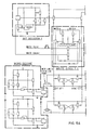
- a cell is selected by simultaneously raising the voltage on the pair of bit lines and lowering the voltage on the word and drain lines it is connected to.
- the method of lowering the voltage on the word and drain lines has almost exclusively been used to cause a higher current to flow through the memory cell and reinforce the state it is in. This method allows a faster read operation because the increased current flow is easier to sense.
- an increase in cell current is highly ditrimental to the ability to change the cells state when writing it
- the current through the modified CTS cell is exponentially related to the voltage from word line to drain line.
- the use of a word to drain line shunt in this case is a simple PN diode, to fix the word to drain line difference is a tremendous aid in stabilizing the cell current even though the word and drain line voltage changes substantially during selection.
- a cell is selected in the word dimension by lowering the voltage on the word and drain line (WL and DL) it is connected to.
- a cell is selected in the bit dimension by raising the voltage on the bit lines (BL and BR) it is connected to.
- a cell that is connected to a selected pair of bit lines and selected word/drain lines is fully selected, and its content may be read or altered. Reading the content of a cell is accomplished by sensing a differential voltage or current in the bit lines.
- the cell contains a "0", which could be defined by transistor NPNL conducting, it could be read by the bit decode circuit raising the voltage of node BIT, and the word decode lowering the voltage of node DL If NPNL was conducting then in fully selected state collector current would flow thru RBL and DL, the base current for NPNL is supplied thru RBR and DR. Transistor PNPL is slightly conducting while PNPR and NPNR are nonconducting. The differential current that flows in the bit lines is determined by the beta of the NPN transistor in the cell. Typically the beta value is 100 and the voltage difference between the bit lines or the differential current between TBSL and TBSR can easily be sensed.
- the bit decode When the bit decode selects the proper bit column to read, it also does one other thing; it enables the write circuit If a pulse occurs on the WC line, which is connected to all write circuits, new data will be written into the selected cell.
- the W1 and WO lines are always out of phase with each other, for the case of writing a "1" the W1 line would be high and WO low.
- the cell is brought into the fully selected state by the word and bit decoders.
- the write circuit is enabled by raising the BS line. The writing is accomplished by a pulse on the WC line. When WC goes high current will flow thru RL and TCL because W1 is high and WO is low. RL and RR regulate the amount of current thru TCL or TCR.
- the state change of the cell corresponds to an impedance change seen on the bit line by TBL Because BL is now in a high impedance state there is no good discharge path for node L. If this condition were to remain then the contents of the next selected cell in that bit column could be altered. To remedy that condition diodes D1 and D2 are connected from node L to the opposite bit line that was raised. At the time that BL changed from supplying the collector current of NPNL to supplying the base cutent of NPNR, BR changed from suppling base current of NPNL to collector current of NPNR. As the current in BR increases its voltage drops to the point where D1 and D2 conduct and discharge node L.
- NPNR base and collector currents of NPNR are eventually supplied by transistors TBSL and TBSR respectively as the write circuit shuts itself off.
- This self limiting feature of the write circuit makes possible high speed write operation and very low power dissipation. It can be appreciated that the write circuit uses power only when the write pulse is high, typically a low duty cycle. At all other times and for all unselected bit columns the write circuit dissipates zero power.
Landscapes
- Engineering & Computer Science (AREA)
- Microelectronics & Electronic Packaging (AREA)
- Computer Hardware Design (AREA)
- Static Random-Access Memory (AREA)
- Semiconductor Memories (AREA)
Applications Claiming Priority (2)
| Application Number | Priority Date | Filing Date | Title |
|---|---|---|---|
| US682391 | 1984-12-17 | ||
| US06/682,391 US4635228A (en) | 1984-12-17 | 1984-12-17 | Random access memory employing unclamped complementary transistor switch (CTS) memory cells and utilizing word to drain line diode shunts |
Publications (2)
| Publication Number | Publication Date |
|---|---|
| EP0185978A2 true EP0185978A2 (fr) | 1986-07-02 |
| EP0185978A3 EP0185978A3 (fr) | 1989-02-08 |
Family
ID=24739499
Family Applications (1)
| Application Number | Title | Priority Date | Filing Date |
|---|---|---|---|
| EP85115320A Ceased EP0185978A3 (fr) | 1984-12-17 | 1985-12-03 | Mémoire écriture-lecture à accès aléatoire |
Country Status (3)
| Country | Link |
|---|---|
| US (1) | US4635228A (fr) |
| EP (1) | EP0185978A3 (fr) |
| JP (1) | JPS61144792A (fr) |
Families Citing this family (1)
| Publication number | Priority date | Publication date | Assignee | Title |
|---|---|---|---|---|
| US4922455A (en) * | 1987-09-08 | 1990-05-01 | International Business Machines Corporation | Memory cell with active device for saturation capacitance discharge prior to writing |
Family Cites Families (7)
| Publication number | Priority date | Publication date | Assignee | Title |
|---|---|---|---|---|
| US3979612A (en) * | 1973-11-21 | 1976-09-07 | Raytheon Company | V-groove isolated integrated circuit memory with integral pinched resistors |
| DE2457921C2 (de) * | 1974-12-07 | 1976-12-09 | Ibm Deutschland | Verfahren und schaltungsanordnung zur erhoehung der schreibgeschwindigkeit in integrierten datenspeichern |
| FR2304991A1 (fr) * | 1975-03-15 | 1976-10-15 | Ibm | Agencement de circuits pour memoire semi-conductrice et son procede de fonctionnement |
| EP0006753B1 (fr) * | 1978-06-30 | 1983-02-16 | Fujitsu Limited | Circuit intégré à semi-conducteur |
| US4168539A (en) * | 1978-09-15 | 1979-09-18 | Gte Laboratories Incorporated | Memory system with row clamping arrangement |
| US4292675A (en) * | 1979-07-30 | 1981-09-29 | International Business Machines Corp. | Five device merged transistor RAM cell |
| US4460984A (en) * | 1981-12-30 | 1984-07-17 | International Business Machines Corporation | Memory array with switchable upper and lower word lines |
-
1984
- 1984-12-17 US US06/682,391 patent/US4635228A/en not_active Expired - Fee Related
-
1985
- 1985-09-12 JP JP60200727A patent/JPS61144792A/ja active Granted
- 1985-12-03 EP EP85115320A patent/EP0185978A3/fr not_active Ceased
Also Published As
| Publication number | Publication date |
|---|---|
| US4635228A (en) | 1987-01-06 |
| JPS61144792A (ja) | 1986-07-02 |
| JPH0259558B2 (fr) | 1990-12-12 |
| EP0185978A3 (fr) | 1989-02-08 |
Similar Documents
| Publication | Publication Date | Title |
|---|---|---|
| US4078261A (en) | Sense/write circuits for bipolar random access memory | |
| US4817051A (en) | Expandable multi-port random access memory | |
| EP0461430B1 (fr) | Circuit de rétablissement pour lignées binaires individuelles | |
| GB1536013A (en) | Data storage memories | |
| EP0019988B1 (fr) | Système de sélection des lignes de mot dans une mémoire bipolaire à accès aléatoire | |
| US3530443A (en) | Mos gated resistor memory cell | |
| EP0183885A1 (fr) | Mémoire à cellules conventionnelles fonctionnant en RAM ou en mémoire associative | |
| EP0222154B1 (fr) | Dispositif et réseau de mémoire semi-conductrice | |
| US4295210A (en) | Power supply system for monolithic cells | |
| EP0284665B1 (fr) | Mémoire statique à semi-conducteurs | |
| EP0185978A2 (fr) | Mémoire écriture-lecture à accès aléatoire | |
| US4292675A (en) | Five device merged transistor RAM cell | |
| US4910711A (en) | Bicmos read/write control and sensing circuit | |
| EP0185156B1 (fr) | Mémoire écriture-lecture à accès aléatoire | |
| US4627034A (en) | Memory cell power scavenging apparatus and method | |
| EP0121423B1 (fr) | Décharge de ligne de mot dans des mémoires semi-conductrices statiques | |
| US4393473A (en) | Random access memory preset circuitry | |
| US4398268A (en) | Semiconductor integrated circuit device | |
| GB2047497A (en) | I2l sensing circuit with increased sensitivity | |
| US4964081A (en) | Read-while-write ram cell | |
| US5251173A (en) | High-speed, low DC power, PNP-loaded word line decorder/driver circuit | |
| US5173877A (en) | BICMOS combined bit line load and write gate for a memory | |
| EP0354950B1 (fr) | Memoire vive bipolaire a courant d'ecriture variable avec l'etat | |
| JPS6010392B2 (ja) | 2ポ−ト・ランダム・アクセス・メモリ素子 | |
| EP0037734B1 (fr) | Circuit intégré de mémoire à semi-conducteurset dispositif de mémoire utilisant ces circuits |
Legal Events
| Date | Code | Title | Description |
|---|---|---|---|
| PUAI | Public reference made under article 153(3) epc to a published international application that has entered the european phase |
Free format text: ORIGINAL CODE: 0009012 |
|
| AK | Designated contracting states |
Kind code of ref document: A2 Designated state(s): DE FR GB |
|
| 17P | Request for examination filed |
Effective date: 19861029 |
|
| PUAL | Search report despatched |
Free format text: ORIGINAL CODE: 0009013 |
|
| AK | Designated contracting states |
Kind code of ref document: A3 Designated state(s): DE FR GB |
|
| 17Q | First examination report despatched |
Effective date: 19900531 |
|
| STAA | Information on the status of an ep patent application or granted ep patent |
Free format text: STATUS: THE APPLICATION HAS BEEN REFUSED |
|
| 18R | Application refused |
Effective date: 19910721 |
|
| RIN1 | Information on inventor provided before grant (corrected) |
Inventor name: MOSLEY, JOSEPH M. Inventor name: JORDY, GEORGE JOHN |