EP0185995B1 - Interrupteur semi-conducteur programmable pour un tableau indicateur influençant la luminosité et procédé pour fabriquer celui-ci - Google Patents
Interrupteur semi-conducteur programmable pour un tableau indicateur influençant la luminosité et procédé pour fabriquer celui-ci Download PDFInfo
- Publication number
- EP0185995B1 EP0185995B1 EP85115442A EP85115442A EP0185995B1 EP 0185995 B1 EP0185995 B1 EP 0185995B1 EP 85115442 A EP85115442 A EP 85115442A EP 85115442 A EP85115442 A EP 85115442A EP 0185995 B1 EP0185995 B1 EP 0185995B1
- Authority
- EP
- European Patent Office
- Prior art keywords
- layer
- pixel
- substrate
- threshold
- electrode
- Prior art date
- Legal status (The legal status is an assumption and is not a legal conclusion. Google has not performed a legal analysis and makes no representation as to the accuracy of the status listed.)
- Expired - Lifetime
Links
Images


Classifications
-
- G—PHYSICS
- G02—OPTICS
- G02F—OPTICAL DEVICES OR ARRANGEMENTS FOR THE CONTROL OF LIGHT BY MODIFICATION OF THE OPTICAL PROPERTIES OF THE MEDIA OF THE ELEMENTS INVOLVED THEREIN; NON-LINEAR OPTICS; FREQUENCY-CHANGING OF LIGHT; OPTICAL LOGIC ELEMENTS; OPTICAL ANALOGUE/DIGITAL CONVERTERS
- G02F1/00—Devices or arrangements for the control of the intensity, colour, phase, polarisation or direction of light arriving from an independent light source, e.g. switching, gating or modulating; Non-linear optics
- G02F1/01—Devices or arrangements for the control of the intensity, colour, phase, polarisation or direction of light arriving from an independent light source, e.g. switching, gating or modulating; Non-linear optics for the control of the intensity, phase, polarisation or colour
- G02F1/13—Devices or arrangements for the control of the intensity, colour, phase, polarisation or direction of light arriving from an independent light source, e.g. switching, gating or modulating; Non-linear optics for the control of the intensity, phase, polarisation or colour based on liquid crystals, e.g. single liquid crystal display cells
- G02F1/133—Constructional arrangements; Operation of liquid crystal cells; Circuit arrangements
- G02F1/135—Liquid crystal cells structurally associated with a photoconducting or a ferro-electric layer, the properties of which can be optically or electrically varied
- G02F1/1354—Liquid crystal cells structurally associated with a photoconducting or a ferro-electric layer, the properties of which can be optically or electrically varied having a particular photoconducting structure or material
-
- G—PHYSICS
- G02—OPTICS
- G02F—OPTICAL DEVICES OR ARRANGEMENTS FOR THE CONTROL OF LIGHT BY MODIFICATION OF THE OPTICAL PROPERTIES OF THE MEDIA OF THE ELEMENTS INVOLVED THEREIN; NON-LINEAR OPTICS; FREQUENCY-CHANGING OF LIGHT; OPTICAL LOGIC ELEMENTS; OPTICAL ANALOGUE/DIGITAL CONVERTERS
- G02F1/00—Devices or arrangements for the control of the intensity, colour, phase, polarisation or direction of light arriving from an independent light source, e.g. switching, gating or modulating; Non-linear optics
- G02F1/01—Devices or arrangements for the control of the intensity, colour, phase, polarisation or direction of light arriving from an independent light source, e.g. switching, gating or modulating; Non-linear optics for the control of the intensity, phase, polarisation or colour
- G02F1/13—Devices or arrangements for the control of the intensity, colour, phase, polarisation or direction of light arriving from an independent light source, e.g. switching, gating or modulating; Non-linear optics for the control of the intensity, phase, polarisation or colour based on liquid crystals, e.g. single liquid crystal display cells
- G02F1/133—Constructional arrangements; Operation of liquid crystal cells; Circuit arrangements
- G02F1/136—Liquid crystal cells structurally associated with a semi-conducting layer or substrate, e.g. cells forming part of an integrated circuit
- G02F1/1362—Active matrix addressed cells
- G02F1/1365—Active matrix addressed cells in which the switching element is a two-electrode device
-
- H—ELECTRICITY
- H10—SEMICONDUCTOR DEVICES; ELECTRIC SOLID-STATE DEVICES NOT OTHERWISE PROVIDED FOR
- H10D—INORGANIC ELECTRIC SEMICONDUCTOR DEVICES
- H10D1/00—Resistors, capacitors or inductors
- H10D1/40—Resistors
-
- H—ELECTRICITY
- H10—SEMICONDUCTOR DEVICES; ELECTRIC SOLID-STATE DEVICES NOT OTHERWISE PROVIDED FOR
- H10W—GENERIC PACKAGES, INTERCONNECTIONS, CONNECTORS OR OTHER CONSTRUCTIONAL DETAILS OF DEVICES COVERED BY CLASS H10
- H10W20/00—Interconnections in chips, wafers or substrates
- H10W20/40—Interconnections external to wafers or substrates, e.g. back-end-of-line [BEOL] metallisations or vias connecting to gate electrodes
- H10W20/49—Adaptable interconnections, e.g. fuses or antifuses
Definitions
- the invention relates to a pixel of a display comprising an insulative transparent substrate, a pixel electrode formed on said substrate and a multilayer threshold element between said pixel electrode and an address line which threshold element comprises layers of substantially amorphous semi-conductor material.
- Such pixel employing a p-i-p structure is described in EP-A-0 126 914.
- semi-conductor layers comprise n-doped sheets and p-doped sheets which are directly or indirectly contacting.
- pixels can be used for forming a matrix array to be used for visual display devices.
- the pixels may consist of liquid crystal elements in which a film or cell of liquid crystal material is positioned between a pair of electrodes.
- Conventional nematic type liquid crystals consist of elongate molecules whose longitudinal axis can be rotated when an electric field of prescribed magnitude is applied to the material. The molecular rotation rotates the polarization of light transmitted through the liquid crystal material.
- liquid crystal display employs twisted nematic crystals sandwiched between a pair of parallel glass sheets and a pair of polarizers respectively on opposite sides of the glass sheets.
- the polarizer on the input side of the display allows ambient light polarized in only one direction to pass into the display.
- the glass sheets have parallel lines formed by etching or the like on the opposing faces thereof.
- the molecules of the nematic crystal material near the surface of each glass plate tend to align their long axes parallel to the lines on the glass plates.
- the plates are oriented relative to each other such that the two sets of lines are nonparallel, e.g. 90 degrees off axis, thus giving the nematic crystals a helical or twisted orientation.
- Polarized light passing through the cell is rotated by the crystals.
- the second polarizer can thus allow the passage of the rotated light out of the cell.
- Application of an electric field across the cell rotates or "untwists" the molecules so that their axes extend substantially parallel to each other, thus blocking passage of light through the cell and the polarizers.
- the pixels are arranged into M rows and N columns defining a matrix array that is addressed using conventional "X-Y" addressing techniques which employ M + N address lines.
- Each pixel possesses a unique X-Y location in the matrix which may be addressed by a corresponding combination of X and Y addressing lines.
- a threshold device must be incorporated into each liquid crystal picture element.
- Thin film field-effect transistors have also been used as isolation devices in liquid crystal pixel elements. Transistors have a more complex structure than do diodes however and are three terminal devices which complicate pixel manufacture.
- optical radiation can be used for programming a threshold voltage at which said threshold element conducts current between the address line and the pixel electrode.
- the threshold of each threshold element can be set by directing radiation through the substrate and into each threshold device.
- the present invention also provides for a bidirectional threshold element formed of deposited semiconductor materials having a selected thickness as well as a selected area.
- the selected area is on the order of 900 ⁇ m2.
- Opaque metal conductors formed at each end of the device optically insulate the device from spurious incident light.
- the threshold device can be incorporated into a subassembly for a light influencing display.
- an improvement for a subassembly usable in a light influencing display includes first and second bidirectional threshold elements coupled between a display electrode and an adjacent address line.
- the threshold elements can be series or parallel coupled to provide a bidirectional, symmetrical threshold device.
- the bidirectional threshold element can be formed of multiple layers of semiconductor material.
- a subassembly usable in a light influencing display includes a substrate, an electrode formed thereon, an adjacent address line and a bidirectional, deposited semiconductor means for forming a threshold coupled between the electrode and the address line.
- the threshold means can include first and second threshold elements that may be parallel or series coupled. In an alternate embodiment of the invention, one of the threshold elements can be formed partly overlying the address line.
- Figure 1 illustrates a top planar view of a portion of a subassembly 10 usable in a light influencing display in accordance with the present invention.
- the subassembly 10 includes a substrate 15 which may be glass or some other substantially transparent insulator. Formed on the substrate 15 are a plurality of spaced apart electrodes 20 through 30. Each of the electrodes 20 through 30 forms a portion of a pixel in an assembled light influencing display.
- the electrodes 20 through 30 are formed of a transparent conductor such as indium tin oxide.
- Each of the electrodes 20 through 24 is coupled to an address bus 32 by a respective connector element 34 through 38.
- a second address bus 42 spaced apart from the first address bus 32, essentially parallel thereto, is also formed on the substrate 15.
- Each of the electrodes 26 through 30 is coupled to the address line 42 by a connector element 44 through 48.
- FIG 2 is an enlarged sectional view incorporating the subassembly 10 and taken along the line 2-2 of Figure 1.
- the subassembly 10 has been combined with the spaced apart substrate 50 upon which is formed a second indium tin oxide electrode 52.
- the spaced apart electrodes 24 and 52 form the control electrodes for a pixel of a light influencing display.
- a region 54 between the electrodes 24 and 52 is filled with a light influencing material 56.
- light influencing material is meant any material which emits light or can be used to selectively vary the intensity, phase, or polarization of light either being reflected from or transmitted through the material. Liquid crystal material is only one such material having these characteristics.
- the light influencing material 56 can be of any conventional variety, as for example, nematic liquid crystal display material.
- each light influencing pixel element a nonlinear threshold element for purposes of increasing the number of possible lines in the display.
- a nonlinear threshold element is a two terminal bidirectional n-i-n or n+in+ threshold element having three layers formable from deposited amorphous semiconductor alloy as discussed further herein.
- the electrodes 24 and 52, as well as the underlying substrates 15 and 50, are treated as is conventional to align the molecules of the display material 56.
- This treatment can include, for example, applying an alignment coating over the electrodes 24 and 52.
- the fragmentary sectional view of the subassembly 10 of Figure 2 includes an n-i-n threshold element 60.
- a pad 62 of deposited chromium partly overlies the electrode 24 between the electrode 24 and the element 60 and forms a pixel electrode.
- the threshold element 60 is formed between the metal pad 62, such as chromium, and a second deposited metal layer 64, such as chromium or an alloy of molybdenum and tantalum.
- the metal pad 62 interconnects the pixel electrode 24 with a lower n-doped layer 66 of the threshold device 60.
- An intrinsic layer 68 is positioned between the n-doped layer 66 and an upper n-doped layer 70.
- the top metal layer 64 is deposited to a thickness on the order of 100 nm.
- the upper metal layer 64 is thick enough so as to be opaque to incident visible light.
- the metal layer 64 blocks and isolates the n-i-n threshold element 60 from any incident light or radiation which might pass through the substrate 50 and also functions as a highly conductive region or part of the address line 32.
- the pad 62 is formed so as to be partly transmissive to light.
- the portion of the n-i-n threshold device 60 vertically disposed between the metal pad 62 and the metal layer 64 is operative to provide the requisite threshold for the electrode 24.
- the address line 32 is formed as a continuous multilayer structure including the deposited amorphous semiconductor alloy layers 66 through 70 along with the overlying top metal layer 64.
- the threshold of the element 60 can be adjusted to a predetermined value by incident radiation such as visible light.
- incident radiation such as visible light.
- radiation from a selected source can be directed against the transparent substrate 15.
- the radiation passes through the substrate 15 and also through the chromium layer or pad 62.
- the chromium pad 62 in this embodiment is deposited to a thickness on the order of 5 to 10 nm so as to be 10% transmissive.
- the radiation can be visible light, preferably red light with a wavelength on the order of 600 nm for more effective penetration of, the threshold element 60.
- a polarizer 74 is applied to an outer surface 76 of the substrate 15.
- a mirror 78 is applied over the polarizer 74 completing the subassemby 10.
- the subassembly 10 can then be combined with the second substrate 50 carrying the electrode 52 and light influencing material 56 to form a completed display pixel.
- Figure 4 illustrates a step of a method for manufacturing a pixel according to the present invention.
- a layer of indium tin oxide is first deposited on the substrate 15.
- a layer of chromium is deposited.
- electrodes such as the electrode 24, with an overlying pad or layer 80 of chromium.
- the metal layer 80 in combination with the electrode 24 form a two-layer conductor having a selected size and shape.
- the thickness of the chromium layer can be on the order of 5 to 10 nm so that it is approximately 10% transmissive.
- a continuous layer 82 of n-type semiconductor material is deposited over the substrate 15, and the chromium pads such as the pad or layer 80.
- the layer 82 is deposited with n-type doping.
- a layer of intrinsic semiconductor material 84 is then deposited overlying the n-type layer 82.
- a second n-type layer 86 of semiconductor material is deposited overlying the intrinsic layer 84.
- the layers 82 through 88 form a multilayer structure 90 which can be processed further.
- the layers 82 through 86 are preferably formed from deposited semiconductor material.
- the deposited semiconductor material is preferably an amorphous semiconductor alloy including silicon.
- the amorphous silicon alloy can also include hydrogen and/or fluorine and can be formed by, for example, plasma-assisted chemical vapor deposition, i.e. glow discharge as disclosed, for example, in US-A-4,226,898.
- amorphous is meant an alloy or material which has long-range disorder, although it may have short-or intermediate-range order or even contain at times some crystalline inclusions.
- the layers 82 through 86 can be deposited in a continuously maintained partial vacuum.
- the glow discharge decomposition of at least silane gas (SiH4) and/or silicon tetrafluoride (SiF4) gas may be used to deposit the layers 82 through 86.
- the metal layer 88 may be deposited using any known conventional deposition method such as standard methods of vacuum deposition.
- the multilayer structure 90 is patterned using photolithography and a mask to form the address lines 32 and 42 as well as the respective threshold elements such as the element 60.
- a plasma etch may be used to etch away the unwanted portions of the multilayer structure 90.
- the metal layer 88 which is patterned to form the upper layer 64 of the address line such as 32 protects the underlying n-i-n layers from being etched away.
- the metal layer 80 is etched away forming the pad 62 and exposing the electrode 24 as illustrated in Figure 2.
- the threshold elements, for example element 60, of the subassembly 10 can then be optically programmed.
- the method as illustrated by the steps of Figures 4, 5, 6 and the sectional views of Figures 2 and 3 has only two steps of patterning and etching. This is due to the fact that the n-i-n layers 66-70 extend continuously between the electrodes, such as the electrodes 22 and 24, as best shown in Figure 2.
- the subassembly 10 formed by the present method thus has continuously extending multilayer address lines, such as the lines 32 and 42.
- the present method is simple and has fewer steps than would be the case if discrete threshold devices were formed.
- FIG. 7 A further embodiment of the invention is illustrated in Figure 7.
- a subassembly 98 for a light influencing display is formed with a glass substrate 100.
- the substrate 100 has formed thereon a pixel electrode 102.
- the pixel electrode 102 is formed, of a transparent conductive material such as indium tin oxide.
- Formed on a portion of the electrode 102 is a layer 104 of chromium.
- a layer of n-type semiconductor material 106 Overlying the layer 104 of chromium is a layer of n-type semiconductor material 106.
- the n-doped layer 106 is restricted to overlie the chromium layer 104.
- a layer 108 of intrinsic semiconductor material overlies the n-type layer 106 and a portion of the substrate 100.
- a second n-type semiconductor layer 110 overlies the intrinsic semiconductor layer 108.
- a metal layer 112 of chromium or a molybdenum-tantalum alloy overlies the doped semiconductor layer 110.
- the layer 112 can function as an address line analogous to the layer 64 of Figure 2.
- the n-i-n isolation device, formed of layers 106 through 110 is vertically arrayed with respect to the substrate 100 and is electrically coupled between the chromium layer 104 and the address line 112.
- the layers of semiconductor material 106, 108 and 110 of the subassembly 98 can be formed of amorphous semiconductor alloys of the type previously disclosed herein.
- the embodiment of Figure 7 has the further advantage that by limiting the area of the n-type layer 106, leakage current due to edge effects is reduced.
- Figure 8 illustrates part of a method of making the subassembly 98 of Figure 7.
- a layer of indium tin oxide is first applied over an upper surface of the substrate 100.
- a layer of chromium is then formed by vacuum deposition of a conventional variety overlying the layer of indium tin oxide.
- a first layer of n-type semiconductor material is then deposited overlying the layer of chromium.
- the layers of indium tin oxide, chromium and n-type semiconductor material are patterned so as to form a multilayer structure 114, as illustrated in Figure 8.
- the structure 114 has a bottom layer formed of the shaped indium tin oxide electrode 102, a chromium layer 116 overlying the indium tin oxide layer and an n-type semiconductor layer 118 overlying the chromium layer 116.
- the layers 102 and 116 form a multilayer conductor having an adjacent overlying layer 118 of semiconductor material.
- a continuous layer 120 of intrinsic semiconductor material is then deposited over the doped semiconductor layer 118 and the exposed regions of the substrate 100.
- a second n-type doped semiconductor layer 122 is then deposited overlying the intrinsic layer 120.
- a continuous metal layer 124 is deposited overlying the second doped semiconductor layer 120.
- the layers 120 and 122 may be deposited using the glow discharge deposition technique in a continuously maintained partial vacuum as previously discussed.
- the layers 120, 122 and 124 are etched using a layer of protective photoresist so as to form the layers 108 through 112 of Figure 7.
- the n+ type semiconductor layer 118 and the chromium layer 116 of Figure 8 are etched so as to form the layers 106 and 104 respectively of Figure 7.
- n-i-n devices of the present invention demonstrate nonsymmetries with respect to their threshold characteristics. These nonsymmetries are believed to be in part created or caused by the fabrication process. From the point of view of incorporating such n-i-n devices as bidirectional threshold elements for use with liquid crystal display pixels these nonsymmetries may present a problem.
- the basis of the problem lies in the fact that the nonsymmetrical characteristic results in an average DC signal being applied to the liquid crystal display, in a given direction, over a period of time. It is known that such DC potentials applied to liquid crystal display pixels will result in degradation of the liquid crystal display material. Hence, such DC potentials are to be avoided if at all possible. Additionally, the nonsymmetries complicate the design of the addressing circuitry and are undesirable for that reason also.
- a subassembly 130 for a light influencing display pixel is illustrated which overcomes the asymmetries found in individual n-i-n devices.
- the subassembly 130 is formed on a glass substrate 132 and includes an address bus 134 which is formed adjacent to a transparent conducting pixel electrode 136.
- the electrode 136 is treated in a conventional manner so as to provide for the proper alignment of the liquid display material.
- the electrode 136 includes a cut-out region 137.
- the cut-out region 137 could be eliminated without departing from the spirit and scope of the present invention.
- the cut-out region 137 provides an advantage in the overall structure of the subassembly 130.
- a rectangular metal pad 138 is formed overlying the cut-out region 137 of the electrode 136.
- the pad 138 can be formed, for example, of vacuum deposited chromium. As can be seen from Figure 9, ends of the pad 138 overlap the electrode 136.
- a multilayer structure 140 interconnects the address bus 134 with the metal pad 138.
- the multilayer structure 140 includes two series coupled n-i-n devices. The n-i-n devices are series coupled in reverse fashion such that the asymmetrical characteristics are additive in reverse order and cancel each other out. This results in a symmetrical, bilateral, nonlinear characteristic between the address line 134 and the metal pad 138.
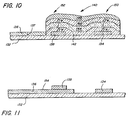
- Figure 10 is a sectional view taken along line 10-10 of Figure 9 and illustrates the structure of the element 140.
- the address lead 134 is shown in section positioned on the substrate 132. Spaced over from the address lead 134 is a portion of the metal pad 138 also formed on the substrate 132. Overlying the address line 134 and the metal pad 138 is the multilayer structure 140.
- the structure 140 includes a first layer of doped semiconductor material 142.
- the layer 142 is doped with n-type doping.
- Overlying the layer 142 is a layer of deposited intrinsic semiconductor material 144.
- Overlying the layer 144 is a second doped layer of semiconductor material 146.
- the layer 146 is doped with n-type doping.
- Overlying the second doped layer of semiconductor material 146 is a deposited layer of metal 148.
- the layer of metal 148 may be vacuum deposited and may be formed of chromium or an alloy of molybdenum-tantalum.
- a first n-i-n device 150 is formed in the element 140 vertically arrayed with respect to the address bus 134 and coupled between the address bus 134 and the metal layer 148.
- a second n-i-n device 152 is formed vertically arrayed above the metal pad 138 coupled between the metal pad 138 and the metal layer 148. The two n-i-n devices 150 and 152 are series coupled by the metal layer 148.
- n-i-n devices 150 and 152 could be formed in parallel coupled between the address line 134 and the electrode 136. Formation of the device 152 over the cut-out 137 results in a well defined operative cross section thereto.
- Figure 11 is a sectional view taken along line 11-11 of Figure 9 and illustrates further the relationship between the metal address bus 134 and the spaced apart metal pad 138.
- the metal pad 138 positioned in part on an upper surface 154 of the indium tin oxide electrode 136 whereas the address bus 134 is positioned on the substrate 132.
Landscapes
- Physics & Mathematics (AREA)
- Nonlinear Science (AREA)
- Mathematical Physics (AREA)
- Chemical & Material Sciences (AREA)
- Crystallography & Structural Chemistry (AREA)
- General Physics & Mathematics (AREA)
- Optics & Photonics (AREA)
- Engineering & Computer Science (AREA)
- Microelectronics & Electronic Packaging (AREA)
- Liquid Crystal (AREA)
- Thin Film Transistor (AREA)
- Devices For Indicating Variable Information By Combining Individual Elements (AREA)
Claims (8)
- Pixel d'un écran comprenant un substrat transparent isolant (15, 100, 132), une électrode de pixel (24, 62, 80, 102, 136) formée sur ledit substrat (15, 100, 132), un élément de seuil multicouche (60, 98, 140, 150) placé entre ladite électrode de pixel (24, 62, 80, 102, 136) et une ligne d'adresse (32, 134) lequel élément de seuil comporte des couches (66, 68, 70) en matériau semi-conducteur sensiblement amorphe, caractérisé en ce que ledit élément de seuil(60, 98, 140, 150) a un seuil qui est réglable par irradiation au moyen d'un rayonnement sélectionné et qui est formé d'un élément nin ou d'un élément n+in+ comprenant une première couche amorphe dopée n (66, 82, 106, 118, 142), une couche intrinsèque (i) (68, 84, 120, 144) recouvrant ladite première couche dopée n (66, 82, 106, 118, 142), et une seconde couche amorphe dopée n (70, 86, 110, 122, 146) recouvrant ladite couche intrinsèque (68, 84, 108, 120, 144), ladite électrode de pixel (24, 62, 80, 102, 136) étant au moins en partie transparente audit rayonnement sélectionné.
- Pixel selon la revendication 1, caractérisé en ce que ladite seconde couche dopée n (70, 86, 110, 122, 146) est au moins en partie recouverte d'une couche métallique (64) qui est suffisamment épaisse pour être opaque à la lumière visible incidente et pour fonctionner comme région fortement conductrice et/ou comme partie de ladite ligne d'adresse (32).
- Pixel selon la revendication 2, caractérisé en ce que ledit bloc (62, 80, 104, 116, 138) a un coefficient de transmission de la lumière visible d'environ 10 %.
- Pixel selon l'une des revendications précédentes, caractérisé en ce que ledit substrat (15) est sensiblement transparent au rayonnement incident et en ce qu'un polariseur (74) est appliqué sur la surface extérieure (76) dudit substrat (15).
- Pixel selon la revendication 4, caractérisé en ce qu'un miroir (78) est appliqué sur ledit polariseur (74).
- Pixel selon l'une quelconque des revendications précédentes, caractérisé en ce que deux éléments nin (150) ou éléments n+in+ sont disposés sur ledit substrat (132) et couplés en série entre ladite électrode de pixel (136) et ladite ligne d'adresse (134) par une couche métallique (148).
- Pixel selon l'une des revendications précédentes, caractérisé en ce que ledit matériau semi-conducteur amorphe comprend du silicium et de l'hydrogène et du fluor en option.
- Pixel selon l'une des revendications précédentes, caractérisé en ce que ledit élément de seuil est placé entre ledit substrat (15, 132) et ladite électrode de pixel (24, 62, 136) d'une part et d'autre part un matériau influençant la lumière (56), une seconde électrode (52) et un second substrat (50).
Applications Claiming Priority (2)
| Application Number | Priority Date | Filing Date | Title |
|---|---|---|---|
| US06/679,770 US4698627A (en) | 1984-04-25 | 1984-12-10 | Programmable semiconductor switch for a light influencing display and method for making same |
| US679770 | 1991-04-03 |
Publications (3)
| Publication Number | Publication Date |
|---|---|
| EP0185995A2 EP0185995A2 (fr) | 1986-07-02 |
| EP0185995A3 EP0185995A3 (en) | 1986-10-01 |
| EP0185995B1 true EP0185995B1 (fr) | 1992-03-04 |
Family
ID=24728295
Family Applications (1)
| Application Number | Title | Priority Date | Filing Date |
|---|---|---|---|
| EP85115442A Expired - Lifetime EP0185995B1 (fr) | 1984-12-10 | 1985-12-05 | Interrupteur semi-conducteur programmable pour un tableau indicateur influençant la luminosité et procédé pour fabriquer celui-ci |
Country Status (4)
| Country | Link |
|---|---|
| US (1) | US4698627A (fr) |
| EP (1) | EP0185995B1 (fr) |
| JP (1) | JPS61153692A (fr) |
| DE (1) | DE3585509D1 (fr) |
Families Citing this family (13)
| Publication number | Priority date | Publication date | Assignee | Title |
|---|---|---|---|---|
| US4758896A (en) * | 1985-12-10 | 1988-07-19 | Citizen Watch Co., Ltd. | 3-Dimensional integrated circuit for liquid crystal display TV receiver |
| US4728802A (en) * | 1986-01-21 | 1988-03-01 | Ovonic Imaging Systems, Inc. | Balanced drive photosensitive pixel and method of operating the same |
| DE3714164A1 (de) * | 1986-04-30 | 1987-11-05 | Sharp Kk | Fluessigkristallanzeige |
| US5008617A (en) * | 1989-06-20 | 1991-04-16 | Energy Conversion Devices, Inc. | Functional testing of ultra large area, ultra large scale integrated circuits |
| JPH0830825B2 (ja) * | 1990-04-20 | 1996-03-27 | シャープ株式会社 | アクティブマトリクス表示装置 |
| EP0521565B1 (fr) * | 1991-07-04 | 1998-01-07 | Koninklijke Philips Electronics N.V. | Dispositif semiconducteur et procédé de fabrication de ce dispositif ainsi que dispositif d'affichage munie d'un tel dispositif semiconducteur |
| GB9115401D0 (en) * | 1991-07-17 | 1991-09-04 | Philips Electronic Associated | Matrix display device and its method of operation |
| GB9115402D0 (en) * | 1991-07-17 | 1991-09-04 | Philips Electronic Associated | Matrix display device and its method of operation |
| DE69326203T2 (de) * | 1992-07-03 | 2000-05-18 | Citizen Watch Co., Ltd. | Flüssigkristall-Anzeigevorrichtung mit nichtlinearen Widerstandselementen |
| GB9222840D0 (en) * | 1992-10-31 | 1992-12-16 | Smiths Industries Plc | Electronic assemblies |
| JP2915724B2 (ja) * | 1992-11-25 | 1999-07-05 | シャープ株式会社 | 表示装置 |
| US6629292B1 (en) * | 2000-10-06 | 2003-09-30 | International Business Machines Corporation | Method for forming graphical images in semiconductor devices |
| JP3980462B2 (ja) * | 2002-10-30 | 2007-09-26 | 株式会社 日立ディスプレイズ | 画像表示装置 |
Family Cites Families (19)
| Publication number | Priority date | Publication date | Assignee | Title |
|---|---|---|---|---|
| FR1493449A (fr) * | 1966-04-25 | 1967-09-01 | Csf | Nouvelle structure à semi-conducteur |
| US3426295A (en) * | 1966-05-16 | 1969-02-04 | Bell Telephone Labor Inc | Negative resistance microwave device |
| FR2319267A1 (fr) * | 1973-07-03 | 1977-02-18 | Radiotechnique Compelec | Dispositif electroluminescent a seuil |
| US4103297A (en) * | 1976-12-20 | 1978-07-25 | Hughes Aircraft Company | Light-insensitive matrix addressed liquid crystal display system |
| US4191454A (en) * | 1977-06-20 | 1980-03-04 | Hughes Aircraft Company | Continuous silicon MOS AC light valve substrate |
| US4233603A (en) * | 1978-11-16 | 1980-11-11 | General Electric Company | Multiplexed varistor-controlled liquid crystal display |
| US4239346A (en) * | 1979-05-23 | 1980-12-16 | Hughes Aircraft Company | Compact liquid crystal display system |
| CA1121489A (fr) * | 1979-05-30 | 1982-04-06 | Northern Telecom Limited | Afficheurs a cristal liquide controles par dispositif metal-isolant-metal |
| US4251136A (en) * | 1979-07-25 | 1981-02-17 | Northern Telecom Limited | LCDs (Liquid crystal displays) controlled by thin film diode switches |
| US4223308A (en) * | 1979-07-25 | 1980-09-16 | Northern Telecom Limited | LCDs (Liquid crystal displays) controlled by thin film diode switches |
| GB2056739B (en) * | 1979-07-30 | 1984-03-21 | Sharp Kk | Segmented type liquid crystal display and driving method thereof |
| JPS5685792A (en) * | 1979-12-14 | 1981-07-13 | Citizen Watch Co Ltd | Liquid crystal display unit |
| FR2505070B1 (fr) * | 1981-01-16 | 1986-04-04 | Suwa Seikosha Kk | Dispositif non lineaire pour un panneau d'affichage a cristaux liquides et procede de fabrication d'un tel panneau d'affichage |
| FI61983C (fi) * | 1981-02-23 | 1982-10-11 | Lohja Ab Oy | Tunnfilm-elektroluminensstruktur |
| US4403217A (en) * | 1981-06-18 | 1983-09-06 | General Electric Company | Multiplexed varistor-controlled liquid crystal display |
| FR2512240A1 (fr) * | 1981-08-25 | 1983-03-04 | Thomson Csf | Dispositif de visualisation a commande electrique utilisant un element non lineaire en couche epaisse et son procede de fabrication |
| FR2512239A1 (fr) * | 1981-08-25 | 1983-03-04 | Thomson Csf | Dispositif de visualisation a commande electrique |
| JPS59158553A (ja) * | 1983-02-28 | 1984-09-08 | Toshiba Corp | 光学的固体装置 |
| EP0126914A2 (fr) * | 1983-04-12 | 1984-12-05 | Granotechnik AG | Unité de contrôle pour un dispositif d'affichage sensible aux champs électriques au moyen d'éléments semi-conducteurs |
-
1984
- 1984-12-10 US US06/679,770 patent/US4698627A/en not_active Expired - Lifetime
-
1985
- 1985-12-05 DE DE8585115442T patent/DE3585509D1/de not_active Expired - Fee Related
- 1985-12-05 EP EP85115442A patent/EP0185995B1/fr not_active Expired - Lifetime
- 1985-12-09 JP JP60276658A patent/JPS61153692A/ja active Pending
Also Published As
| Publication number | Publication date |
|---|---|
| EP0185995A2 (fr) | 1986-07-02 |
| JPS61153692A (ja) | 1986-07-12 |
| US4698627A (en) | 1987-10-06 |
| DE3585509D1 (de) | 1992-04-09 |
| EP0185995A3 (en) | 1986-10-01 |
Similar Documents
| Publication | Publication Date | Title |
|---|---|---|
| EP0654828B1 (fr) | TFT avec capacité parasite réduite | |
| US7211827B2 (en) | Thin film transistor array panel and liquid crystal display including the panel | |
| EP0534467B1 (fr) | Structure d'électrodes d'un dispositif d'affichage à cristal liquide et procédé de fabrication de dispositif d'affichage à cristal liquide | |
| USRE39798E1 (en) | Active matrix LCD device with image signal lines having a multilayered structure | |
| EP0166948B1 (fr) | Dispositifs d'affichage et sous-ensembles avec électrodes pour les éléments d'image | |
| US7102168B2 (en) | Thin film transistor array panel for display and manufacturing method thereof | |
| US7301170B2 (en) | Thin film transistor array panel and method for manufacturing the same | |
| EP0136509B1 (fr) | Dispositif d'affichage actif du type à matrice | |
| KR100675631B1 (ko) | 횡전계방식 액정표시장치 및 그 제조방법 | |
| US7355206B2 (en) | Thin film transistor array panel and manufacturing method thereof | |
| US4704002A (en) | Dot matrix display panel with a thin film transistor and method of manufacturing same | |
| US5193017A (en) | Reflective-type active matrix liquid crystal display device | |
| US5796448A (en) | Structure for a parasitic capacitor and a storage capacitor in a thin film transistor-liquid crystal display and a method for making the same | |
| US5231039A (en) | Method of fabricating a liquid crystal display device | |
| EP0329887B1 (fr) | Dispositif d'affichage à cristaux liquides | |
| US7138655B2 (en) | Thin film transistor array panel including symmetrically aligned thin film transistors and manufacturing method thereof | |
| US4698627A (en) | Programmable semiconductor switch for a light influencing display and method for making same | |
| US20080299712A1 (en) | Manufacturing method of a thin film transistor array panel | |
| US20040056987A1 (en) | Liquid crystal display and thin film transistor array panel therefor | |
| US5953085A (en) | Liquid crystal display device having a storage capacitor | |
| US7605416B2 (en) | Thin film translator array panel and a method for manufacturing the panel | |
| US20060131582A1 (en) | Thin film transistor array panel and manufacturing method thereof | |
| US7045373B2 (en) | Manufacturing method for in-plane switching mode LCD unit with fewer masking process | |
| EP0567684A1 (fr) | Dispositif électro-optique | |
| EP0335724A2 (fr) | Riseau de transistor couche mince pour un dispositif électro-optique et procédé pour sa fabrication |
Legal Events
| Date | Code | Title | Description |
|---|---|---|---|
| PUAI | Public reference made under article 153(3) epc to a published international application that has entered the european phase |
Free format text: ORIGINAL CODE: 0009012 |
|
| AK | Designated contracting states |
Kind code of ref document: A2 Designated state(s): DE FR GB IT NL SE |
|
| PUAL | Search report despatched |
Free format text: ORIGINAL CODE: 0009013 |
|
| AK | Designated contracting states |
Kind code of ref document: A3 Designated state(s): DE FR GB IT NL SE |
|
| 17P | Request for examination filed |
Effective date: 19870224 |
|
| 17Q | First examination report despatched |
Effective date: 19890428 |
|
| GRAA | (expected) grant |
Free format text: ORIGINAL CODE: 0009210 |
|
| AK | Designated contracting states |
Kind code of ref document: B1 Designated state(s): DE FR GB IT NL SE |
|
| ITF | It: translation for a ep patent filed | ||
| REF | Corresponds to: |
Ref document number: 3585509 Country of ref document: DE Date of ref document: 19920409 |
|
| ET | Fr: translation filed | ||
| PG25 | Lapsed in a contracting state [announced via postgrant information from national office to epo] |
Ref country code: GB Effective date: 19921205 |
|
| PG25 | Lapsed in a contracting state [announced via postgrant information from national office to epo] |
Ref country code: SE Effective date: 19921206 |
|
| PLBE | No opposition filed within time limit |
Free format text: ORIGINAL CODE: 0009261 |
|
| STAA | Information on the status of an ep patent application or granted ep patent |
Free format text: STATUS: NO OPPOSITION FILED WITHIN TIME LIMIT |
|
| 26N | No opposition filed | ||
| PG25 | Lapsed in a contracting state [announced via postgrant information from national office to epo] |
Ref country code: NL Effective date: 19930701 |
|
| GBPC | Gb: european patent ceased through non-payment of renewal fee |
Effective date: 19921205 |
|
| NLV4 | Nl: lapsed or anulled due to non-payment of the annual fee | ||
| PG25 | Lapsed in a contracting state [announced via postgrant information from national office to epo] |
Ref country code: FR Effective date: 19930831 |
|
| PG25 | Lapsed in a contracting state [announced via postgrant information from national office to epo] |
Ref country code: DE Effective date: 19930901 |
|
| REG | Reference to a national code |
Ref country code: FR Ref legal event code: ST |
|
| EUG | Se: european patent has lapsed |
Ref document number: 85115442.7 Effective date: 19930709 |