EP0186421A1 - Cellules de mémoire du type ECL - Google Patents
Cellules de mémoire du type ECL Download PDFInfo
- Publication number
- EP0186421A1 EP0186421A1 EP85309202A EP85309202A EP0186421A1 EP 0186421 A1 EP0186421 A1 EP 0186421A1 EP 85309202 A EP85309202 A EP 85309202A EP 85309202 A EP85309202 A EP 85309202A EP 0186421 A1 EP0186421 A1 EP 0186421A1
- Authority
- EP
- European Patent Office
- Prior art keywords
- cell
- polysilicon
- metal
- memory cell
- schottky diode
- Prior art date
- Legal status (The legal status is an assumption and is not a legal conclusion. Google has not performed a legal analysis and makes no representation as to the accuracy of the status listed.)
- Withdrawn
Links
Images


Classifications
-
- H—ELECTRICITY
- H10—SEMICONDUCTOR DEVICES; ELECTRIC SOLID-STATE DEVICES NOT OTHERWISE PROVIDED FOR
- H10B—ELECTRONIC MEMORY DEVICES
- H10B10/00—Static random access memory [SRAM] devices
- H10B10/10—SRAM devices comprising bipolar components
-
- H—ELECTRICITY
- H10—SEMICONDUCTOR DEVICES; ELECTRIC SOLID-STATE DEVICES NOT OTHERWISE PROVIDED FOR
- H10D—INORGANIC ELECTRIC SEMICONDUCTOR DEVICES
- H10D64/00—Electrodes of devices having potential barriers
- H10D64/01—Manufacture or treatment
- H10D64/012—Manufacture or treatment of electrodes comprising a Schottky barrier to a semiconductor
- H10D64/0121—Manufacture or treatment of electrodes comprising a Schottky barrier to a semiconductor to Group IV semiconductors
-
- H—ELECTRICITY
- H10—SEMICONDUCTOR DEVICES; ELECTRIC SOLID-STATE DEVICES NOT OTHERWISE PROVIDED FOR
- H10D—INORGANIC ELECTRIC SEMICONDUCTOR DEVICES
- H10D84/00—Integrated devices formed in or on semiconductor substrates that comprise only semiconducting layers, e.g. on Si wafers or on GaAs-on-Si wafers
- H10D84/01—Manufacture or treatment
- H10D84/0112—Integrating together multiple components covered by H10D8/00, H10D10/00 or H10D18/00, e.g. integrating multiple BJTs
-
- H—ELECTRICITY
- H10—SEMICONDUCTOR DEVICES; ELECTRIC SOLID-STATE DEVICES NOT OTHERWISE PROVIDED FOR
- H10D—INORGANIC ELECTRIC SEMICONDUCTOR DEVICES
- H10D84/00—Integrated devices formed in or on semiconductor substrates that comprise only semiconducting layers, e.g. on Si wafers or on GaAs-on-Si wafers
- H10D84/01—Manufacture or treatment
- H10D84/02—Manufacture or treatment characterised by using material-based technologies
- H10D84/03—Manufacture or treatment characterised by using material-based technologies using Group IV technology, e.g. silicon technology or silicon-carbide [SiC] technology
- H10D84/038—Manufacture or treatment characterised by using material-based technologies using Group IV technology, e.g. silicon technology or silicon-carbide [SiC] technology using silicon technology, e.g. SiGe
-
- Y—GENERAL TAGGING OF NEW TECHNOLOGICAL DEVELOPMENTS; GENERAL TAGGING OF CROSS-SECTIONAL TECHNOLOGIES SPANNING OVER SEVERAL SECTIONS OF THE IPC; TECHNICAL SUBJECTS COVERED BY FORMER USPC CROSS-REFERENCE ART COLLECTIONS [XRACs] AND DIGESTS
- Y10—TECHNICAL SUBJECTS COVERED BY FORMER USPC
- Y10S—TECHNICAL SUBJECTS COVERED BY FORMER USPC CROSS-REFERENCE ART COLLECTIONS [XRACs] AND DIGESTS
- Y10S148/00—Metal treatment
- Y10S148/14—Schottky barrier contacts
-
- Y—GENERAL TAGGING OF NEW TECHNOLOGICAL DEVELOPMENTS; GENERAL TAGGING OF CROSS-SECTIONAL TECHNOLOGIES SPANNING OVER SEVERAL SECTIONS OF THE IPC; TECHNICAL SUBJECTS COVERED BY FORMER USPC CROSS-REFERENCE ART COLLECTIONS [XRACs] AND DIGESTS
- Y10—TECHNICAL SUBJECTS COVERED BY FORMER USPC
- Y10S—TECHNICAL SUBJECTS COVERED BY FORMER USPC CROSS-REFERENCE ART COLLECTIONS [XRACs] AND DIGESTS
- Y10S148/00—Metal treatment
- Y10S148/147—Silicides
Definitions
- ECL Emitter Coupled Logic
- the basic structure of an Emitter Coupled Logic (ECL) bipolar memory cell comprises a pair of memory transistors cross coupled to form a flip-flop circuit.
- the collectors of the memory transistors are respectively connected to the Vcc word line either through a resistive load or through a PNP load.
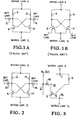
- a diode design or an additional emitter design is used as respectively shown in Figures 1a and 1b representing prior art ECL structures.
- Integrated Injection Logic I 2 L or merged transistor logic has also been used in memory applications wherein the Vcc word line I is coupled to the memory cell through a PNP load having its collector connected to the base of the memory transistor and the base of the PNP load is connected to word line II.
- Typical of such a construction is the bipolar memory cell shown in Fulton U.S. Patent 3,090,807.
- this type of logic has the disadvantage that the cell swings are very small, i.e. about 0.2 volts which creates problems with sensing the state of the cell. This also makes the design more sensitive to noise which can, therefore, make the cell difficult to read.
- Such designs have also tended to be slow due to the saturated nature of
- ECL designs have been quite suitable in the past for cells which are large, i.e., cells used in L.S.I and, in some instances, VLSI structures.
- the space taken by the device was not critical, thus permitting a number of contact areas and isolation tubs.
- CTS Complimentary Transistor Switch
- an ECL bipolar memory cell using Schottky diode connections to bit lines to provide improved resistance to latch-up.
- the cathode of the Schottky diode preferably comprises polysilicon to improve performance of the diode and facilitate construction of the diode and resistor portions of the cell.
- an ECL bipolar memory cell structure having improved resistance to latch-up comprises: a pair of cross-coupled transistors having their respective bases coupled to the collector of the other transistor and their emitters connected together to a word line; a load device comprising a resistor or a PNP load respectively connected between a second word line and each base-collector coupling; and a pair of Schottky diodes respectively connecting left and right bit lines to the base-collector couplings; whereby the low minority carrier injection efficiency of the Schottky diodes prevents latch-up of the cell.
- the load device and the Schottky diodes are preferably constructed using polysilicon.
- this problem of latch-up may be corrected by the use of Schottky diodes 18 to connect the bit lines to the cell. Since the anode of the Schottky diode is metal, rather than a semiconductor, the Schottky diode has very low minority carrier injection efficiency and, thus, the PNPN latch-up problem of the prior art can be avoided because there is no hole emission (minority carrier injection) from the anode into the silicon cathode.
- FIGs 3 and 4 Construction of an ECL bipolar memory cell connected to bit lines by Schottky diodes 18 is illustrated in Figures 3 and 4.
- Figure 3 half of the cell is shown in schematic form and in Figure 4 construction details of the half cell are shown.
- layer 20 which may be formed directly on a silicon substrate, represents an N+ buried collector layer for the collector of transistor 4.
- Buried collector 20 may be formed by doping a layer of silicon by ion implantation or diffusion with an N type dopant such as arsenic or antimony at a very high concentration of 10 18 to 10 21 c m-3 .
- a layer of silicon 22 is then epitaxially grown over buried layer 20, masked, and an oxide layer 24, is grown over epitaxial layer 22, to form the tub in which the cell will be fabricated.
- This tub is then masked and oxide 34 is grown to provide contact openings I-V as well as the doping regions in epitaxial layer 22 for formation of Schottky diode 18, transistor 4, and resistor 6 of Figure 3.
- a contact well or sinker 28 is formed by doping the epitaxial silicon 22 at that point with a high 5 concentration of N dopant such as phosphorus.
- Contact well 28 or sinker interconnects contact IV with buried collector 20.
- a contact implant 45 is formed over sinker 28 at the same time as formation of emitter 40, as will be described.
- a low resistance base region 30 is provided in epitaxial layer 22 by doping with boron at a concentration of 10 17 to 10 19 cm -3 by diffusion or ion implantation. Adjoining active base regions 44 and 46 are also formed by doping layer 22 with boron.
- Resistor 6 is formed at 32 in epitaxial silicon layer 22 by doping the silicon by diffusion or ion implantation with boron at a concentration of 10 14 to 10 18 cm -3.
- a contact portion 48 of resistor 32, located beneath contact I, is formed by further doping silicon layer 22 with boron at a higher con- cen t ra ti on of 10 17 to 10 19 cm - 3 by ion implantation or diffusion.
- a high dose contact implant 48a is shown between metal contact I and contact region 48 to make the contact a resistive contact.
- a similar contact implant 46a is used over base region 46.
- Schottky diode 18 may be formed at 38 by depositing a metal capable of reacting with silicon layer 22 to form a metal silicide; and then sintering to form the metal silicide anode of the Schottky diode on the N type epitaxial silicon layer which forms the cathode of the diode.
- the sintering is carried out at a temperature of about 400 to 900°C.
- Metals capable of reacting with silicon to form a metal silicide include cobalt, chromium, hafnium, iridium, manganese, molybdenum, nickel, palladium, platinum, rhenium, tantalum, titanium, tungsten, and zirconium. Platinum is the preferred metal.
- the emitter of transistor 4 may be formed at 40 by doping layer 22 with arsenic at a concentration of 10 19 to 10 21 cm -3 by ion implantation.
- the intrinsic base of transistor 4 may be formed at 44 by doping layer 22 with boron at a concentration of 10 16 to 10 18 cm- 3 by ion implantation.
- Base 44 is connected to base 30 which is already formed in layer 22.
- Contacts I-V are formed from a layer of aluminum which is deposited after formation of diode 18, 20 resistor 6, and transistor 4. The aluminum layer is appropriately masked to provide the metal contact points. These Roman numerals correspond to the numerals shown in Figure 3 representing the contact points respectively at both ends of resistor 6, Schottky diode 18, and the three electrodes of transistor 4.
- a layer of polysilicon has been used to form both the Schottky diode and the polyresistor of the ECL device.
- a layer 25 of polysilicon is deposited over the previously masked silicon layer 22 as shown in Figure 5a.
- the polysilicon may then be masked to grow oxide portions 34.
- oxide portions 34 may be formed, if desired, prior to the deposition of polysilicon layer 25 - in which case, the polysilicon deposited over oxide 34 would have to be selectively removed.
- a Schottky diode is formed at 38' in Figure 5b by forming a silicide, as previously described, on that portion of the polysilicon which may be undoped or lightly doped at a concentration of 10 15 to 10 16 cm - 3 type implant.
- Polysilicon portion 28a over sinker 28 is N doped with phosphorus or arsenic at a concentration of 10 18 to 10 21 cm - 3 implantation to insure good conductivity.
- Polysilicon resistor region 32' is formed by doping that portion of the polysilicon beneath oxide 52 with boron by implantation at a concentration sufficient to give the needed sheet resistance.
- Emitter 40' is formed below polysilicon portion 44a by doping the polysilicon with arsenic or phosphorus.
- One end of resistor region 32' is over base contact region 46' in the underlying epi layer 22.
- the top of the polysilicon resistor region 32' under contact V forms the common contact for resistor 6 and the base of transistor 4.
- polysilicon in the construction of the memory cell is preferred for a number of reasons.
- use of a polysilicon layer over the emitter of a transistor gives one the advantage of a very high emitter efficiency and also allows vertical shrinkage of the transistor thereby increasing its speed of operation.
- this type of construction permits locating the polysilicon resistor above the oxide isolation area which reduces the area requirement for the cell.
- use of polysilicon for the Schottky diode gives a higher voltage drop and can permit field plating to reduce edge leakage, if desired.
- the use of polysilicon permits both horizontal and vertical shrinkage of the device. In view of this, all of the following embodiments of the invention will be illustrated with the use of polysilicon.
- FIGs 6 and 7 yet another embodiment of the ECL bipolar memory cell incorporating Schottky diode 18 is shown wherein resistor 6 is replaced by a load transistor 15 which is shown as a PNP load, although an NPN load could be used in appropriate circumstances.
- the other half of the memory cell is shown schematically in dotted lines for purposes of clarity. However, only the half cell portion shown in solid lines in figure 6 is shown constructed in the integrated circuit structure shown in Figure 7. In this embodiment, where- .in like numerals indicate like portions to those shown in the figures previously described, a Schottky diode is again formed at 38'.
- Collector portion 56 and emitter portion 58 respectively under polysilicon portions 56a and 58a, in figure 7, represent the lateral PNP implant forming PNP transistor 15 acting as the load device.
- Collector portion 56 and emitter portion 58 of transistor 15 are formed by doping epitaxial layer 22 with boron at a concentration of 10 17 to 10 19 c m- 3 by ion implantation.
- Polysilicon portions 56a and 58a are also doped with boron to provide good conductivity.
- Portion 56a also forms the base contact of memory transistor 4 together with portions 56 and 30.
- Epitaxial layer 22 forms the base of transistor 15.
- ECL bipolar memory cells also tends to reduce the storage capacitance of the cell which creates a problem of alpha sensitivity wherein an alpha particle may strike the collector-base junction of the off transistor causing a negative charge to appear in that collector-base junction which will cause the flip-flop circuit to change.
- FIG. 8 and 9 another embodiment of the ECL bipolar memory cell is shown wherein the problem of alpha strike is prevented or mitigated by constructing an inverted ECL cell.
- Enhanced alpha strike protection is provided in the embodiment of Figures 8 and 9, as well as in subsequent embodiments, by burying the emitters of transistors 4 and 14, rather than the collectors, and making them a common collection node for alpha generated carriers thus reducing the occurrences of soft errors.
- This construction has an added advantage in that the common buried emitter, used for both transistors 4 and 14 in the flip flop circuit in the cell, reduces the number of contacts needed, i.e., by eliminating the need to connect independent emitters in a single word line together via contacts.
- Buried emitter 60 comprises a layer of silicon which has been N-doped with antimony or arsenic at a concentration of 10 18 to 10 21 cm -3 by ion implantation or diffusion.
- An intrinsic base portion 84 is formed over buried emitter 60 by an up-diffusion process which comprises first masking and selectively implanting or diffusing boron or any other P dopant into the open regions of buried layer 60 through the mask. After this doping, an epitaxial layer 22 is grown. At this time, the P dopant in the previously doped buried layer 60 diffuses out into epitaxial layer 22 to form intrinsic base region 84.
- a contact well or sink 68 interconnects buried emitter 60 with contact III through polysilicon contact portion 68a.
- Contact well 68 is formed by doping a silicon layer doped with phosphorus by ion implantation at a concentration sufficient to provide good conductivity.
- a P+ contact region 90 is formed in layer 22 by boron diffusion to provide contact between intrinsic base 84 and one contact of resistor 98.
- a P+ implant 92 is formed in layer 22 by boron implantation for the purpose of forming a base contact.
- Collector pick-up area 94 is formed by N doping layer 22.
- a layer of polysilicon may be deposited over the structure to form diode 2 and resistor 6.
- Resistor 6 is formed at 98 by appropriately doping polysilicon as described in the embodiment illustrated in figure 5.
- Diode 2 is formed at 96 by a similar process as the resistor except that an N+ implantation is made into the polysilicon layer over the collector region with a dose of 10 14 to 10 16 cm -2 phosphorus or arsenic. This same implant may be used to form the collector pick-up area 94 if needed.
- the resultant structure of figure 9 by providing a common, buried, emitter, provides protection against alpha strike or other soft errors. Additionally, since word line 2 is common for the whole row of cells comprising the word length, emitter contact 68 and 68a, shown separated from the cell by oxide 64, need not be repeated for each cell, thus saving space.
- FIG. 10 the embodiment of Figures 8 and 9 is shown with PNP load or transistor 15 replacing resistor 6; and diode 2 replaced by a multi-emitter transistor 4'.
- a P+ implant is formed at 108 under polysilicon contact 108a which is also P doped for the emitter of PNP load transistor 15.
- Contact wells 90 and 90a are formed, respectively, to provide contact from the base 84 to base contact V through implant 92 and polysilicon region 92a and to base 93 of bit line transistor 4'.
- Emitter 106 and collector pick-up 107 formed by arsenic or phosphorus implant respectively through polysilicon regions 106a and 107a.
- the improved ECL bipolar memory cell provides smaller cells, more immunity from alpha sensitivity, better protection against latch-up, and, in a preferred embodiment, simplification of construction by permitting the use of a patterned polysilicon layer to be used for the Schottky diode base, the collector contact for the memory transistor, and the load device, i.e., the resistor or the base of the PNP load transistor.
- FIGS 12-15 illustrate another aspect of the invention in two embodiments.
- the ECL bipolar memory cell is inverted, i.e., the emitter is buried, and Schottky diodes are used to interconnect the cell to the bit lines.
- a buried emitter is again shown as layer 60.
- a Schottky diode contact is formed at 122 over polysilicon 122a using a suitable metal, as previously discussed, and sintering the metal to the polysilicon layer 122a to form the metal silicide anode of the diode.
- An implanted collector shown at 114, is formed by a phosphorus implant into P epitaxial layer 76.
- a base contact region, shown at 116, is formed by a P implantation using boron.
- a collector contact implant, shown at 118, is formed through polysilicon 118a by an N implantation using arsenic or phosphorus as is well known to those skilled in the art.
- a similar process as described in Figure 9 can be used to form an up-diffused base with the Schottky diode construction of Figure 13.
- FIG. 14 and 15 A similar embodiment is shown in Figures 14 and 15 where, as in earlier embodiments, resistor 6 is replaced by PNP load or transistor 15.
- the emitter of memory transistor 4 is contained in buried layer 60.
- Intrinsic base 84 is connected through 90, 92, and 92a to the metal base contact V.
- the P+ implant for the emitter is shown at 108 through polysilicon 108a, while an N- epitaxial collector layer is shown at 22 which, under 108, forms the base of the PNP load transistor 5 and the collector of NPN memory transistor 4'.
- a collector contact implant is shown at 109 and polysilicon 109a connecting collector 22 to metal contact IV representing the base of load transistor 15 and the collector of memory transistor 4'.
- the Schottky diode is again shown formed on polysilicon 122a at 122.
- ECL bipolar memory cells address the problems encountered when shrinking the size of an ECL bipolar memory cell, such as latch-up, alpha-sensitivity, and available contact space.
- the cells provide enhanced protection against latch-up which may be occasioned by the close spacing of devices within the same tub in an integrated circuit structure.
- a layer of polysilicon is used to form the Schottky diodes and the load resistors - or emitter of the PNP load transistors. The use of polysilicon also improves the emitter efficiency of the transistors.
Landscapes
- Semiconductor Memories (AREA)
- Bipolar Integrated Circuits (AREA)
- Static Random-Access Memory (AREA)
Applications Claiming Priority (2)
| Application Number | Priority Date | Filing Date | Title |
|---|---|---|---|
| US683431 | 1984-12-18 | ||
| US06/683,431 US4669180A (en) | 1984-12-18 | 1984-12-18 | Method of forming emitter coupled logic bipolar memory cell using polysilicon Schottky diodes for coupling |
Publications (1)
| Publication Number | Publication Date |
|---|---|
| EP0186421A1 true EP0186421A1 (fr) | 1986-07-02 |
Family
ID=24744014
Family Applications (1)
| Application Number | Title | Priority Date | Filing Date |
|---|---|---|---|
| EP85309202A Withdrawn EP0186421A1 (fr) | 1984-12-18 | 1985-12-17 | Cellules de mémoire du type ECL |
Country Status (3)
| Country | Link |
|---|---|
| US (1) | US4669180A (fr) |
| EP (1) | EP0186421A1 (fr) |
| JP (1) | JPS61145858A (fr) |
Cited By (1)
| Publication number | Priority date | Publication date | Assignee | Title |
|---|---|---|---|---|
| EP0371557A3 (fr) * | 1988-11-30 | 1991-06-12 | STMicroelectronics S.r.l. | Dispositif Darlington PNP dant la structure est modifiée en ce qui concerne la diode intégrée d'accélération et son procédé de fabrication |
Families Citing this family (12)
| Publication number | Priority date | Publication date | Assignee | Title |
|---|---|---|---|---|
| US5166094A (en) * | 1984-09-14 | 1992-11-24 | Fairchild Camera & Instrument Corp. | Method of fabricating a base-coupled transistor logic |
| US4851362A (en) * | 1987-08-25 | 1989-07-25 | Oki Electric Industry Co., Ltd. | Method for manufacturing a semiconductor device |
| JP2652951B2 (ja) * | 1988-02-23 | 1997-09-10 | 日本電気株式会社 | バイポーラ記憶装置 |
| US5225359A (en) * | 1990-08-17 | 1993-07-06 | National Semiconductor Corporation | Method of fabricating Schottky barrier diodes and Schottky barrier diode-clamped transistors |
| US5268316A (en) * | 1991-12-06 | 1993-12-07 | National Semiconductor Corporation | Fabrication process for Schottky diode with localized diode well |
| DE4308958A1 (de) * | 1993-03-21 | 1994-09-22 | Prema Paezisionselektronik Gmb | Verfahren zur Herstellung von Bipolartransistoren |
| US7262434B2 (en) * | 2002-03-28 | 2007-08-28 | Rohm Co., Ltd. | Semiconductor device with a silicon carbide substrate and ohmic metal layer |
| US7196369B2 (en) * | 2002-07-15 | 2007-03-27 | Macronix International Co., Ltd. | Plasma damage protection circuit for a semiconductor device |
| US7129558B2 (en) * | 2002-11-06 | 2006-10-31 | International Rectifier Corporation | Chip-scale schottky device |
| US7170816B2 (en) * | 2004-12-16 | 2007-01-30 | Macronix International Co., Ltd. | Method and apparatus for passing charge from word lines during manufacture |
| US7388271B2 (en) * | 2005-07-01 | 2008-06-17 | Texas Instruments Incorporated | Schottky diode with minimal vertical current flow |
| US9490249B2 (en) | 2014-04-30 | 2016-11-08 | Macronix International Co., Ltd. | Antenna effect discharge circuit and manufacturing method |
Citations (2)
| Publication number | Priority date | Publication date | Assignee | Title |
|---|---|---|---|---|
| EP0055347A2 (fr) * | 1980-12-31 | 1982-07-07 | International Business Machines Corporation | Mémoire stable à courant continu |
| EP0095411A2 (fr) * | 1982-05-20 | 1983-11-30 | Fairchild Semiconductor Corporation | Cellule de mémoire bipolaire |
Family Cites Families (7)
| Publication number | Priority date | Publication date | Assignee | Title |
|---|---|---|---|---|
| US3909807A (en) * | 1974-09-03 | 1975-09-30 | Bell Telephone Labor Inc | Integrated circuit memory cell |
| US4254428A (en) * | 1979-12-28 | 1981-03-03 | International Business Machines Corporation | Self-aligned Schottky diode structure and method of fabrication |
| US4425379A (en) * | 1981-02-11 | 1984-01-10 | Fairchild Camera & Instrument Corporation | Polycrystalline silicon Schottky diode array |
| JPS57167675A (en) * | 1981-04-08 | 1982-10-15 | Nec Corp | Semiconductor device |
| US4418468A (en) * | 1981-05-08 | 1983-12-06 | Fairchild Camera & Instrument Corporation | Process for fabricating a logic structure utilizing polycrystalline silicon Schottky diodes |
| US4584594A (en) * | 1981-05-08 | 1986-04-22 | Fairchild Camera & Instrument Corp. | Logic structure utilizing polycrystalline silicon Schottky diodes |
| US4513309A (en) * | 1982-11-03 | 1985-04-23 | Westinghouse Electric Corp. | Prevention of latch-up in CMOS integrated circuits using Schottky diodes |
-
1984
- 1984-12-18 US US06/683,431 patent/US4669180A/en not_active Expired - Lifetime
-
1985
- 1985-12-17 EP EP85309202A patent/EP0186421A1/fr not_active Withdrawn
- 1985-12-17 JP JP60286860A patent/JPS61145858A/ja active Pending
Patent Citations (2)
| Publication number | Priority date | Publication date | Assignee | Title |
|---|---|---|---|---|
| EP0055347A2 (fr) * | 1980-12-31 | 1982-07-07 | International Business Machines Corporation | Mémoire stable à courant continu |
| EP0095411A2 (fr) * | 1982-05-20 | 1983-11-30 | Fairchild Semiconductor Corporation | Cellule de mémoire bipolaire |
Non-Patent Citations (1)
| Title |
|---|
| IEEE INTERNATIONAL ELECTRON DEVICES MEETING, 10th December 1980, pages 50-53, IEEE, New York, US; J. MIYAMOTO et al.: "Application of polycrystalline silicon load for high performance bipolar memory" * |
Cited By (1)
| Publication number | Priority date | Publication date | Assignee | Title |
|---|---|---|---|---|
| EP0371557A3 (fr) * | 1988-11-30 | 1991-06-12 | STMicroelectronics S.r.l. | Dispositif Darlington PNP dant la structure est modifiée en ce qui concerne la diode intégrée d'accélération et son procédé de fabrication |
Also Published As
| Publication number | Publication date |
|---|---|
| JPS61145858A (ja) | 1986-07-03 |
| US4669180A (en) | 1987-06-02 |
Similar Documents
| Publication | Publication Date | Title |
|---|---|---|
| US6773968B1 (en) | High density planar SRAM cell using bipolar latch-up and gated diode breakdown | |
| US6128216A (en) | High density planar SRAM cell with merged transistors | |
| US4669180A (en) | Method of forming emitter coupled logic bipolar memory cell using polysilicon Schottky diodes for coupling | |
| US4654824A (en) | Emitter coupled logic bipolar memory cell | |
| CA1152646A (fr) | Cellule de memoire pour memoire statique et memoire statique comprenant une telle cellule | |
| US5179432A (en) | Integrated PNP power bipolar transistor with low injection into substrate | |
| US3978515A (en) | Integrated injection logic using oxide isolation | |
| JPS6156627B2 (fr) | ||
| GB2054263A (en) | Integrated circuit device | |
| US4635230A (en) | Emitter coupled logic bipolar memory cell | |
| EP0078222B1 (fr) | Cellule de mémoire bipolaire à circuit intégré | |
| JPH06105765B2 (ja) | 半導体romアレイを作成するプロセス | |
| Hewlett | Schottky I/sup 2/L | |
| US4144586A (en) | Substrate-fed injection-coupled memory | |
| US4104732A (en) | Static RAM cell | |
| JPS61113270A (ja) | モノリシックトランジスタ論理回路 | |
| US5016075A (en) | Semiconductor memory device | |
| US4158783A (en) | Current hogging injection logic with self-aligned output transistors | |
| EP0324580B1 (fr) | Cellule de mémoire bipolaire | |
| US4656495A (en) | Bipolar ram cell and process | |
| US5016079A (en) | Integrated injection logic gate with heavily doped diffusion | |
| US4642486A (en) | Decoder circuit using transistors or diodes of different characteristics | |
| US4656498A (en) | Oxide-isolated integrated Schottky logic | |
| JP3198512B2 (ja) | メモリ集積回路の製造方法 | |
| EP0405996B1 (fr) | Procédé de fabrication d'une mémoire semi-conductrice bipolaire |
Legal Events
| Date | Code | Title | Description |
|---|---|---|---|
| PUAI | Public reference made under article 153(3) epc to a published international application that has entered the european phase |
Free format text: ORIGINAL CODE: 0009012 |
|
| AK | Designated contracting states |
Kind code of ref document: A1 Designated state(s): AT BE CH DE FR GB IT LI LU NL SE |
|
| 17P | Request for examination filed |
Effective date: 19861211 |
|
| 17Q | First examination report despatched |
Effective date: 19880805 |
|
| 18D | Application deemed to be withdrawn |
Effective date: 19900222 |
|
| RIN1 | Information on inventor provided before grant (corrected) |
Inventor name: KO, WEN C. Inventor name: THOMAS, MAMMEN |