EP0186461A2 - Méthode pour fabriquer un dispositif émetteur de lumière à semi-conducteur - Google Patents
Méthode pour fabriquer un dispositif émetteur de lumière à semi-conducteur Download PDFInfo
- Publication number
- EP0186461A2 EP0186461A2 EP85309307A EP85309307A EP0186461A2 EP 0186461 A2 EP0186461 A2 EP 0186461A2 EP 85309307 A EP85309307 A EP 85309307A EP 85309307 A EP85309307 A EP 85309307A EP 0186461 A2 EP0186461 A2 EP 0186461A2
- Authority
- EP
- European Patent Office
- Prior art keywords
- layer
- ingaasp
- indium
- contact layer
- inp
- Prior art date
- Legal status (The legal status is an assumption and is not a legal conclusion. Google has not performed a legal analysis and makes no representation as to the accuracy of the status listed.)
- Withdrawn
Links
Images


Classifications
-
- H—ELECTRICITY
- H10—SEMICONDUCTOR DEVICES; ELECTRIC SOLID-STATE DEVICES NOT OTHERWISE PROVIDED FOR
- H10H—INORGANIC LIGHT-EMITTING SEMICONDUCTOR DEVICES HAVING POTENTIAL BARRIERS
- H10H20/00—Individual inorganic light-emitting semiconductor devices having potential barriers, e.g. light-emitting diodes [LED]
- H10H20/01—Manufacture or treatment
- H10H20/011—Manufacture or treatment of bodies, e.g. forming semiconductor layers
- H10H20/013—Manufacture or treatment of bodies, e.g. forming semiconductor layers having light-emitting regions comprising only Group III-V materials
-
- H—ELECTRICITY
- H10—SEMICONDUCTOR DEVICES; ELECTRIC SOLID-STATE DEVICES NOT OTHERWISE PROVIDED FOR
- H10H—INORGANIC LIGHT-EMITTING SEMICONDUCTOR DEVICES HAVING POTENTIAL BARRIERS
- H10H20/00—Individual inorganic light-emitting semiconductor devices having potential barriers, e.g. light-emitting diodes [LED]
- H10H20/80—Constructional details
- H10H20/81—Bodies
- H10H20/822—Materials of the light-emitting regions
- H10H20/824—Materials of the light-emitting regions comprising only Group III-V materials, e.g. GaP
Definitions
- The-present invention relates to a method for producing a light emitting device, more particularly to a method for forming a contact layer of indium gallium arsenic-phosphorus (InGaAsP) in a light emitting device.
- a method for producing a light emitting device more particularly to a method for forming a contact layer of indium gallium arsenic-phosphorus (InGaAsP) in a light emitting device.
- InGaAsP indium gallium arsenic-phosphorus
- a light emitting device such as a semiconductor laser diode (LD) or light emitting diode (LED) has come into increasing use as a light source in optical communication or data processing systems. When so used, the light emitting device is required to have a long life.
- LD semiconductor laser diode
- LED light emitting diode
- a light emitting device usually uses a contact layer of InGaAsP into whi h impurities can be incorporated or dopants introduced (such as Zn, and Cd) at a high concentration, for example, of the order of 10 19 /cm 3 .
- concentration of impurities is reduced, the contact resistance (Rs) between a contact layer and an electrode formed on the contact layer is increased. Therefore, the above-mentioned high concentration of impurities or dopants is required for a low contact resistance.
- Such impurities are easily highly incorporated into InGaAsP, but not into InP.
- Japanese Unexamined Patent Publication No. 55-55522 discloses a liquid phase epitaxial process wherein, after forming an upper semiconductor layer, an additional layer of InP or InGaAsP is formed thereon to remove indium left thereon, and, after cooling, the additional layer of InP or InGaAsP is etched by a well known etchant to expose the upper semiconductor layer.
- the process of the prior art does not sufficiently eliminate the indium particles on the upper semiconductor of InGaAsP.
- a contact layer of indium gallium arsenic phosphorus (InGaAsP) is formed on a semiconductor layer comprising the steps of:
- An embodiment of the present invention may eliminate the above mentioned problems.
- An embodiment of the present invention may provide a method for producing a semiconductor light emitting device wherein indium particles on a contact layer are well removed.
- a method for producing a semiconductor light emitting device wherein a contact layer of InGaAsP is formed on a semiconductor layer including the steps of: forming the contact layer on the semiconductor layer; forming an InP cover layer on the contact layer; cleaning the surface of the InP cover layer by a selective etching solution (etchant) which dissolves (melts) indium; and removing the InP cover layer by a selective etching process.
- etchant selective etching solution
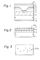
- Figure 1 shows a V-grooved substrate buried hetero structure (VSB) of an LD.
- an n type indium phosphorus (InP) substrate 1 has formed on it an n type InP buffer layer 2, P type InP block layer 3, n type InP block layer 4, InGaAsP active layer 5, P type InP clad layer 6, and P type InGaAsP contact layer 7, in that order. Further, the upper surface of the contact layer 7 and the lower surface of the substrate 1 have respectively formed thereon metal electrodes 8 and 9 ohmically contacting thereto.
- InP indium phosphorus
- the uppermost semiconductor layer is usually a contact layer of InGaAsP into which the concentration of impurities can be increased as explained above. Since the concentration of impurities cannot be sufficiently increased in InP, InP cannot be used as a contact layer.
- the qualities of the respective semiconductor layers including the InGaAsP contact layer determine the lifetime of the semiconductor light emitting device.
- the semiconductor layers formed on the substrate 1 are made of compound semiconductors.
- the semiconductor layers of compound semiconductors are usually formed by a liquid phase epitaxial process.
- an InGaAsP contact layer 7 is formed by the liquid phase epitaxial process as the uppermost layer of the semiconductor layer.
- indium particles 10a are left as shown in Figs. 2 and 3. If the indium particles are large, they can be removed by using, for example, a cloth buff. However, it was found by the inventor that the very small indium particles 10a left on the InGaAsP contact layer 7 cannct be removed thereby.
- an electrode 8 is formed on the InGaAsP contact layer 7 having small indium particles 10a.thereon, the lifetime of the semiconductor light emitting device is reduced due to the small indium particles positioned between the InGaAsP contact layer 7 and the electrode 8.
- Japanese Unexamined Patent Publication No. 55-55522 discloses a liquid phase epitaxial process in which, after forming an upper semiconductor layer of, for example, InGaAsP or InP, an additional layer of InP or InGaAsP different from the upper semiconductor layer is formed to melt indium left thereon and, after cooling, the additional layer of InP or InGaAsP is etched by well known different etchants without removing the indium particles.
- indium newly left on the additional layer of InP is still left on the upper semiconductor layer even after etching the InP using a well known etchant, for example, HC1 or HBr. Namely, although InP can be easily melted by the etchant, indium cannot be easily melted thereby.
- a well known etchant for example, HC1 or HBr.
- Figures 4A to 4C show cross-sectional views of steps in a method embodying the present invention.
- Layers 2, 3, 4, and 5 are conventionally formed on an InP substrate 1 and after a p type clad layer 6 (having a thickness of about 1 ⁇ m) is formed on the layer 5, a p type InGaAsP contact layer 7 (having a thickness of about 0.5 ⁇ m) is formed while indium particles are left thereon due to the wave state of the surface thereof.
- an I nP cover layer 11 (having a thickness of about 0.5 ⁇ m) is formed on the p type InGaAsP contact layer 7 by the liquid phase epitaxial process.
- the surface of the InP cover layer 11 is flushed or cleaned for example with a mixed solution of HF and HNO 3 (mixed ratio 1:1).
- a mixed solution of HF and HNO 3 mixed ratio 1:1.
- the InP cover layer 11 on the InGaAsP contact layer 7 can be selectively removed by an etching process for example using HCl or HBr as an etchant so that the previously formed contact layer 7 is exposed.
- an etching process for example using HCl or HBr as an etchant.
- the inventor found by using an optical microscope that no indium particles were seen on the InGaAsP contact layer 7.
- InGaAsP-InP-In particles are used in the present invention.
- indium particles are selectively removed by a mixed solution of HF and HN0 3 .
- InP is selectively removed by HC1 or HBr, with the result that indium particles left on the InGaAsP can be removed.
- FIG. 5 is a graph indicating the lifetime of light emitting devices of the prior art and the present invention.
- the cleaning solution used for selectively melting (dissolving) particles of Indium may be a selective etching solution (etchant).
Landscapes
- Semiconductor Lasers (AREA)
- Led Devices (AREA)
- Liquid Deposition Of Substances Of Which Semiconductor Devices Are Composed (AREA)
- Weting (AREA)
Applications Claiming Priority (2)
| Application Number | Priority Date | Filing Date | Title |
|---|---|---|---|
| JP277539/84 | 1984-12-26 | ||
| JP59277539A JPS61154091A (ja) | 1984-12-26 | 1984-12-26 | 半導体発光素子の製造方法 |
Publications (2)
| Publication Number | Publication Date |
|---|---|
| EP0186461A2 true EP0186461A2 (fr) | 1986-07-02 |
| EP0186461A3 EP0186461A3 (fr) | 1988-09-14 |
Family
ID=17584960
Family Applications (1)
| Application Number | Title | Priority Date | Filing Date |
|---|---|---|---|
| EP85309307A Withdrawn EP0186461A3 (fr) | 1984-12-26 | 1985-12-20 | Méthode pour fabriquer un dispositif émetteur de lumière à semi-conducteur |
Country Status (4)
| Country | Link |
|---|---|
| US (1) | US4686001A (fr) |
| EP (1) | EP0186461A3 (fr) |
| JP (1) | JPS61154091A (fr) |
| KR (1) | KR890004482B1 (fr) |
Families Citing this family (3)
| Publication number | Priority date | Publication date | Assignee | Title |
|---|---|---|---|---|
| KR900013612A (ko) * | 1989-02-17 | 1990-09-05 | 프레데릭 얀 스미트 | 두 물체의 연결 방법 및 장치 |
| US5641381A (en) * | 1995-03-27 | 1997-06-24 | The United States Of America As Represented By The Administrator Of The National Aeronautics And Space Administration | Preferentially etched epitaxial liftoff of InP material |
| US5772907A (en) * | 1996-05-08 | 1998-06-30 | The United States Of America As Represented By The Secretary Of The Navy | Lactic acid treatment of InP materials |
Family Cites Families (3)
| Publication number | Priority date | Publication date | Assignee | Title |
|---|---|---|---|---|
| JPS5116286A (en) * | 1974-03-25 | 1976-02-09 | Oki Electric Ind Co Ltd | Gsp kyomenetsuchingueki |
| JPS5555522A (en) * | 1978-10-19 | 1980-04-23 | Fujitsu Ltd | Method of epitaxial growth at liquid phase |
| DE3222790A1 (de) * | 1982-06-18 | 1983-12-22 | Wacker-Chemitronic Gesellschaft für Elektronik-Grundstoffe mbH, 8263 Burghausen | Verfahren zum polieren von indiumphosphidoberflaechen |
-
1984
- 1984-12-26 JP JP59277539A patent/JPS61154091A/ja active Granted
-
1985
- 1985-12-20 EP EP85309307A patent/EP0186461A3/fr not_active Withdrawn
- 1985-12-23 US US06/812,656 patent/US4686001A/en not_active Expired - Fee Related
- 1985-12-24 KR KR1019850009760A patent/KR890004482B1/ko not_active Expired
Also Published As
| Publication number | Publication date |
|---|---|
| KR860005453A (ko) | 1986-07-23 |
| JPH0144031B2 (fr) | 1989-09-25 |
| KR890004482B1 (ko) | 1989-11-04 |
| US4686001A (en) | 1987-08-11 |
| EP0186461A3 (fr) | 1988-09-14 |
| JPS61154091A (ja) | 1986-07-12 |
Similar Documents
| Publication | Publication Date | Title |
|---|---|---|
| US20070093026A1 (en) | Method of Making Thin Silicon Sheets for Solar Cells | |
| JP2008211228A (ja) | 窒化物系半導体素子の製造方法 | |
| WO1994024341A1 (fr) | Procede ameliore d'arrachement de couches epitaxiales | |
| KR20000023446A (ko) | 에피택셜웨이퍼 및 그 제조방법 및 그것에 사용되는화합물반도체기판의 표면청정화방법 | |
| US5766976A (en) | Method for detecting crystal defects in a silicon single crystal substrate | |
| EP0186461A2 (fr) | Méthode pour fabriquer un dispositif émetteur de lumière à semi-conducteur | |
| US4994143A (en) | Method for manufacturing a buried heterostructure laser diode | |
| US6864112B1 (en) | Method of production of a patterned semiconductor layer | |
| GB2156585A (en) | Light-emitting device electrode | |
| JP2008192663A (ja) | 半導体素子の製造方法 | |
| CN102623579A (zh) | 半导体发光芯片制造方法 | |
| JP2021064719A (ja) | 光半導体装置の製造方法 | |
| JP2710248B2 (ja) | 半導体レーザの製造方法 | |
| KR100586609B1 (ko) | 질화갈륨계 발광 소자의 제조 방법 | |
| JPH04249384A (ja) | 半導体発光素子の製造方法 | |
| JP7639779B2 (ja) | 受光素子の製造方法 | |
| JP2010027670A (ja) | 半導体構造の加工方法 | |
| CA1139411A (fr) | Fabrication simultanee de diodes electroluminescentes et de diodes laser a double heterostructure par epitaxie en phase liquide | |
| JPS59232475A (ja) | 半導体素子の製造方法 | |
| KR940008178A (ko) | 매립형 반도체 레이저 다이오드 | |
| JP3487282B2 (ja) | 化合物半導体の電極製造方法 | |
| JP2004128279A (ja) | 半導体装置の製造方法 | |
| RU2146842C1 (ru) | Способ изготовления полупроводникового светоизлучающего элемента | |
| JPH05109694A (ja) | 半導体結晶の処理方法 | |
| JPS61281561A (ja) | 半導体面発光素子の製造方法 |
Legal Events
| Date | Code | Title | Description |
|---|---|---|---|
| PUAI | Public reference made under article 153(3) epc to a published international application that has entered the european phase |
Free format text: ORIGINAL CODE: 0009012 |
|
| AK | Designated contracting states |
Kind code of ref document: A2 Designated state(s): DE FR GB |
|
| PUAL | Search report despatched |
Free format text: ORIGINAL CODE: 0009013 |
|
| AK | Designated contracting states |
Kind code of ref document: A3 Designated state(s): DE FR GB |
|
| 17P | Request for examination filed |
Effective date: 19890228 |
|
| 17Q | First examination report despatched |
Effective date: 19900802 |
|
| STAA | Information on the status of an ep patent application or granted ep patent |
Free format text: STATUS: THE APPLICATION IS DEEMED TO BE WITHDRAWN |
|
| 18D | Application deemed to be withdrawn |
Effective date: 19930803 |
|
| RIN1 | Information on inventor provided before grant (corrected) |
Inventor name: OKAZAKI, NIRO |