EP0186462A2 - Dekodierungsverfahren für Manchester-kodierte Signale - Google Patents
Dekodierungsverfahren für Manchester-kodierte Signale Download PDFInfo
- Publication number
- EP0186462A2 EP0186462A2 EP85309310A EP85309310A EP0186462A2 EP 0186462 A2 EP0186462 A2 EP 0186462A2 EP 85309310 A EP85309310 A EP 85309310A EP 85309310 A EP85309310 A EP 85309310A EP 0186462 A2 EP0186462 A2 EP 0186462A2
- Authority
- EP
- European Patent Office
- Prior art keywords
- signal
- input
- gate
- receives
- flop
- Prior art date
- Legal status (The legal status is an assumption and is not a legal conclusion. Google has not performed a legal analysis and makes no representation as to the accuracy of the status listed.)
- Granted
Links
- 238000001514 detection method Methods 0.000 title claims abstract description 20
- 238000000034 method Methods 0.000 title claims abstract description 18
- 230000000694 effects Effects 0.000 claims abstract description 39
- 238000005070 sampling Methods 0.000 claims description 9
- 230000007704 transition Effects 0.000 claims description 9
- 238000012544 monitoring process Methods 0.000 abstract description 2
- 238000007781 pre-processing Methods 0.000 abstract description 2
- 238000011084 recovery Methods 0.000 description 18
- 230000000295 complement effect Effects 0.000 description 16
- 238000010586 diagram Methods 0.000 description 15
- 230000005540 biological transmission Effects 0.000 description 8
- 230000003139 buffering effect Effects 0.000 description 8
- 101100082028 Arabidopsis thaliana PLL2 gene Proteins 0.000 description 7
- 101100350628 Arabidopsis thaliana PLL3 gene Proteins 0.000 description 7
- 238000012797 qualification Methods 0.000 description 6
- 238000004891 communication Methods 0.000 description 4
- 230000001360 synchronised effect Effects 0.000 description 4
- 238000010168 coupling process Methods 0.000 description 3
- 238000005859 coupling reaction Methods 0.000 description 3
- 230000004044 response Effects 0.000 description 3
- 230000000630 rising effect Effects 0.000 description 3
- 230000008859 change Effects 0.000 description 2
- 230000008878 coupling Effects 0.000 description 2
- 230000003111 delayed effect Effects 0.000 description 2
- 238000002955 isolation Methods 0.000 description 2
- 230000011664 signaling Effects 0.000 description 2
- 101100350613 Arabidopsis thaliana PLL1 gene Proteins 0.000 description 1
- 230000015572 biosynthetic process Effects 0.000 description 1
- 238000013461 design Methods 0.000 description 1
- 101150110946 gatC gene Proteins 0.000 description 1
- 238000012545 processing Methods 0.000 description 1
- 230000035755 proliferation Effects 0.000 description 1
- 230000000644 propagated effect Effects 0.000 description 1
- 238000003786 synthesis reaction Methods 0.000 description 1
Images


Classifications
-
- H—ELECTRICITY
- H03—ELECTRONIC CIRCUITRY
- H03M—CODING; DECODING; CODE CONVERSION IN GENERAL
- H03M5/00—Conversion of the form of the representation of individual digits
- H03M5/02—Conversion to or from representation by pulses
- H03M5/04—Conversion to or from representation by pulses the pulses having two levels
- H03M5/06—Code representation, e.g. transition, for a given bit cell depending only on the information in that bit cell
- H03M5/12—Biphase level code, e.g. split phase code, Manchester code; Biphase space or mark code, e.g. double frequency code
Definitions
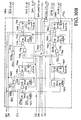
- a third D-type flip-flop 418 receives at its data input (D) the signal generated by an OR gate 420 which, in turn, receives at a first input the IARST signal generated by flip-flop 404.
- a second input of OR gate 420 receives the signal generated at the output terminal of MUX 414.
- Flip-flop 418 also receives the CLK16 signal at its clock input.
- a third two-in, one-out multiplexer (MUX) 422 receives at a control input (SO) the signal generated by an OR gate 424 which, in turn, receives at a first input the signal generated at the output terminal (Q) of flip-flop 410.
- a PLLO D-type flip-flop 536 receives at its data input (D) the signal generated by an OR gate 537 which, in turn, receives at a first input the CRESET signal.
- a second input of OR gate 537 receives the signal generated at the output terminal of MUX 532.
- Flip-flop 536 also receives the CLK16 signal at its clock input. The signal generated at the complemented output terminal ( Q) of flip-flop 536 is conducted to a true (10) and a complemented (1D) input terminal of MUX 532.
- a second input of OR gate 544 receives the signal generated at the output terminal of MUX 538.
- Flip-flop 542 also receives the CLK16 signal at its clock input.
- the signal generated at the complemented output terminal ( Q) of flip-flop 542 is conducted to a true (1Q) and a complemented (1D) input terminal of MUX 538.
- a fifth two-in, one-out multiplexer (MUX) 562 receives at a control input (SO) the signal generated by an OR gate 564 which, in turn, receives at a first input the signal generated at the complemented output terminal ( Q) of flip-flop 536.
- a second input of OR gate 512 receives the signal generated at the output terminal (Q) of flip-flop 542.
- the control signal is used by the MUX 510 to select which of the signals applied to MUX 510 at a 1Q or a complemented 1D terminal will be generated at an output of MUX 510.
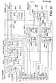
- OR gate 600 The output terminal of OR gate 600 is connected to a first input terminal of an AND gate 602, which in turn has its output terminal connected to a first input terminal of an OR gate 604.
- OR gate 604. generates at its output terminal a signal received at a data (D) input terminal of a LENGTHEN D-type flip-flop 606.
- Flip-flop 606 receives at its clock input terminal the CLK16 signal and generates at its true (Q) output terminal a LENGTHEN signal which is conducted to a second input terminal of , ⁇ ND gate 602 and to a second input terminal of an AND gate 586.
- a second input terminal of OR gate 604 receives the setreset (SRST) signal generated at the true output terminal of AND gate 588.
- Flip-flop 616 receives the CLK16 signal at its clock input terminal.
- a third buffering D-type flip-flop 618 receives at its data input (D) the DATO signal generated at the true (Q) output terminal of flip-flop 616, as well as the CLK16 signal at its clock input terminal.
- OR gate 638 The output terminal of OR gate 638 is connected to the data (D) input terminal of a D-type flip-flop 640 which generates at its true (Q) and complemented output terminals an RSUPO, and RSUPO signals, respectively.
- Flip-flop 640 also receives the CLK 16 signal at its clock input terminal.
- MUX 636 receives at a control (SO) the RSUPO signal, which signal is used by the MUX 636 to select which of the signals applied to MUX 636 at its 1Q or ID terminals will be generated at its output terminal.
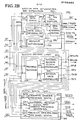
- block 130 of receiver 100 includes a data cell status decoder portion 668 (139 on Fig. 2B) which includes the aforementioned OR gate 652.
- Gate 652 receives at a second input terminal the IACP signal and at a third input terminal the signal generated at the output terminal of a NAND gate 670 which, in turn, receive the signal generated at the output of OR gates 672 and 674.
- OR gate 672 receives the VAL, OVAL and DATO signals;
- OR gate 674 receives the DATO, VAL and OVAL signals.
- An AND gate 676 receives the signal generated by OR gate 652 and the 1/4 signal, and generates therefrom the EOM@I/4 signal, which is conducted to a second input terminal of OR gate 650 as well as to the Receive Decode Logic block 140.
- Portion 668 also includes an XOR gate 678 which receives the VAL and OVAL signals and generates therefrom a DATA/FAULT and a DATA/FAULT signal at its true and complemented output terminal, respectively.
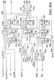
- Receive Decode Logic block 140 of Receiver 100 is shown in Figs. 10A and lOB.
- a preamble detector portion 700 (142 on Fig. 2B) is shown in Fig. 10A, which receives the CLK16, EOM@1/4, 1/4, DATA, DATA, and VAL signals described earlier in connection with blocks 110, 120, 130 and 150 of Receiver 100, and the IMODE signal to be described hereinafter.
- a set of three flip-flops 702, 704, and 706 provide a three inter-bit delay by generating at their true (Q), and complement ( Q), outputs preamble detector timing signals PD2 and PD2, PD1 and PD1, PDO and PDO, respectively. As shown in Fig.
- flip-flops 702, 704 and 706 receive at their data (D) input terminals the signals generated an OR gate 708, 710, 712, respectively, which, in turn, receive at a first input the EOM@1/4 signal and at a second input the signal generated at an output of a two-in, one-out multiplexer (MUX) 714, 716, 718, respectively.
- MUX two-in, one-out multiplexer
- Flip-flops 702, 704, and 706 receive the CLK16 signal at their clock inputs.
- MUX 714, 716 and 718 each receive at a control input (SO) the IMODE signal, which signal is used by the MUX to which of the signals applied at their 1Q or 1D terminals will be generated at their respective output terminals.
- MUX 714 and 716 receive at their 1D input terminals the output generated at the Q, respectively, Q, output terminal of flip-flop 702, 706, respectively.
- a two-in, one output MUX 720, 722, respectively, generate at their output terminals a signal received at a first input terminal of an OR gate 724, 726, respectively, which in turn, generates a signal received at the 1D, 10, respectively, input terminal of MUX 714, 718, respectively.
- the signal generated at the Q output terminal of flip-flop 706 is received at the true (10) and complemented (1D) input terminals of NUX 722, and the signal generated at the Q output terminal of flip-flop 706 is received at the 1D input terminal of MUX 718.
- MUX 720, 722, respectively, receives at its control input (SO) the output signal generated by an OR gate 728, 730, respectively, receiving, in turn the PD1 and PDO signals, the PDO, P1 and PD2 signals, respectively.
- the MUX 716 receives at its 10 input terminal the signal generated by an OR gate 732.
- OR gate 732 receives at a first input terminal the signal generated by an AND gate 734 which, in turn, receives at a first input terminal the signal generated by an OR gate 736 which receives the DATA and PD2 signals and at second complemented input terminal the signal generated by an OR gate 738 which receives the PD1, PD2, DATA signals and the signal generated by an XOR gate 740.
- XOR gate turn, receives the PDO and VAL signals.
- the DATA and VAL signals are received by an OR gate 742 which generates therefrom a signal conducted to a first input terminal of an AND gate which receives the PD2 signal at a second input terminal.
- the signal generated by AND gate 744 is conducted to a second input terminal of OR gates 724 and 726.
- Section 750 also includes an OR gate 772 which receives at a first input terminal the DC1 signal generated by flip-flop 770 and generates at a true output terminal a signal received at a first input terminal of an OR gate 774 which, in turn, generates a signal received by the 10 input of MUX 770.
- OR gate 774 receives at a second input terminal the signal generated by an AND gate 776 which receives at a first input the DATA signal and at a second input the signal generated by an OR gate 778 which, in turn, receives the CP1 and CP2 signals.
- OR gate 772 generated at a complemented output terminal the DEN signal.
- Output Synthesizer block 160 of Receiver 160 is shown on Fig. 11; consisting of an Advanced Carrier Presence Synthesizer portion 800 (162 on Fig. 2B), an External Receive clock and Carrier presence synthesis portion 802 (164 on Fig. 2B) and a Receive Data and Carrier Sense Synthesizer portion 804 (166 on Fig. 2B).
- Portion 804 includes a D-type flip-flop 834 which receives at its data (D) input the signal generated by an OR gate 836 which, in turn, receives the RESET signal and the signal generated at the complemented output terminal of an XOR gate 838 receiving the DCO and DC1 signals.
- Flip-flop 834 receives the CLK16 signal at its clock input terminal.
- Flip-flop 834 generates at its Q output terminal the complemented carrier sense ( CS) signal.
- Portion 804 also includes a two-input, one-output MUX 840 which receives at its control input (SO) the 3/4 signal; which signal is used by the MUX 840 to select which of the signals applied at a 1Q or a 1D terminal will be generated at an output of MUX 840.
- SO control input
- a second internal signal is advanced carrier sense (ACS) which indicates if the line activity which caused the Receiver 100 to set IACP HIGH is valid Manchester-encoded data.
- the Receiver 100 sets ACS HIGH if the detected line signal has a differential voltage greater than the positive carrier presence level followed within a window of 3/4 to 1 1/4 bit times by a voltage less than the negative carrier presence level, or if the line signal has a differential voltage less than the negative carrier presence level followed within the window by a voltage greater than the positive carrier presence level.
- the ACS signal is set HIGH only when IACP is HIGH or during the first clock interval after IACP has been set low.
- An edge (EDGE) internal signal is set HIGH whenever the Receiver 100 detects a zero-crossing by the input line data.
- a clock recovery preset (CRESET) signal is set HIGH for one clock cycle following the next line data edge (EDGE HIGH) after the line activity is detected, (IACP HIGH), and the data qualification is complete (ACS HIGH).
- CRESET is set HIGH once during reception of input line data by Receiver 100.
- a line acquisition (LA) signal is set HIGH following CRESET set HIGH until a physical (line quiet) or logical (decoded) end-of-message.
- the data-sampling signals 1/4 and 3/4 are used to determine whether the line input data is valid Manchester-encoded.
- the line data is sampled at a 1/4 and a 3/4 interval from the start of an inter-bit time interval.
- a DATA signal is set HIGH if the decoded line data is valid Manchester-encoded based on the opposite logical polarity at the 1/4 and 3/4 sample-times.
- a logical end-of-message (EOM@1/4) is set HIGH whenever no line activity is detected and will be reset low when CRESET is set HIGH and will remain low until the logical end of message or LA is set low.
- the Receiver 100 is in an OFF state, 300.
- the Receiver channel interface 10 has not generated ST+ or ST- signals which satisfy the conditions described above calling for generation of the HIGH IACP signal.
- no output signals are generated at the Receiver 100 output terminals RxC or RxD, and the recovered clock oscillator portion of block 150 is asynchronous.
- the detection at the channel interface 10 of line activity will cause Receiver 100 to generate a HIGH IACP signal and upon detection of valid Manchester-encoded input data, the ACS signal is set HIGH and the Supervisor changes to ENABLE state, 302. If line activity is detected but Manchester-encoded input data is not detected, ACS will remain inactivated LOW and the Receiver 100 will remain in the OFF state, 300.
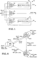
- the Receiver 100 detects valid Manchester-encoded data applied to the RxLO, RxLl terminals by first generating at the Receiver channel interface 10 the ST+, ST- and INPUT DATA signals described above in connection with FIGS. 1 and 3.
- Receiver 100 contains an internal clock (not . shown in FIG. 2) having a frequency sixteen times the int y r-bit frequency of the bit stream (16x clock) applied to the RxLO, RxLl terminals.
- VCO voltage-controlled oscillator
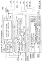
- the flip-flop 114 storing the ALS signal is clocked and a HIGH complement signal IARST is generated therefrom and applied to reset a 2-bit line active time-out counter 116 internal to block 110 and to set a flip-flop 118 (440 on Fig. 6) connected to the counter 116 which generates a HIGH internal ACP (IACP) signal.
- IACP HIGH internal ACP
- a register 129 (472 on Fig. 7) internal to block 120 receives the IACP signal and the double-buffered ST+, ST- signals and supplies a third input to OR gate 125 which generates a HIGH signal when IACP is a LOW thereby resetting the counter 126 and ensuring that the first-generated ACS signal, the only one used, is correct.
- the INPUT DATA signals generated by the differential zero-crossing detector 16 of receiver channel interface 10 are applied to an input data synchronizer portion 132 of the Receive Data Interpreter and Supervisor block 130 (610 on Fig. 9) of receiver 100.
- Data synchronizer 132 includes two buffering flip-flops 612 and 616 which receive the LINE INPUT DATA signals and synchronizes the signals with the internal clock applied to the flip-flops.
- the complement output of the second buffering flip-flop 616 ( DATO) is received by a data zero-crossing detector portion 134 (622 on Fig. 9) of block 130.
- An OR gate 614 is connected to the input of the first buffering flip-flop of data synchronizer 132 and receives the IACP signal as well as the LINE INPUT DATA signals thereby ensuring that the EDGE signal is inactive whenever IACP is inactive.
- the Receive Supervisor 136 receives the DPPLON signal generated by the Receive Decode Logic 140 block, as will be explained below, and this signal is applied to an OR gate 626, which also receives the IACP signal generated by the Receive Line Activity Counter 110.
- the output of this OR gate is conducted to the input of the first delay flip-flop 630 within the receive supervisor 136 and thereby permits the supervisor to return to the OFF "00" state from the FORCE "10" state only when no line activity is detected (IACP LOW) and the receiver 100 has effected logical external output signal completion (DPLLON LOW).
- the EOM@1/4 signal is also generated within cell sampler 138 by applying the VAL and OVAL signals and their complements generated by the delay flip-flops 662 and 664 within cell sampler 138 to a pair of OR gates 672 and 674 which are in turn connected to a NAND gate 670 the output of which is applied to a second OR gate 652.
- the latter OR gate also receiving the IACP and LA signals described above.
- the output of the latter OR gate is conducted to an AND gate 676 which also receives the 1/4 sampling signal.
- the signal generated by the AND gate 676 being the EOM@1/4 signal described above.
- the CP1 signal is conducted to an external receive clock controller portion 144 (750 on Fig. 10B)of block 140 which also receives the IMODE signal and the 1/4-sample signal.
- the external receive clock controller 144 generates a HIGH DPLLON signal on the reception of a HIGH 1/4-sample signal following detection of the preamble after the HIGH CRESET signal is received by preamble detector 142 which accordingly generates a HIGH CP2 signal.
- IMODE LOW when the CP1 signal received from preamble detector 142 becomes a HIGH DPI signal is generated by clock controller 144 which is transmitted to an output snythesizer block 160 where it causes signals at the CP and RxC output terminals of receiver 100 to be generated.
- a DPO signal is immediately generated by clock controller 144 which is transmitted to block 160 and causes signals at the CP and RxC output terminals to be immediately generated.
- preamble detector 142 If preamble was detected and preamble detector 142 generated a HIGH CP2 signal, but the first data signal after the preamble caused a HIGH DATA/FAULT signal to be generated, the signal at the RxD output terminal is activated, but the signal at the CS output terminal is removed after the first RxC cycle.
- the output synthesizer block 160 receives the IACP, DPLLON, 1/4 sample, 3/4 sample, DCO, DC1, DPO, DP1, VAL and DEN signals generated by the blocks 110, 120, 130, 140 and 150 as previously described.
- An advanced carrier presence synthesizer portion 162 (800 on F i g. 11) generates an IEACP signal from the IACP, and DPLLON signals so that a HIGH IACP signal can generate a HIGH IEACP signal and LOW IACP and DPLLON signals cause a LOW IEACP signal to be generated.
Landscapes
- Engineering & Computer Science (AREA)
- Theoretical Computer Science (AREA)
- Dc Digital Transmission (AREA)
- Synchronisation In Digital Transmission Systems (AREA)
- Radar Systems Or Details Thereof (AREA)
Priority Applications (1)
| Application Number | Priority Date | Filing Date | Title |
|---|---|---|---|
| AT85309310T ATE64045T1 (de) | 1984-12-21 | 1985-12-20 | Dekodierungsverfahren fuer manchester-kodierte signale. |
Applications Claiming Priority (2)
| Application Number | Priority Date | Filing Date | Title |
|---|---|---|---|
| US06/684,085 US4606052A (en) | 1984-12-21 | 1984-12-21 | Method for detection of line activity for Manchester-encoded signals |
| US684085 | 1984-12-21 |
Publications (3)
| Publication Number | Publication Date |
|---|---|
| EP0186462A2 true EP0186462A2 (de) | 1986-07-02 |
| EP0186462A3 EP0186462A3 (en) | 1988-09-14 |
| EP0186462B1 EP0186462B1 (de) | 1991-05-29 |
Family
ID=24746623
Family Applications (1)
| Application Number | Title | Priority Date | Filing Date |
|---|---|---|---|
| EP85309310A Expired - Lifetime EP0186462B1 (de) | 1984-12-21 | 1985-12-20 | Dekodierungsverfahren für Manchester-kodierte Signale |
Country Status (5)
| Country | Link |
|---|---|
| US (1) | US4606052A (de) |
| EP (1) | EP0186462B1 (de) |
| JP (1) | JPS61199355A (de) |
| AT (1) | ATE64045T1 (de) |
| DE (1) | DE3583011D1 (de) |
Cited By (1)
| Publication number | Priority date | Publication date | Assignee | Title |
|---|---|---|---|---|
| EP0304799A3 (en) * | 1987-08-27 | 1990-06-20 | Deutsche Thomson-Brandt Gmbh | Method and/or apparatus for demodulating a biphase signal |
Families Citing this family (23)
| Publication number | Priority date | Publication date | Assignee | Title |
|---|---|---|---|---|
| US4862482A (en) * | 1988-06-16 | 1989-08-29 | National Semiconductor Corporation | Receiver for Manchester encoded data |
| US5023891A (en) * | 1989-07-25 | 1991-06-11 | Sf2 Corporation | Method and circuit for decoding a Manchester code signal |
| US5179577A (en) * | 1991-06-06 | 1993-01-12 | Digital Equipment Corporation | Dynamic threshold data receiver for local area networks |
| US5742847A (en) * | 1994-10-31 | 1998-04-21 | Intel Corporation | M&A for dynamically generating and maintaining frame based polling schedules for polling isochronous and asynchronous functions that guaranty latencies and bandwidths to the isochronous functions |
| US5621901A (en) * | 1994-10-31 | 1997-04-15 | Intel Corporation | Method and apparatus for serial bus elements of an hierarchical serial bus assembly to electrically represent data and control states to each other |
| US5623610A (en) * | 1994-10-31 | 1997-04-22 | Intel Corporation | System for assigning geographical addresses in a hierarchical serial bus by enabling upstream port and selectively enabling disabled ports at power on/reset |
| US5615404A (en) * | 1994-10-31 | 1997-03-25 | Intel Corporation | System having independently addressable bus interfaces coupled to serially connected multi-ported signal distributors generating and maintaining frame based polling schedule favoring isochronous peripherals |
| WO1996013776A1 (en) * | 1994-10-31 | 1996-05-09 | Intel Corporation | M & a for exchanging data, status, and commands over a hierarchical serial bus assembly using communication packets |
| US6108237A (en) * | 1997-07-17 | 2000-08-22 | Micron Technology, Inc. | Fast-sensing amplifier for flash memory |
| US5682496A (en) * | 1995-02-10 | 1997-10-28 | Micron Quantum Devices, Inc. | Filtered serial event controlled command port for memory |
| KR100461922B1 (ko) * | 1995-11-13 | 2005-05-24 | 텍사스 인스트루먼츠 인코포레이티드 | 맨체스터코드화데이터와같은잡음성,단속성데이터를디코딩하는방법및장치 |
| US6128112A (en) * | 1996-08-22 | 2000-10-03 | Mcdonnell Douglas Corporation | Weighted-sum processing method and apparatus for decoding digital signals |
| US5694231A (en) * | 1996-08-22 | 1997-12-02 | Mcdonnell Douglas Corporation | Weighted-sum processing method and apparatus for decoding optical signals |
| US5939905A (en) * | 1996-09-27 | 1999-08-17 | Texas Instruments Incorporated | Loop control detection circuit and method for detecting current feedback |
| DE69814822T2 (de) * | 1997-12-22 | 2004-04-08 | Koninklijke Philips Electronics N.V. | Zeitdiskreter phasenregelkreis |
| US7170949B2 (en) | 2002-03-14 | 2007-01-30 | Intel Corporation | Methods and apparatus for signaling on a differential link |
| JP4145583B2 (ja) * | 2002-07-02 | 2008-09-03 | シャープ株式会社 | 信号伝送方法、信号伝送システム、論理回路、及び液晶駆動装置 |
| TWI234374B (en) * | 2003-03-04 | 2005-06-11 | Realtek Semiconductor Corp | Spread spectrum encoding method and spread spectrum encoding modulation method |
| US7627029B2 (en) | 2003-05-20 | 2009-12-01 | Rambus Inc. | Margin test methods and circuits |
| US7590175B2 (en) | 2003-05-20 | 2009-09-15 | Rambus Inc. | DFE margin test methods and circuits that decouple sample and feedback timing |
| US7697651B2 (en) * | 2004-06-30 | 2010-04-13 | Intel Corporation | Lock system and method for interpolator based receivers |
| US20080118016A1 (en) * | 2006-11-20 | 2008-05-22 | Yu-Min Chuang | Synchronous circuit of receiving device of wireless transmission system |
| US9484949B1 (en) | 2015-04-09 | 2016-11-01 | Oracle International Corporation | Variable run length encoding of a bit stream |
Family Cites Families (4)
| Publication number | Priority date | Publication date | Assignee | Title |
|---|---|---|---|---|
| US3243580A (en) * | 1960-12-06 | 1966-03-29 | Sperry Rand Corp | Phase modulation reading system |
| US3244986A (en) * | 1962-10-08 | 1966-04-05 | Ibm | Detection of bi-phase digital signals |
| US3836956A (en) * | 1972-12-12 | 1974-09-17 | Robertshaw Controls Co | Method and apparatus for decoding biphase signals |
| FR2275084A1 (fr) * | 1974-06-12 | 1976-01-09 | Siemens Ag | Procede de transmission de donnees a synchronisme de bits |
-
1984
- 1984-12-21 US US06/684,085 patent/US4606052A/en not_active Expired - Lifetime
-
1985
- 1985-12-20 EP EP85309310A patent/EP0186462B1/de not_active Expired - Lifetime
- 1985-12-20 DE DE8585309310T patent/DE3583011D1/de not_active Expired - Lifetime
- 1985-12-20 AT AT85309310T patent/ATE64045T1/de not_active IP Right Cessation
- 1985-12-20 JP JP60289136A patent/JPS61199355A/ja active Granted
Cited By (1)
| Publication number | Priority date | Publication date | Assignee | Title |
|---|---|---|---|---|
| EP0304799A3 (en) * | 1987-08-27 | 1990-06-20 | Deutsche Thomson-Brandt Gmbh | Method and/or apparatus for demodulating a biphase signal |
Also Published As
| Publication number | Publication date |
|---|---|
| EP0186462A3 (en) | 1988-09-14 |
| JPH0545105B2 (de) | 1993-07-08 |
| JPS61199355A (ja) | 1986-09-03 |
| ATE64045T1 (de) | 1991-06-15 |
| US4606052A (en) | 1986-08-12 |
| EP0186462B1 (de) | 1991-05-29 |
| DE3583011D1 (de) | 1991-07-04 |
Similar Documents
| Publication | Publication Date | Title |
|---|---|---|
| US4606052A (en) | Method for detection of line activity for Manchester-encoded signals | |
| EP0185556B1 (de) | Verfahren zur Erzeugung eines digitalen Taktsignals von Manchester-kodierten Signalen | |
| EP0773653B1 (de) | Verfahren und Einrichtung zur Dekodierung von Manchester-kodierten Daten | |
| US5825825A (en) | Method of processing multi-level signals for simple clock recovery | |
| US4167760A (en) | Bi-phase decoder apparatus and method | |
| JPH0661992A (ja) | 位相ロックループ発振器を使用せずに直列に伝送されたデータを回復するための装置および方法 | |
| JPH07115411A (ja) | 集積回路 | |
| US4663767A (en) | Optical data bus having a statistical access method | |
| EP0405968B1 (de) | Taktrückgewinnung für ein serielles Datenkommunikationssystem | |
| US5040193A (en) | Receiver and digital phase-locked loop for burst mode data recovery | |
| US5726650A (en) | Adaptive manchester decoding with adjustable delay and power saving mode | |
| US5123030A (en) | Timing extraction method and communication system | |
| US4905257A (en) | Manchester decoder using gated delay line oscillator | |
| US5267267A (en) | Timing extraction method and communication system | |
| JP2812665B2 (ja) | 通信網のデータ衝突検出回路および検出方法 | |
| JP3087259B2 (ja) | フラッシュnrzi変調装置及び変調方法 | |
| EP0299251B1 (de) | Übertragungsfilter | |
| EP0284164B1 (de) | Dekodierungsgerät für CMI-kodierte Signale | |
| US4694257A (en) | Phase-coherent demodulation clock and data recovery | |
| EP1530820B1 (de) | System für in frequenz kontrollierte signale | |
| US5046073A (en) | Signal processing apparatus for recovering a clock signal and a data signal from an encoded information signal | |
| US4809301A (en) | Detection apparatus for bi-phase signals | |
| JPH104436A (ja) | クロック再生回路 | |
| JP6933258B2 (ja) | 通信回路、通信システム及び通信方法 | |
| CA2185866C (en) | Method of processing multi-level signals for simple clock recovery |
Legal Events
| Date | Code | Title | Description |
|---|---|---|---|
| PUAI | Public reference made under article 153(3) epc to a published international application that has entered the european phase |
Free format text: ORIGINAL CODE: 0009012 |
|
| AK | Designated contracting states |
Kind code of ref document: A2 Designated state(s): AT BE CH DE FR GB IT LI LU NL SE |
|
| PUAL | Search report despatched |
Free format text: ORIGINAL CODE: 0009013 |
|
| AK | Designated contracting states |
Kind code of ref document: A3 Designated state(s): AT BE CH DE FR GB IT LI LU NL SE |
|
| 17P | Request for examination filed |
Effective date: 19881208 |
|
| 17Q | First examination report despatched |
Effective date: 19891211 |
|
| GRAA | (expected) grant |
Free format text: ORIGINAL CODE: 0009210 |
|
| AK | Designated contracting states |
Kind code of ref document: B1 Designated state(s): AT BE CH DE FR GB IT LI LU NL SE |
|
| REF | Corresponds to: |
Ref document number: 64045 Country of ref document: AT Date of ref document: 19910615 Kind code of ref document: T |
|
| REF | Corresponds to: |
Ref document number: 3583011 Country of ref document: DE Date of ref document: 19910704 |
|
| ITF | It: translation for a ep patent filed | ||
| ET | Fr: translation filed | ||
| PGFP | Annual fee paid to national office [announced via postgrant information from national office to epo] |
Ref country code: LU Payment date: 19911204 Year of fee payment: 7 |
|
| PGFP | Annual fee paid to national office [announced via postgrant information from national office to epo] |
Ref country code: BE Payment date: 19911217 Year of fee payment: 7 |
|
| PLBE | No opposition filed within time limit |
Free format text: ORIGINAL CODE: 0009261 |
|
| STAA | Information on the status of an ep patent application or granted ep patent |
Free format text: STATUS: NO OPPOSITION FILED WITHIN TIME LIMIT |
|
| EPTA | Lu: last paid annual fee | ||
| 26N | No opposition filed | ||
| PG25 | Lapsed in a contracting state [announced via postgrant information from national office to epo] |
Ref country code: LU Free format text: LAPSE BECAUSE OF NON-PAYMENT OF DUE FEES Effective date: 19921220 |
|
| PG25 | Lapsed in a contracting state [announced via postgrant information from national office to epo] |
Ref country code: BE Effective date: 19921231 |
|
| BERE | Be: lapsed |
Owner name: ADVANCED MICRO DEVICES INC. Effective date: 19921231 |
|
| EAL | Se: european patent in force in sweden |
Ref document number: 85309310.2 |
|
| PGFP | Annual fee paid to national office [announced via postgrant information from national office to epo] |
Ref country code: AT Payment date: 19971106 Year of fee payment: 13 |
|
| PGFP | Annual fee paid to national office [announced via postgrant information from national office to epo] |
Ref country code: SE Payment date: 19971202 Year of fee payment: 13 |
|
| PGFP | Annual fee paid to national office [announced via postgrant information from national office to epo] |
Ref country code: CH Payment date: 19980109 Year of fee payment: 13 |
|
| PG25 | Lapsed in a contracting state [announced via postgrant information from national office to epo] |
Ref country code: AT Free format text: LAPSE BECAUSE OF NON-PAYMENT OF DUE FEES Effective date: 19981220 |
|
| PG25 | Lapsed in a contracting state [announced via postgrant information from national office to epo] |
Ref country code: SE Free format text: LAPSE BECAUSE OF NON-PAYMENT OF DUE FEES Effective date: 19981221 |
|
| PG25 | Lapsed in a contracting state [announced via postgrant information from national office to epo] |
Ref country code: LI Free format text: LAPSE BECAUSE OF NON-PAYMENT OF DUE FEES Effective date: 19981231 Ref country code: CH Free format text: LAPSE BECAUSE OF NON-PAYMENT OF DUE FEES Effective date: 19981231 |
|
| REG | Reference to a national code |
Ref country code: CH Ref legal event code: PL |
|
| REG | Reference to a national code |
Ref country code: GB Ref legal event code: IF02 |
|
| PGFP | Annual fee paid to national office [announced via postgrant information from national office to epo] |
Ref country code: GB Payment date: 20021104 Year of fee payment: 18 |
|
| PGFP | Annual fee paid to national office [announced via postgrant information from national office to epo] |
Ref country code: NL Payment date: 20021112 Year of fee payment: 18 |
|
| PGFP | Annual fee paid to national office [announced via postgrant information from national office to epo] |
Ref country code: FR Payment date: 20021202 Year of fee payment: 18 |
|
| PGFP | Annual fee paid to national office [announced via postgrant information from national office to epo] |
Ref country code: DE Payment date: 20021230 Year of fee payment: 18 |
|
| PG25 | Lapsed in a contracting state [announced via postgrant information from national office to epo] |
Ref country code: GB Free format text: LAPSE BECAUSE OF NON-PAYMENT OF DUE FEES Effective date: 20031220 |
|
| PG25 | Lapsed in a contracting state [announced via postgrant information from national office to epo] |
Ref country code: NL Free format text: LAPSE BECAUSE OF NON-PAYMENT OF DUE FEES Effective date: 20040701 Ref country code: DE Free format text: LAPSE BECAUSE OF NON-PAYMENT OF DUE FEES Effective date: 20040701 |
|
| GBPC | Gb: european patent ceased through non-payment of renewal fee |
Effective date: 20031220 |
|
| PG25 | Lapsed in a contracting state [announced via postgrant information from national office to epo] |
Ref country code: FR Free format text: LAPSE BECAUSE OF NON-PAYMENT OF DUE FEES Effective date: 20040831 |
|
| NLV4 | Nl: lapsed or anulled due to non-payment of the annual fee |
Effective date: 20040701 |
|
| REG | Reference to a national code |
Ref country code: FR Ref legal event code: ST |