EP0186590A1 - Phasenanschnittsteuerschaltung - Google Patents
Phasenanschnittsteuerschaltung Download PDFInfo
- Publication number
- EP0186590A1 EP0186590A1 EP85402571A EP85402571A EP0186590A1 EP 0186590 A1 EP0186590 A1 EP 0186590A1 EP 85402571 A EP85402571 A EP 85402571A EP 85402571 A EP85402571 A EP 85402571A EP 0186590 A1 EP0186590 A1 EP 0186590A1
- Authority
- EP
- European Patent Office
- Prior art keywords
- network
- linear
- correction
- law
- voltage
- Prior art date
- Legal status (The legal status is an assumption and is not a legal conclusion. Google has not performed a legal analysis and makes no representation as to the accuracy of the status listed.)
- Granted
Links
- 230000010363 phase shift Effects 0.000 claims abstract description 10
- 230000001960 triggered effect Effects 0.000 claims abstract description 4
- 230000001419 dependent effect Effects 0.000 claims description 2
- 239000004065 semiconductor Substances 0.000 description 4
- 238000010586 diagram Methods 0.000 description 3
- 230000007547 defect Effects 0.000 description 2
- 230000002457 bidirectional effect Effects 0.000 description 1
- 230000015572 biosynthetic process Effects 0.000 description 1
- 239000003990 capacitor Substances 0.000 description 1
- 230000000694 effects Effects 0.000 description 1
- 238000012886 linear function Methods 0.000 description 1
- 230000001105 regulatory effect Effects 0.000 description 1
- 230000003068 static effect Effects 0.000 description 1
- 230000007704 transition Effects 0.000 description 1
Images


Classifications
-
- H—ELECTRICITY
- H02—GENERATION; CONVERSION OR DISTRIBUTION OF ELECTRIC POWER
- H02M—APPARATUS FOR CONVERSION BETWEEN AC AND AC, BETWEEN AC AND DC, OR BETWEEN DC AND DC, AND FOR USE WITH MAINS OR SIMILAR POWER SUPPLY SYSTEMS; CONVERSION OF DC OR AC INPUT POWER INTO SURGE OUTPUT POWER; CONTROL OR REGULATION THEREOF
- H02M1/00—Details of apparatus for conversion
- H02M1/08—Circuits specially adapted for the generation of control voltages for semiconductor devices incorporated in static converters
- H02M1/081—Circuits specially adapted for the generation of control voltages for semiconductor devices incorporated in static converters wherein the phase of the control voltage is adjustable with reference to the AC source
Definitions
- the present invention relates to an electronic dimmer control device making it possible to adjust, as a function of a control signal, the power applied to a receiving apparatus by a substantially sinusoidal alternative electrical power source, comprising an electronic controlled switch whose the conductive state is triggered, during each half-wave of the power source, at an instant offering, relative to the end of the previous half-wave, a variable phase shift according to a correction law aimed ensuring the proportionality of the effective power applied to the receiving apparatus and of the value of the control signal on which said phase shift is dependent.
- the operating principle of electronic dimmers or dimmers of this kind is well known; it is based on variable phase control of semiconductors such as triacs or thyristors with respect to the zero crossing of the supply sinusoid.
- This command is generally carried out by means of an electronic circuit commonly known as a trigger, which itself receives information in the form of a variable DC voltage, for example between 0 and 10 V, which makes it possible to have a command between 0 and 100% of the effective output voltage.
- the invention relates to a control device or trigger of the kind defined at the start, in which the phase shift of the instant of tripping of the controlled switch is created in proportion to the value of a continuous signal which varies with the control signal in accordance with said correction law.
- This arrangement is advantageous in that the correction is carried out independently of the voltage of the AC power source (in its form and especially in its amplitude), and this in a static manner, that is to say that 'to a fixed control quantity corresponds a corrected continuous signal also fixed, which allows better control of phenomena and increased precision.
- Said continuous signal is preferably generated, from the control signal, by a function generator providing, thanks to a non-linear network, an approximation by rectilinear connected segments of the correction law.
- the non-linear network is designed to provide the approximation by rectilinear segments only of one of the halves of said curve, while an auxiliary switching network associated with this network allows it to provide the approximation of one and the other of the symmetrical halves. A perfect symmetry of correction is thus obtained on either side of said central point.
- the non-linear network can then comprise a linear section and a non-linear section, while only the non-linear section is switched by the auxiliary network, the linear section naturally playing its role, without switching in the two halves of the curve.
- This auxiliary network can, very simply, be constituted by a bridge of four rectifiers, between two opposite terminals of which is connected the non-linear section of the network, the linear section of the latter being connected between the other opposite terminals of the bridge, which constitute the input and output terminals of the assembly formed by the non-linear network and the auxiliary network.
- Such a non-linear network possibly with the network associated switching, can be implemented as one of the input impedances of an operational amplifier to form with its feedback impedance, consisting of a pure resistance, the desired non-linear correction set.
- the non-linear network with the possibly associated switching network, constitutes a bipolar circuit produced in the form of an interchangeable module with two terminals. This mode. of realization will be particularly appreciated by users wishing to change the correction curve of their dimmers; they can do this without having to change all of these devices.
- a device can comprise a comparator which receives on the one hand a signal from a ramp generator and formed by successive linear ramps starting and ending in synchronism with the half-vibrations of the power source and on the other hand the continuous signal coming from the function generator, and which thus triggers, at the instant when these two signals come to equality, the ignition of the controlled electronic switch.
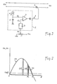
- a power dimmer of the type under consideration essentially comprises (FIG. 1) a controlled switch 1 with semiconductor and a circuit 2 for triggering this switch.
- the controlled switch 1 is placed in series with an electric power source delivering an alternating voltage Ue (generally sinusoidal); it may be a triac, a pair of thyristors mounted head to tail or possibly any other semiconductor device with equivalent bidirectional conduction characteristic.
- the ignition of the switch 1 is triggered by a pulse I generated by the circuit 2 at an instant t of phase variablet variable during each half-period 0 - ⁇ of the voltage Ue of the power source ( Figure 2) .
- each half-wave of the voltage Ue is truncated, so that the output voltage Us, formed of all of these truncated half-waves, has an effective value Ueff varying according to the phase of l 'instant t in the half period.
- This phase is adjustable by applying a variable continuous control voltage Vc to the trigger circuit 2.
- An operational amplifier 4 looped by a resistor R, comprises an input impedance formed by three branches connected in parallel, namely a resistor Ro, a resistor R1 in series with a voltage threshold element E1, and a resistor R2 in series with a voltage threshold element E2 > E1, these last two branches forming the non-linear section of said impedance.
- a voltage Vo is applied to the non-inverting input of the operational amplifier 4.
- the circuit of FIG. 6 is used, which is deduced from that of FIG. 5 essentially by adding a bridge of four diodes D1, D2, D3, D4 intended to ensure the switching of the input voltage Ue so that it attacks in one direction or in the opposite direction, depending on whether Vc is greater or less than Vo, the non-linear bipole formed by the resistors R1 and R2, respectively in series with a diode D5 and a Zener diode Z.
- said bipole is connected between the ends of one of the diagonals of the diode bridge, while the ends of the other diagonal, between which the resistance Ro is connected, constituting the input and output terminals of the corrector network 5 thus formed.
- the voltages E1 and E2 are respectively equal to the forward voltage of the diode D5 and to the Zener voltage of the diode Z, increased by the sum of the forward voltages of the diodes D1 and D3 or of the diodes D2 and D4 according to the value of Vc with respect to Vo.
- the correction network 5 constitutes the input impedance of the operational amplifier 4; to this network is applied, under low impedance via an operational amplifier 6 looped in unity gain, the voltage Vc originating for example from a potentiometer P with linear variation (FIG. 1).
- the network 5 can be in the form of a module with two connection pins, easily interchangeable.
- the voltage V'c delivered by the circuit 3 is applied to one of the inputs of a comparator 7, the other input of which receives a linear sawtooth signal Vt, each of these coinciding with a half-wave of the voltage Ue.
- This signal is generated by a constant current generator i, of invariable value, charging a capacitor C which is discharged periodically at each zero crossing of the voltage Ue.
- a pulse I is produced, which triggers the ignition of the controlled switch 1.
- phase shift of the pulse I in the corresponding half-wave is proportional to the corrected voltage V'c, so that the rms value Ueff of the output voltage Us of the dimmer is constantly proportional to the value of the direct control voltage Vc.
Landscapes
- Engineering & Computer Science (AREA)
- Power Engineering (AREA)
- Circuit Arrangement For Electric Light Sources In General (AREA)
Applications Claiming Priority (2)
| Application Number | Priority Date | Filing Date | Title |
|---|---|---|---|
| FR8419547A FR2575348B1 (fr) | 1984-12-20 | 1984-12-20 | Dispositif de commande de gradateur electronique |
| FR8419547 | 1984-12-20 |
Publications (2)
| Publication Number | Publication Date |
|---|---|
| EP0186590A1 true EP0186590A1 (de) | 1986-07-02 |
| EP0186590B1 EP0186590B1 (de) | 1990-02-28 |
Family
ID=9310830
Family Applications (1)
| Application Number | Title | Priority Date | Filing Date |
|---|---|---|---|
| EP19850402571 Expired - Lifetime EP0186590B1 (de) | 1984-12-20 | 1985-12-20 | Phasenanschnittsteuerschaltung |
Country Status (3)
| Country | Link |
|---|---|
| EP (1) | EP0186590B1 (de) |
| DE (1) | DE3576253D1 (de) |
| FR (1) | FR2575348B1 (de) |
Citations (4)
| Publication number | Priority date | Publication date | Assignee | Title |
|---|---|---|---|---|
| FR1348552A (de) * | 1964-04-10 | |||
| DE2032949A1 (de) * | 1969-12-23 | 1972-01-05 | Marconi Co Lts | Verfahren zur Linearisierung des zeitlichen Mittelwertes einer phasenanschnittgesteuerten Wechselspannung mit dem Steuerwinkel |
| US3942041A (en) * | 1973-10-18 | 1976-03-02 | Atmos Corporation | Thyristor control circuit |
| EP0028890A1 (de) * | 1979-11-05 | 1981-05-20 | Westinghouse Electric Corporation | Digitaler Torimpulsgenerator für ruhende Leistungsumformer |
-
1984
- 1984-12-20 FR FR8419547A patent/FR2575348B1/fr not_active Expired
-
1985
- 1985-12-20 DE DE8585402571T patent/DE3576253D1/de not_active Expired - Fee Related
- 1985-12-20 EP EP19850402571 patent/EP0186590B1/de not_active Expired - Lifetime
Patent Citations (4)
| Publication number | Priority date | Publication date | Assignee | Title |
|---|---|---|---|---|
| FR1348552A (de) * | 1964-04-10 | |||
| DE2032949A1 (de) * | 1969-12-23 | 1972-01-05 | Marconi Co Lts | Verfahren zur Linearisierung des zeitlichen Mittelwertes einer phasenanschnittgesteuerten Wechselspannung mit dem Steuerwinkel |
| US3942041A (en) * | 1973-10-18 | 1976-03-02 | Atmos Corporation | Thyristor control circuit |
| EP0028890A1 (de) * | 1979-11-05 | 1981-05-20 | Westinghouse Electric Corporation | Digitaler Torimpulsgenerator für ruhende Leistungsumformer |
Non-Patent Citations (1)
| Title |
|---|
| IBM TECHNICAL DISCLOSURE BULLETIN, vol. 16, no. 9, février 1974, page 2931, New York, US; G.C. JOHARI: "Phase-control regulator with constant gain" * |
Also Published As
| Publication number | Publication date |
|---|---|
| EP0186590B1 (de) | 1990-02-28 |
| FR2575348A1 (fr) | 1986-06-27 |
| FR2575348B1 (fr) | 1988-02-12 |
| DE3576253D1 (de) | 1990-04-05 |
Similar Documents
| Publication | Publication Date | Title |
|---|---|---|
| US4839566A (en) | Circuit for supplying power to a dental photopolymerizing apparatus | |
| FR2542555A1 (fr) | Circuit de commande pour lampes a decharge de gaz | |
| FR2671930A1 (fr) | Gradateur de courant pour charge de puissance, avec pertes de filtrage reduites. | |
| FR2547688A1 (fr) | Dispositif d'elimination du courant d'appel | |
| FR2527410A1 (fr) | Alimentation en courant amelioree pour lampe a incandescence | |
| FR2518329A1 (fr) | Alimentation en courant d'une charge basse tension | |
| EP0002981B1 (de) | Verfahren und Einrichtung zur Regelung der Spannung eines elektrischen Generators | |
| CA1096957A (fr) | Detecteur de proximite a deux fils | |
| EP0271396A1 (de) | Verfahren und Vorrichtung zur Zündung von Entladungslampen | |
| FR2556522A1 (fr) | Redresseur de reseau pour deux tensions differentes du reseau | |
| EP0186590B1 (de) | Phasenanschnittsteuerschaltung | |
| EP0065901B1 (de) | Potentiometermesswertumformersystem | |
| EP0967842B1 (de) | Sollwertsendung über ein Wechselstromversorgungsnetz | |
| FR2468527A1 (fr) | Dispositif de regulation de puissance destine a transmettre l'energie d'une source de courant alternatif a un distributeur vibrant, et ensemble comprenant un tel dispositif et un tel distributeur | |
| FR2563956A1 (fr) | Circuit integrable pour l'echantillonnage de la tension d'une charge | |
| EP0952680B1 (de) | Übertragung eines Betriebsartsignals über eine Wechselspannungsversorgungsleitung | |
| FR2783981A1 (fr) | Circuit de commande d'une charge a alimenter par une tension alternative | |
| EP0893875A1 (de) | Speicherkondensator-Ladestromeinstellungsvorrichtung | |
| FR2546004A1 (fr) | Generateur de triangle | |
| FR2668665A1 (fr) | Convertisseur de tension a decoupage, a commutation perfectionnee. | |
| FR2803140A1 (fr) | Generateur analogique d'impulsions de tension | |
| EP3302003B1 (de) | Optoelektronischer schaltkreis, der elektrolumineszenzdioden umfasst | |
| FR2494522A1 (fr) | Dispositif de commande d'un moteur a courant continu | |
| FR2527411A1 (fr) | Lampe a incandescence a ballast capacitif | |
| FR2526244A1 (fr) | Circuit stabilise d'alimentation en courant alternatif du type a commande de phase |
Legal Events
| Date | Code | Title | Description |
|---|---|---|---|
| PUAI | Public reference made under article 153(3) epc to a published international application that has entered the european phase |
Free format text: ORIGINAL CODE: 0009012 |
|
| AK | Designated contracting states |
Kind code of ref document: A1 Designated state(s): BE DE LU |
|
| 17P | Request for examination filed |
Effective date: 19861215 |
|
| 17Q | First examination report despatched |
Effective date: 19880426 |
|
| GRAA | (expected) grant |
Free format text: ORIGINAL CODE: 0009210 |
|
| AK | Designated contracting states |
Kind code of ref document: B1 Designated state(s): BE DE LU |
|
| REF | Corresponds to: |
Ref document number: 3576253 Country of ref document: DE Date of ref document: 19900405 |
|
| PLBE | No opposition filed within time limit |
Free format text: ORIGINAL CODE: 0009261 |
|
| STAA | Information on the status of an ep patent application or granted ep patent |
Free format text: STATUS: NO OPPOSITION FILED WITHIN TIME LIMIT |
|
| PGFP | Annual fee paid to national office [announced via postgrant information from national office to epo] |
Ref country code: DE Payment date: 19901224 Year of fee payment: 6 |
|
| PG25 | Lapsed in a contracting state [announced via postgrant information from national office to epo] |
Ref country code: LU Free format text: LAPSE BECAUSE OF NON-PAYMENT OF DUE FEES Effective date: 19901231 Ref country code: BE Effective date: 19901231 |
|
| 26N | No opposition filed | ||
| BERE | Be: lapsed |
Owner name: R.V. ELECTRONIQUE Effective date: 19901231 |
|
| PG25 | Lapsed in a contracting state [announced via postgrant information from national office to epo] |
Ref country code: DE Effective date: 19920901 |