EP0186940B1 - Porte logique avec ET câblée pour étage d'entrée utilisant des transistors à effet de champ - Google Patents
Porte logique avec ET câblée pour étage d'entrée utilisant des transistors à effet de champ Download PDFInfo
- Publication number
- EP0186940B1 EP0186940B1 EP85307223A EP85307223A EP0186940B1 EP 0186940 B1 EP0186940 B1 EP 0186940B1 EP 85307223 A EP85307223 A EP 85307223A EP 85307223 A EP85307223 A EP 85307223A EP 0186940 B1 EP0186940 B1 EP 0186940B1
- Authority
- EP
- European Patent Office
- Prior art keywords
- fet
- circuit
- logic
- gate
- input
- Prior art date
- Legal status (The legal status is an assumption and is not a legal conclusion. Google has not performed a legal analysis and makes no representation as to the accuracy of the status listed.)
- Expired
Links
- 230000005669 field effect Effects 0.000 claims description 4
- 230000008878 coupling Effects 0.000 claims description 2
- 238000010168 coupling process Methods 0.000 claims description 2
- 238000005859 coupling reaction Methods 0.000 claims description 2
- 238000010586 diagram Methods 0.000 description 8
- 230000008901 benefit Effects 0.000 description 5
- 238000013459 approach Methods 0.000 description 4
- 238000004519 manufacturing process Methods 0.000 description 3
- 230000001934 delay Effects 0.000 description 2
- 230000009471 action Effects 0.000 description 1
- 230000002411 adverse Effects 0.000 description 1
- 230000003139 buffering effect Effects 0.000 description 1
- 230000000052 comparative effect Effects 0.000 description 1
- 238000005094 computer simulation Methods 0.000 description 1
- 230000001143 conditioned effect Effects 0.000 description 1
- 238000010276 construction Methods 0.000 description 1
- 230000000694 effects Effects 0.000 description 1
- 230000006872 improvement Effects 0.000 description 1
- 238000000034 method Methods 0.000 description 1
- 230000008569 process Effects 0.000 description 1
- 239000004065 semiconductor Substances 0.000 description 1
Images

Classifications
-
- H—ELECTRICITY
- H03—ELECTRONIC CIRCUITRY
- H03K—PULSE TECHNIQUE
- H03K19/00—Logic circuits, i.e. having at least two inputs acting on one output; Inverting circuits
- H03K19/01—Modifications for accelerating switching
- H03K19/017—Modifications for accelerating switching in field-effect transistor circuits
- H03K19/01707—Modifications for accelerating switching in field-effect transistor circuits in asynchronous circuits
- H03K19/01721—Modifications for accelerating switching in field-effect transistor circuits in asynchronous circuits by means of a pull-up or down element
-
- H—ELECTRICITY
- H03—ELECTRONIC CIRCUITRY
- H03K—PULSE TECHNIQUE
- H03K19/00—Logic circuits, i.e. having at least two inputs acting on one output; Inverting circuits
- H03K19/02—Logic circuits, i.e. having at least two inputs acting on one output; Inverting circuits using specified components
- H03K19/08—Logic circuits, i.e. having at least two inputs acting on one output; Inverting circuits using specified components using semiconductor devices
- H03K19/094—Logic circuits, i.e. having at least two inputs acting on one output; Inverting circuits using specified components using semiconductor devices using field-effect transistors
- H03K19/0956—Schottky diode FET logic
Definitions
- This invention relates generally to semiconductor logic gates, and more particularly, to logic gates employing field-effect transistors (FET's).
- FET's field-effect transistors
- complex logic can be performed by interconnected combinations of a basic multi-input NOR gate.
- Logical functions such as NOR, may be defined in various ways: either in terms of binary values, or true-or-false values, or different voltage levels.
- the output of a NOR gate is a logic-1 output only if none of the inputs is a logic-1 value. If any one or more of the inputs is a logic-1, the logical OR of the inputs is also a logic-1, and the logical NOR of the inputs is a logic-0. It is possible to construct much more complex logic using the NOR gate as the basic building block. It is equally possible to employ a NAND gate as the basic logic circuit, or a combination gate employing both OR and NAND functions.
- logic gate design Another important consideration in logic gate design is that the selected topology must permit expansion and interconnection of like logic gates in multiple stages. In general, this means that the ideal gate should accommodate multiple inputs and provide multiple outputs compatible with the inputs. Again, existing logic topologies do not meet this requirement in all respects.
- the present invention resides in a novel combination logic gate for use in connection with like gates in the design of more complex digital circuitry, to facilitate expandability, and to provide low power dissipation, relatively small time delays, and a smaller number of parts than conventional logic structures for the same purpose.
- the present invention provides a logic circuit comprising a plurality of AND input circuits, each of which has a single pull-up field-effect transistor (FET);
- each AND circuit can be connected, via its single input, to a plurality of input signal lines without the interposition of additional circuit elements and likewise the multiple drain output lines can be connected to other similar logic circuits without the interposition of additional circuit elements.
- the FET output circuit provides multiple outputs through its multiple drain connections. This single-gate, multiple-drain FET acts as a voltage pull-down circuit when one or more of the outputs is applied as an input to another like logic circuit.
- Single-gate multiple-drain FETs are known per se, for example from US-A-4219828.
- the circuit means includes a diode for coupling each of the plurality of input circuits to a common junction point, an additional diode connected between the common junction point and the gate circuit of the FET output circuit, and a pull-down FET connected between the gate circuit of the FET output circuit and a voltage source.
- the logic gate of the invention is basically a combination AND-OR-INVERT gate.
- the inputs are first ANDed in groups, then the results of the ANDing operations are ORed together, and the final result is inverted before output.
- a logic-1 output results if each wired-AND input circuit has at least one logic-0 input signal applied to it. If, for example, there are two wired-AND input circuits, and each has two input signals, designated A, B, and C, D, then the output signal on each of output lines is given by: where the symbols ".” and "+” have their usual meanings of AND and OR, respectively, and the overlining signifies signal inversion.
- the present invention represents a significant advance in the field of logic topology for integrated circuit design.
- the circuit of the invention provides a standard logic circuit or gate having multiple inputs and independent multiple outputs, wherein the outputs may serve as inputs to subsequent stages of an integrated circuit.
- the circuit of the invention has fewer parts and a lower power dissipation than other structures intended for the same purpose, and has a relatively low inherent time delay.
- the present invention is concerned with a field-effect transistor (FET) logic gate for use as a basic logic topology for construction more complex integrated circuitry.
- FET field-effect transistor
- Various approaches have been suggested for structuring a basic logic gate, some of which will be briefly described before describing the invention in detail.
- SDFL Schottky diode FET logic
- pull-up FET and pull-down FET are commonly used in FET logic design to define the function of each FET in the logic.
- a pull-up FET serves much the same function as a pull-up resistor in other forms of logic.
- a pull-up resistor is connected to a (usually positive power supply at one end, and its other end has a voltage level of interest. So long as little or no current flows through the resistor, the voltage level is “pulled up” to that of the power supply. When a current is drawn through the resistor, the voltage is “pulled down” to a lower level. Since resistors cannot be efficiently fabricated in FET in integrated circuits, FET's are themselves used as pull-up devices.
- a depletion-mode FET with its gate and source terminals connected together is typically used as a pull-up FET. Since the gate-source voltage is zero, the FET is always turned on, but will not be conductive unless a current "sink” or pull-down device is conditioned to draw current through the pull-up FET. When no current flows through the pull-down FET, the voltage at its source terminal is pulled up to the supply voltage level, but when current flows through the pull-down FET, the source voltage is pulled down to a lower level.
- the logic gate in the SDFL circuit also includes an inverting output circuit having a pull-up FET 22 and a pull-down FET 24. Connected in series between a positive voltage V and ground. An output signal is taken off at the junction between these two FETs.
- the application of a logic-1 signal to any of the inputs A, B or C causes pull-down FET 20 to become conductive.
- the drain terminal of this FET 20 is connected to the gate of FET 24, which therefore also becomes conductive.
- the voltage at the output of the circuit is pulled down to a logic-0 level on the occurrence of a logic-1 signal at one or more of the inputs, resulting in a NOR function.
- the output inverter FETs 22 and 24 must be increased in size.
- the pull-up FET 22 has to accommodate all possible variations of fan-out configurations, and therefore has to supply current to multiple pull-down FETs 20, which can be located anywhere on a circuit chip.
- the speed and power characteristics are adversely affected in this circuit.
- Fig. 7 is an example of diode FET logic, namely a combination OR-NAND gate. It will be observed that there are two OR gates that have some similarity to the input end of the SDFL circuit of Fig. 5.
- One OR gate comprises diodes 30 and 32 in input lines A and B, a third diode 34, and a pull-down FET 36.
- Diodes 38, 40 and 42, and pull-down FET 44 provide the second OR gate, for inputs C and D.
- the NAND function is provided by a pull-up FET 50 and a dual-gate FET 52 connected in series between a positive voltage source and ground. The outputs from the two OR gates are applied to the two gates of FET 52, and the output is derived from the junction between the FETs 50 and 52.
- the DFL circuit provides for the NANDing of signals, practicalities of fabrication limit the structure to no more than two NAND or AND input quantities. Moreover, the speed of the circuit is limited by the series resistance of the FET's.
- the dual-gate FET 52 is in practice formed as two series-connected FET's.
- buffered FET logic (BFL) is shown in Fig. 6.
- a plurality of input FET's 60 are connected in parallel with each other and in series with a pull-up FET 62.
- a separate input is applied to each gate of the FET's 60. If any of the FET's 60 is turned on, it functions to pull down the voltage at the source terminal of FET 62.
- This signal is applied to the gate terminal of another FET 64, and appears as an inverted output F after buffering by the circuit comprising two diodes 66 and 68, and a pull-down FET 70.
- the BFL circuit has no AND or NAND function. Moreover, it includes a relatively large number of components, and therefore has a relatively high power consumption.
- a combination logic gate is provided with multiple AND input lines, and multiple independent output lines, the output lines being connectable as inputs to other logic states, to facilitate expansion of the logic.
- the logic gate of the invention is not only easily expandable, but has a low power consumption and a relatively low propagation delay.
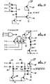
- the logic gate of the invention has multiple wired-AND input circuits 72 and 74, connected to a single power supply +V D through two separate pull-up FET's 76 and 78, respectively.
- input circuit 72 is shown as having inputs A and B wired to it, and input circuit 74 is shown as having inputs C and D.
- Input circuit 72 is also connected to the anode terminal of a diode 80, and input circuit 74 is connected to the anode terminal of another diode 82.
- the cathodes of the two diodes are connected to a junction point 83, and thence through a third diode 84 to the gate of a FET 86, which is also connected through a pull-down FET 88, the source terminal of which is connected to a negative power supply -V s .
- the FET 86 has a single gate terminal, a single source terminal connected to ground, and multiple drain terminals to provide multiple outputs or fanout from the entire circuit.
- the inputs, A and B are derived from output lines like those shown emanating from the multiple drain terminals of FET 86, but supplied, of course, from another copy of the standard logic gate of the invention.
- the inputs A and B are derived from output lines like those shown emanating from the multiple drain terminals of FET 86, but supplied, of course, from another copy of the standard logic gate of the invention.
- there are two inputs A and B coupled to pull-up FET 76 there will be two FET's like the one shown at 86, connected to the input circuit 72. These are shown by way of example at 86' and 86". If either one, or both, of the FET's 86' and 86" are in a conductive state, they act as pull-down FET's, and the voltage on input circuit 72 is pulled down to a low level.
- FET 86 When FET 86 is off, its active outputs are at a positive voltage level, as a result of the pull-up action of FET 76', but when FET 86 is turned on, the voltages at its outputs are pulled down to a near-zero level.
- the FET 86 operates in what is known as the depletion mode.
- a FET becomes conductive, and current flows between its source and drain terminals when the gate-source voltage is raised above a predetermined threshold level.
- the threshold level is below zero. The FET is therefore conductive when the gate-source voltage is zero, and is non-conductive when the gate-source voltage is at a negative value below the threshold.
- Fig. 2 shows the logic-diagram equivalent of the circuit of the invention. It includes two AND gates 90 and one OR gate 92 ' with multiple inverted outputs. The function of the OR gate 92 is performed at the junction 83 (Fig. 1) between diodes 80,82 and 84. As has been described, so long as there are no conductive FET's connected to input 72, there is conduction through FET 88, and the output FET 86 is also turned on. Similarly, if there are no conductive FET's corresponding to the inputs C and D on line 74, there will be current conduction through diodes 82 and 84, and FET86 will be turned on.
- an "on” output condition will result if either A and B are both off, or C and D or both off.
- the "off” condition is one in which there is a positive voltage present. Using a positive logic convention, a positive voltage is equivalent to logic-1 and a zero voltage is equivalent to logic-0. Therefore, “off” is logic-1 and “on” is logic-0, and the logic equation for the circuit is: where F N is the output, the symbols ".” and "+” have their usual meaning of AND and OR, respectively, and the overlining indicates inversion.
- the diodes 80, 82 and 84 perform the ORing function at the junction 83 and a level-shifting function to facilitate use of the output FET 86. It will be understood, however, that the diodes may not be needed if an enhancement-mode FET is employed at the output, and no level-shifting is required.
- Fig. 3 shows how multiple logic gates of the invention can be interconnected.
- the gates U1U5 are each equivalent to the circuitry of Fig. 1.
- Gate U1 has two outputs on lines 96 and 98 coupled as inputs to gates U4 and U3, respectively.
- Gate U2 has two outputs 100 and 102 coupled to gates U3 and U5, respectively.
- the lines 98 and 100 are wire-ANDed for input to gate U3. If, for example, the outputs of U1 are logic-1 and the outputs of U2 are logic-0, the result of the wired-AND operation at the input of gate U3 will be a logic-0 signal.
- Fig. 4 shows how the multiple-drain FET 86 can be fabricated as multiple FET's with gates connected in common to a single gate terminal, and sources connected to a common ground.
- Other specific structures may, of course be used to perform an equivalent function, depending largely on the fabrication process employed.
- the topology of the invention can be compared with other standard FET topologies for identical circuit applications.
- a four-bit adder has been simulated for buffered FET logic (BFL) and differential current-mode logic (DCML), as well as for the wired-AND FET logic (WAFL) of the invention.
- BFL buffered FET logic
- DCML differential current-mode logic
- WAFL wired-AND FET logic
- WAFL has a substantial advantage in propagation delay-power product over the other topologies, and has a substantial advantage also in terms of parts counts. Although the propagation delay for WAFL is greater than that of the DCML version, there is an almost five-fold power advantage over DCML.
- the present invention represents a significant advance in the field of integrated circuitry using FETtechnology.
- the invention provides a basic logic gate that can be conveniently expanded and interconnected through the multiple inputs and outputs it provides.
- the logic gate of the invention has a significant delay-power product advantage over other approaches for the same general purpose.
Landscapes
- Engineering & Computer Science (AREA)
- Physics & Mathematics (AREA)
- Computer Hardware Design (AREA)
- Computing Systems (AREA)
- General Engineering & Computer Science (AREA)
- Mathematical Physics (AREA)
- Power Engineering (AREA)
- Logic Circuits (AREA)
Claims (5)
Applications Claiming Priority (2)
| Application Number | Priority Date | Filing Date | Title |
|---|---|---|---|
| US663004 | 1984-10-19 | ||
| US06/663,004 US4680484A (en) | 1984-10-19 | 1984-10-19 | Wired-AND FET logic gate |
Publications (2)
| Publication Number | Publication Date |
|---|---|
| EP0186940A1 EP0186940A1 (fr) | 1986-07-09 |
| EP0186940B1 true EP0186940B1 (fr) | 1990-09-05 |
Family
ID=24660109
Family Applications (1)
| Application Number | Title | Priority Date | Filing Date |
|---|---|---|---|
| EP85307223A Expired EP0186940B1 (fr) | 1984-10-19 | 1985-10-09 | Porte logique avec ET câblée pour étage d'entrée utilisant des transistors à effet de champ |
Country Status (4)
| Country | Link |
|---|---|
| US (1) | US4680484A (fr) |
| EP (1) | EP0186940B1 (fr) |
| JP (1) | JPS61179616A (fr) |
| DE (1) | DE3579573D1 (fr) |
Families Citing this family (11)
| Publication number | Priority date | Publication date | Assignee | Title |
|---|---|---|---|---|
| US4798979A (en) * | 1986-09-23 | 1989-01-17 | Honeywell Inc. | Schottky diode logic for E-mode FET/D-mode FET VLSI circuits |
| US4965863A (en) * | 1987-10-02 | 1990-10-23 | Cray Computer Corporation | Gallium arsenide depletion made MESFIT logic cell |
| FR2653277A1 (fr) * | 1989-10-17 | 1991-04-19 | Thomson Composants Microondes | Circuit integre logique, a temps de basculement reglable. |
| JP3956347B2 (ja) * | 2002-02-26 | 2007-08-08 | インターナショナル・ビジネス・マシーンズ・コーポレーション | ディスプレイ装置 |
| US10141930B2 (en) * | 2013-06-04 | 2018-11-27 | Nvidia Corporation | Three state latch |
| RU2715178C1 (ru) * | 2019-11-06 | 2020-02-25 | Федеральное государственное бюджетное образовательное учреждение высшего образования "Юго-Западный государственный университет" (ЮЗГУ) | Триггерный логический элемент И на полевых транзисторах |
| RU2756096C1 (ru) * | 2020-12-16 | 2021-09-28 | Федеральное государственное бюджетное образовательное учреждение высшего образования «Юго-Западный государственный университет» (ЮЗГУ) | Триггерный логический элемент и-не/или-не на полевых транзисторах |
| RU2759863C1 (ru) * | 2021-04-28 | 2021-11-18 | Федеральное государственное бюджетное образовательное учреждение высшего образования «Юго-Западный государственный университет» | Триггерный логический элемент И/ИЛИ на полевых транзисторах |
| RU2763585C1 (ru) * | 2021-05-27 | 2021-12-30 | Федеральное государственное бюджетное образовательное учреждение высшего образования «Юго-Западный государственный университет» (ЮЗГУ) (RU) | Триггерный логический элемент И/И-НЕ на полевых транзисторах |
| RU2763152C1 (ru) * | 2021-05-27 | 2021-12-27 | Федеральное государственное бюджетное образовательное учреждение высшего образования «Юго-Западный государственный университет» | Триггерный логический элемент НЕ/ИЛИ/И/ИЛИ-НЕ/И-НЕ на полевых транзисторах |
| US12028059B2 (en) | 2022-03-17 | 2024-07-02 | Raytheon Company | Common gate input circuit for III/V D-mode buffered FET logic (BFL) |
Family Cites Families (9)
| Publication number | Priority date | Publication date | Assignee | Title |
|---|---|---|---|---|
| JPS53108290A (en) * | 1977-03-03 | 1978-09-20 | Seiko Instr & Electronics Ltd | Static induction transistor logic |
| FR2411512A1 (fr) * | 1977-12-06 | 1979-07-06 | Lardy Jean Louis | Porte logique a transistor mos multidrain |
| US4300064A (en) * | 1979-02-12 | 1981-11-10 | Rockwell International Corporation | Schottky diode FET logic integrated circuit |
| FR2457605A2 (fr) * | 1979-05-21 | 1980-12-19 | France Etat | Perfectionnements aux portes logiques a transistors mos multidrains |
| US4418291A (en) * | 1980-05-28 | 1983-11-29 | Raytheon Company | Logic gate having an isolation FET and noise immunity circuit |
| FR2485832A1 (fr) * | 1980-06-24 | 1981-12-31 | Thomson Csf | Inverseur logique, et operateur a plusieurs sorties derive de cet inverseur, utilisant au moins un transistor a effet de champ a faible tension de seuil |
| US4405870A (en) * | 1980-12-10 | 1983-09-20 | Rockwell International Corporation | Schottky diode-diode field effect transistor logic |
| US4423339A (en) * | 1981-02-23 | 1983-12-27 | Motorola, Inc. | Majority logic gate |
| US4404480A (en) * | 1982-02-01 | 1983-09-13 | Sperry Corporation | High speed-low power gallium arsenide basic logic circuit |
-
1984
- 1984-10-19 US US06/663,004 patent/US4680484A/en not_active Expired - Lifetime
-
1985
- 1985-10-09 DE DE8585307223T patent/DE3579573D1/de not_active Expired - Fee Related
- 1985-10-09 EP EP85307223A patent/EP0186940B1/fr not_active Expired
- 1985-10-18 JP JP60233146A patent/JPS61179616A/ja active Pending
Also Published As
| Publication number | Publication date |
|---|---|
| DE3579573D1 (de) | 1990-10-11 |
| US4680484A (en) | 1987-07-14 |
| JPS61179616A (ja) | 1986-08-12 |
| EP0186940A1 (fr) | 1986-07-09 |
Similar Documents
| Publication | Publication Date | Title |
|---|---|---|
| US5656948A (en) | Null convention threshold gate | |
| US4486670A (en) | Monolithic CMOS low power digital level shifter | |
| US4710649A (en) | Transmission-gate structured logic circuits | |
| US4831285A (en) | Self precharging static programmable logic array | |
| EP0085569A2 (fr) | Circuit logique à l'arséniure de gallium | |
| US5664211A (en) | Null convention threshold gate | |
| US5097148A (en) | Integrated circuit buffer with improved drive capability | |
| JPH035692B2 (fr) | ||
| US4680484A (en) | Wired-AND FET logic gate | |
| US4749886A (en) | Reduced parallel EXCLUSIVE or and EXCLUSIVE NOR gate | |
| US6900658B1 (en) | Null convention threshold gate | |
| US5155387A (en) | Circuit suitable for differential multiplexers and logic gates utilizing bipolar and field-effect transistors | |
| US4490632A (en) | Noninverting amplifier circuit for one propagation delay complex logic gates | |
| US4943740A (en) | Ultra fast logic | |
| US4395645A (en) | Mosfet logic inverter buffer circuit for integrated circuits | |
| US5027007A (en) | FFL/QFL FET logic circuits | |
| US4767950A (en) | MOS inverter circuit having two different supply voltages | |
| US6437602B1 (en) | Fully dynamic logic network circuits | |
| US4716311A (en) | Direct coupled FET logic with super buffer output stage | |
| Hoe et al. | Dynamic GaAs capacitively coupled domino logic (CCDL) | |
| EP0380095B1 (fr) | Circuit logique | |
| EP0356108A2 (fr) | Porte logique à effet de champ source-suiveur (SFFL) réalisable en technologies III-V | |
| US5661411A (en) | Feedback controlled load logic circuit | |
| US3582683A (en) | Optionally clocked transistor circuits | |
| US4704544A (en) | Complementary current mirror logic |
Legal Events
| Date | Code | Title | Description |
|---|---|---|---|
| PUAI | Public reference made under article 153(3) epc to a published international application that has entered the european phase |
Free format text: ORIGINAL CODE: 0009012 |
|
| AK | Designated contracting states |
Kind code of ref document: A1 Designated state(s): DE FR GB IT NL |
|
| 17P | Request for examination filed |
Effective date: 19861211 |
|
| 17Q | First examination report despatched |
Effective date: 19881212 |
|
| ITF | It: translation for a ep patent filed | ||
| GRAA | (expected) grant |
Free format text: ORIGINAL CODE: 0009210 |
|
| AK | Designated contracting states |
Kind code of ref document: B1 Designated state(s): DE FR GB IT NL |
|
| REF | Corresponds to: |
Ref document number: 3579573 Country of ref document: DE Date of ref document: 19901011 |
|
| ET | Fr: translation filed | ||
| PLBE | No opposition filed within time limit |
Free format text: ORIGINAL CODE: 0009261 |
|
| STAA | Information on the status of an ep patent application or granted ep patent |
Free format text: STATUS: NO OPPOSITION FILED WITHIN TIME LIMIT |
|
| 26N | No opposition filed | ||
| ITTA | It: last paid annual fee | ||
| PGFP | Annual fee paid to national office [announced via postgrant information from national office to epo] |
Ref country code: NL Payment date: 19980914 Year of fee payment: 14 |
|
| PGFP | Annual fee paid to national office [announced via postgrant information from national office to epo] |
Ref country code: GB Payment date: 19981001 Year of fee payment: 14 |
|
| PGFP | Annual fee paid to national office [announced via postgrant information from national office to epo] |
Ref country code: FR Payment date: 19981006 Year of fee payment: 14 |
|
| PGFP | Annual fee paid to national office [announced via postgrant information from national office to epo] |
Ref country code: DE Payment date: 19981028 Year of fee payment: 14 |
|
| PG25 | Lapsed in a contracting state [announced via postgrant information from national office to epo] |
Ref country code: GB Free format text: LAPSE BECAUSE OF NON-PAYMENT OF DUE FEES Effective date: 19991009 |
|
| PG25 | Lapsed in a contracting state [announced via postgrant information from national office to epo] |
Ref country code: NL Free format text: LAPSE BECAUSE OF NON-PAYMENT OF DUE FEES Effective date: 20000501 |
|
| GBPC | Gb: european patent ceased through non-payment of renewal fee |
Effective date: 19991009 |
|
| PG25 | Lapsed in a contracting state [announced via postgrant information from national office to epo] |
Ref country code: FR Free format text: LAPSE BECAUSE OF NON-PAYMENT OF DUE FEES Effective date: 20000630 |
|
| NLV4 | Nl: lapsed or anulled due to non-payment of the annual fee |
Effective date: 20000501 |
|
| PG25 | Lapsed in a contracting state [announced via postgrant information from national office to epo] |
Ref country code: DE Free format text: LAPSE BECAUSE OF NON-PAYMENT OF DUE FEES Effective date: 20000801 |
|
| REG | Reference to a national code |
Ref country code: FR Ref legal event code: ST |