EP0186974A2 - Circuit intégré pour vérifier des limites - Google Patents
Circuit intégré pour vérifier des limites Download PDFInfo
- Publication number
- EP0186974A2 EP0186974A2 EP85308673A EP85308673A EP0186974A2 EP 0186974 A2 EP0186974 A2 EP 0186974A2 EP 85308673 A EP85308673 A EP 85308673A EP 85308673 A EP85308673 A EP 85308673A EP 0186974 A2 EP0186974 A2 EP 0186974A2
- Authority
- EP
- European Patent Office
- Prior art keywords
- data
- signal
- low
- word
- compared
- Prior art date
- Legal status (The legal status is an assumption and is not a legal conclusion. Google has not performed a legal analysis and makes no representation as to the accuracy of the status listed.)
- Granted
Links
Images


Classifications
-
- G—PHYSICS
- G06—COMPUTING OR CALCULATING; COUNTING
- G06F—ELECTRIC DIGITAL DATA PROCESSING
- G06F7/00—Methods or arrangements for processing data by operating upon the order or content of the data handled
- G06F7/02—Comparing digital values
- G06F7/026—Magnitude comparison, i.e. determining the relative order of operands based on their numerical value, e.g. window comparator
Definitions
- This invention relates generally to digital integrated circuitry which compares 16-bit data values against lower and upper limits and, more particularly, to a single-chip circuit which can compare numbers selectively in an unsigned mode or a signed two's complement mode without loss of speed relative to a device which operates exclusively on unsigned or exclusively on signed numbers.
- a computer may utilize a virtual memory in which a selectable contiguous part of the virtual memory is mapped into random access memory (RAM) prcviding relatively faster read/write access times.
- RAM random access memory
- Most of the instructions executed on the computer address locations within the fast RAM, however certain relatively-infrequent instructions such as load and store may address any location within the virtual memory.
- apparatus is needed which can operate in real time to detect numeric values, here addresses, which fall outside a pair of numeric boundaries.
- the prior art has constructed such bounds checker apparatus with discrete medium-scale integrated circuit (MSI) devices; in one instance, a 16-bit checker consisting of four 8-bit registers and four 8-bit comparators.
- MSI medium-scale integrated circuit
- a single-chip 16-bit bounds checker embodying the present invention can be produced at one-third the cost of the prior art discrete component approach, using one-eighth of board space of the space used in the prior art approach.
- the single-chip bounds checker requires only one-tenth the power of the prior art bounds checkers and affects a 20 percent improvement in cycle times. Interconnection of the more than 100 pins used in the discrete approach of the prior art is considerably reduced since the single-chip bounds checker requires only 28 pins.
- the single-chip bounds checker can be operated in either an unsigned mode capable of processing data in the range 0 to 2 16- 1 or ina signed mode capable of processing data in the range -2 15 to +2 -1.
- the mode is selected by a signal applied to a terminal pin of the bounds checker.
- a shared sixteen-bit wide input data bus receives the lower and upper limit values which are then loaded into lower and upper limit on-chip registers upon receipt of load lower and load upper signals. Data values to be compared against these limits are also presented on the shared input data bus.
- a novel feature of the bounds checker provides the testing of either unsigned or signed two's complement numbers as described without imposing additional delay over a bounds checker which can operate only on one type of number.
- three outputs are provided for presenting the results of testing a data value against the programmable lower and upper limits.
- a signal is a HIGH if the data value exceeds (or equals) the lower limit
- a second output is a HIGH if the data value is less than (or equals) the upper limit
- at a third output a signal is a LOW if the data value is strictly between (or not outside) the lower and the upper limit.
- the choice of whether the tests will include or net. include the parenthesized portion of the tests just described is selectable by the application of suitable signals to certain of the terminal pins of the bounds checker.
- the bounds checker is readily cascaded to provide a bounds checker capable of testing extended- precision values.
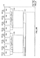
- the bounds checker 10 receives 16-bit data words at a set of sixteen data input terminals DATA_IN 0-15 .
- the data input terminals are connected via a 16-bit data bus 20 to a lower bound register 22, an upper bound register 24, a lower comparator 26 and an upper comparator 28.
- the 16-bit data bus 20 is shared by the registers 22 and 24 and the comparators 26 and 28 so that the signals representing the 16-bit number- to-be-compared and the 16-bit numbers forming the lower and upper comparison limits can be placed onto the data input terminals of bounds checker 10 and conducted to the appropriate element therein.
- the lower bound register 22 receives on signal line 30 a load lower bound register signal applied to a load lower (LOAD LOWER) terminal of bounds checker 10.
- a 16-bit signal a pplied to the DATA_IN 0-15 terminals of bounds checker 10 is conducted via bus 20 to an inverted input of lower bound register 22 and upon application of the load lower bound register signal, the 16-bit complemented signals are received and stored in register 22.
- Lower bound register 22 also receives a clock pulse applied to a clock (CLK) terminal of bounds checker 10 and conducted to register 22 via signal line 22.
- CLK clock
- the 17-bit output of lower bound register 22 consists of the (complemented) value of each of the lower-order fifteen bit complemented signals received and stored within register 22, plus the true and complemented value of the most-significant bit (msb) signal received and stored therein.
- the seventeen output signals are conducted via bus 34 to lower comparator 26.
- the upper bound register 24 receives on a signal line 36 a load upper bound register signal applied to a load upper (LOAD UPPER) terminal of the bounds checker 10.
- a 16-bit si g nal applied to the DATA_IN 0-15 terminals of checker 10 is conducted (in true values) as described above in connection with register 22.
- the 17-bit output signals of upper bound register 24 the true value of each of the lower-order bits, plus the true and complemented value of the msb is conducted via a bus 38 to upper comparator 28.
- lower comparator 26 receives a 17-bit signal comprising the 16-bit true signals on the data bus 20 and the one-bit complemented signal of the msb on the data bus 20.
- upper comparator 28 receives at an inverted input the 16-bit signal on the data bus 20 and the one-bit true signal of the msb on the data bus 20.
- the lower comparator 26 also receives a carry-zero-low (C 0,L ) signal applied to a CARRY IN LOWER terminal of the bounds checker 10 and conducted therefrom via a signal line 40.
- Upper comparator 28 receives a carry-zero-upper (C 0,U ) signal applied to a CARRY_IN_UPPER terminal of the bounds checker 10 and conducted therefrom via signal line 42.
- Comparators 26 and 28 also receive a signed-mode signal applied to a SIGNED terminal of the bounds checker 10 and conducted therefrom via a signal line 44.
- Lower comparator 26 generates on signal line 46 a complement carry-sixteen-lower (C 16 , L ) signal conducted via an inverter 47 to a LOWER OUT terminal of bounds checker 10 and conducted to a first complemented input of an AND gate 50.
- Upper comparator 28 generates on signal line 48 a complement carry-sixteen-upper (C 16 , U ) signal conducted via an inverter 49 to an U P -PER OUT terminal of bounds checker 10 and conducted to a second input of the AND gate 50.
- the inverted output of AND gate 50 is connected to an OUT_OF_BOUNDS output terminal of bounds checker 10.
- the signals C 16 , L and C 16 , U generated at the outputs of the comparators 26 and 28, respectively are related to the C O , L and C 0,U signals applied to the CARRY_IN_LOWER and CARRY_IN_UPPER terminals respectively, in accordance with Table I, below.
- the entries in the column labelled LOWER OUT refer to the conditions which must prevail between the current contents of the lower bound register 22, denoted “L” in Table I, and the current value applied to the DATA_IN 0-15 terminals, denoted “D” in Table I, to cause a LOW C 16 , L signal to be generated by lower comparator 26, and accordingly a HIGH C 16 , L signal to be received at the LOWER OUT terminal of bounds checker 10.
- the lower comparator 26 generates a LOW C 16 , L signal if and only if the current contents in the lower bound register 22 is strictly less than the current value applied to the DATA_IN 0-15 terminals.
- the signal at the OUT_OF_BOUNDS output of bounds checker 10 is related to the signals -C 16,L and C 16 , U according to the equation: and therefore represents the failure of either (or both) conditions which cause a HIGH signal at the LOWER_OUT or the UPPER OUT terminals to be received, in accordance with Table I, above, as determined by the signals at the CARRY IN LOWER and the CARRY IN UPPER terminals.
- the bounds checker 10 can be selectively operated in either a signed (two's complement) mode or an unsigned mode depending on whether a HIGH, or a LOW, respectively signal is applied to the SIGNED terminal of the bounds checker.
- the lower and upper limit and data numbers are treated as signed 16- bit, or unsigned 16-bit integers, respectively, and the comparisons are affected in accordance with Table I, above, as determined by the signals at the CARRY_IN_LOWER and the CARRY IN UPPER terminals.
- the bounds checker 10 implements the ability to operate on both signed and unsigned numbers in a way that extracts no additional time penalty in the cycle time of the device.
- the value 2 15 is added to all the numbers, lower and upper limits and data, to be used in the comparison operation under control of the signal applied to the SIGNED terminal and conducted via signal line 44 to the comparators 26 and 28.
- the addition is accomplished by complementing the most significant bit, i.e. bit position 15, of the signals received at the comparators 26 and 28 by the propagate and generate circuits of a carry lookahead logic circuit interior to the comparators 26 and 28 in a way that does not add to the combinatorial delay of the circuit.
- Fig. 2 illustrates the circuitry internal to the lower comparator 26 of the bounds checker 10, (and typical of the circuitry internal to the upper comparator 28).
- the signals applied to the DATA_IN 0-15 terminal of the bounds checker 10 are conducted to comparator 26 together with the complement of the signal applied to the DATA_IN 15 terminal.
- the 15 complemented signals generated by the lower bound register 22, Q i,L , i 14, 13, ..., 1, 0; are conducted to a second input of the respective one of the set of fifteen logic circuits 100a, 100b, ..., 100 0 ; i.e., logic circuit 100a receives the signal Q 14;L " logic circuit 100o receives the signal Q 0,L .
- Logic circuit 100a typical of the remaining logic circuits 100b, ..., 100o, includes a NAND gate 102a and a NOR gate 104a which each receive at a first input the signal conducted from the DATA-IN14 terminal and at a second input the Q 14,L signal. Because the complement of the signal representing the contents of the lower bound register 22, is applied to the logic circuits 100a, 100b, ..., 100o along with the true signal conducted from the DATA_IN 0-14 terminals, the logic circuits perform. a subtraction of the low-order fifteen bits of the lower bound from the data-value-to-be-compared through one's complement addition.
- the signals at the output of the NAND gate 107a and of the NOR gate 104a of logic circuit 100a represent the complement of a generate and propagate signal, respectively, which is conducted to a four-bit lookahead carry circuit 106a, typical of lookahead carry circuits 106b, 106c and 106d.
- the corresponding complemented generate and propagate signals generated by the logic circuits 100b and 100c are likewise conducted to lookahead carry logic circuit 106a.
- the generate and propagate signals generated by the four logic circuits 100d, ..., 100g, the four logic circuits 100h, ..., 100k, the four logic circuits 1001, ..., 100o are conducted to lookahead carry circuits 106b, 106c and 106d, respectively.
- Generate and propagate signals generated by the four first-level carry circuits 106a, ..., 106d are conducted to a second-level lookahead carry circuit 108 which also receives the carry-zero-low (C O,L ) signal via the signal line 40.
- the circuitry internal to the lookahead carry circuits 106a, ..., 106d and 108 is conventional and the circuits function in a manner well known to those skilled in the art.
- the operation of the above-described elements of the comparator 26 illustrated in Fig. 2 is conventional, and as mentioned, performs a one's complement addition of the low-order fifteen bits of the data-value-to-be-compared (DO -14 ) and the low-order fifteen bits of the contents of the lower bound register 22 (L 0-14 ).
- the generate and propagate signals generated within the second-level lookahead carry circuit 108 are wired-OR together to form the C 16 , L signal generated at the output of the circuit 108 and conducted via signal line 46 and inverter 47 to the LOWER OUT terminal of the bounds checker 10.
- the carry-out signal C 16 , L is a HIGH if either a final generate signal or a final propagate signal (or both) was generated as a result of the one's complement addition of the low-order 15 bits D 0-14 and L 0-14' as shown in Table II below.
- the carry-out signal C 16 , L is a LOW if neither the final generate signal, nor the final propagate signal was generated, i.e., the signal at the LOWER OUT terminal is a HIGH if and only if the resulting subtraction produces neither a generate signal nor a propagate signal.
- the first row of Table II corresponds to the situation where a LOW carry-in signal is applied to the lower comparator 26.
- the resulting carry-out signal C 16,L generated by the second-level lookahead carry logic circuit 108 of comparator 26 is the carry resulting from a one's complement addition (i.e., subtraction) of the subtrahend L 0-14 and the D 0-14 values. Due to the characteristics of one's complement arithmetic the resulting value is, as shown, D 0-14 - L 0-14 -1.
- the bounds checker 10 can process signed as well as unsigned lower and upper limits and data-to-be-compared values.
- Unsigned 16-bit values in the range 0 to 2 16 - 1 are treated as described above by the comparators 26 (and 28) in that the low-order fifteen bits of the lower limit, L 0-14 , are subtracted from the data-value-to-be-compared, D 0-14 , as described and the true and complemented signals corresponding to the most-significant bits L15 and D15 of the lower limit and the data-value-to-be-compared, respectively, are conducted from the lower bound register 22 and the DATA_IN 15 terminal of bounds checker 10, respectively, to a special logic circuit 110, within lower comparator 26.
- Special logic circuit 110 includes a pair of OR gates 112 and 114 which each receive at a first input the signal conducted from the most-significant DATA_IN 15 terminal of the bounds checker 10 and at a second input the most-significant Q 15,L signal generated by the lower bound register 22.
- Circuit 110 also includes a pair of OR gates 116 and 118 which each receive at a first input the complemented signal conducted from the DATA_IN 15 terminal, and at a second input the most-significant Q 15 , L signal generated by the lower bound register 22.
- Special logic circuit 110 also includes a pair of 2:1 multiplexers (2:1 MUX) 120 and 122 which each receive the signed-mode signal conducted on signal line 44 from the SIGNED terminal of bounds checker 10.
- Multiplexer 120 is connected to the outputs of the OR gates 112 and 116 and under control of the signed-mode signal conducts either the signal at the output of OR gate 112, or OR gate 116, to an output of the multiplexer 120, depending on whether the signed-mode signal is a HIGH, or a LOW, respectively.
- Multiplexer 122 is connected to the outputs of the OR gates 114 and 118 and under control of the signal-mode signal conducts either the signal at the output of OR gate 114, or OR gate 118, to an inverting output of the multiplexer 122, depending on whether the signed-mode signal is a LOW, or a HIGH, respectively.
- the output of multiplexer 120 is connected to the most-significant inverted generate input of carry lookahead circuit 106a and the inverted output of multiplexer 122 is connected to the most-significant inverted propagate input of carry lookahead circuit 106a.
- a LOW is applied to the SIGNED terminal and a LOW signed-mode signal is conducted to the 2:1 MUX 120 and the 2:1 MUX 122 which causes the logical "OR" signal composed from the signals on the complemented DATA_IN 15 and the Q 15 , L input to the OR gate 116 and the logical "OR” signal composed from the signals on the DATA_IN 15 and the Q 15,L input to the OR gate 114 to be conducted to the most-significant generate and propagate respectively, inputs of lookahead carry circuit 106a.
- the special half-adder circuit 110 generates generate and propagate signals from the most-significant bits of the lower limit L 15 and the data-value-to-be-compared D15 in the same manner, and with no more gate delay than, as for the lower-order fifteen bits, as previously described; i.e., i.e., the NAND operation applied to the true signal applied to the DATA_IN 15 terminal and to complement of the Q 15,L signal, and the NOR operation applied to the same signals.
- a HIGH signal is applied to the SIGNED terminal and a HIGH signed-mode signal is conducted to the 2:1 MUX 120 and 122, which causes the logical "OR" signal composed from the signals on the true DATA_IN 15 and the Q15,L input to the OR gate 112 and the logical "OR” signal composed from the signals on the complemented DATA_IN 15 and the Q 15 , L input to the OR gate 118 to be conducted to the most-significant inverted generate and inverted propagate inputs, respectively, of lookahead carry logic circuit 106a.
- the complements of the signals used to generate the most-significant inverted generate and inverted propagate signals for input to circuit 106a during the unsigned mode are used to generate these inverted generate and propagate signals, i.e., Accordingly, during the signed mode the lower comparator 22 operates on values which are complemented in their most-significant bits for the lower limit value and the data-value-to-be-compared, with no additional gate delay when carrying out the comparison.
- the bounds checker 10 is designed to operate on two's complement signed numbers in the range from - 2 15 to 2 15 - 1 representing the upper and lower limits and the data-value-to-be-compared and hence the above-described complementation effectively adds 2 15 to all values to be compared during the signed mode. This addition in no way affects the outcome of the comparisons but shifts the range of signed numbers into the range 0 to 2 16 - 1 , i.e. identical with the range of unsigned numbers which can then be compared exactly as described before for unsigned numbers, in a way which imposes no combinatorial delay regardless of the mode in which the bounds checker 10 is operated.
- the internal circuitry and operation of the upper comparator 28 effects the comparison by a subtraction of the data-value-to-be-compared from the contents of the upper bound register 24 in a manner entirely analogous to that just described for the lower comparator 26 and therefore no further explanation will be supplied herein.
- the bounds checker 10 can be connected with other bounds checkers 10 to provide an extended precision bounds checker.
- Fig. 3 illustrates the interconnection of two bounds checkers 10 to form a 32-bit bounds checker.
- one bounds checker 10 (“low-order checker”) receives the low-order sixteen bits of the lower limit, upper limit and data-value-to-be-compared at its DATA_IN 0-15 terminals.
- the upper-order sixteen bits of these numbers are received at a second bounds checker 10 ("high-order checker”) relabel- led DATA_IN 16-31 terminals.
- the LOAD LOWER, LOAD UPPER and CLK terminals of both bounds checkers 10 are connected in parallel.
- the LOWER_OUT and UPPER OUT terminals of the low-order checker 10 are connected to the CARRY_IN_LOWER and the CARRY_IN_UPPER terminals, respectively, of the upper-order checker 10.
- the SIGNED terminal of the lower-order checker 10 is tied to a LOW signal, and the CARRY IN LOWER and CARRY_IN_UPPER terminals thereof receive the C 0,L and C 0,U signals, respectively, of the 32-bit checker.
- the SIGNED terminal of the upper-order checker 310 receives the signed-mode signal of the 32-bit checker, and the LOWER OUT, OUT_OF_BOUNDS and, UPPER_OUT terminals thereof form the output terminals of the 32-bit checker.
- the parallel connection of the clock and the LOAD LOWER and LOAD UPPER terminals afford simultaneous loading of the lower order and upper order 16-bit portions of the 32-bit lower and upper limit values, into the respective low-order and high-order bounds checker. Tying the SIGNED terminal of the low-order bounds checker 10 to a LOW causes the special logic circuit 110 therein to affect a normal (unsigned) comparison of the lower-order portions of the lower and upper limit values against the lower-order portion of the data-value-to-be-compared.
- Application of the appropriate signed-mode signal to the SIGNED terminal of the high-order bounds checker 10 causes the special logic circuit 110 therein to affect either an unsigned or signed comparison by either using the normal or the complemented values of the most-significant, i.e. 31st, bits of the lower and upper limits and the data-value-to-be-compared during the subtractions performed by the comparators 26 and 28 within the upper-order bounds checker.
- the C 16 , L and C 16 , U carry-out signals generated by the low-order bounds checker 10 are applied as the C O , L and C O,U , carry-in signals, respectively, to the high-order bounds checker and therefore the lower-order and high-order carry-out signals generated by the second level carry lookahead circuits of the comparators 26 and 28 within the high-order bounds checker will be correctly adjusted for any potential carries out of the low-order bounds checker 10. Accordingly, the outputs of the high-order bounds checker, LOWER OUT, OUT OF BOUNDS and UPPER OUT will reflect the correct result of the comparisons with the 32-bit upper and lower limit values against the 32-bit data-value-to-be-compared.
Landscapes
- Physics & Mathematics (AREA)
- General Physics & Mathematics (AREA)
- Engineering & Computer Science (AREA)
- Theoretical Computer Science (AREA)
- Computational Mathematics (AREA)
- Mathematical Analysis (AREA)
- Mathematical Optimization (AREA)
- Pure & Applied Mathematics (AREA)
- General Engineering & Computer Science (AREA)
- Tests Of Electronic Circuits (AREA)
- Test And Diagnosis Of Digital Computers (AREA)
- Techniques For Improving Reliability Of Storages (AREA)
Priority Applications (1)
| Application Number | Priority Date | Filing Date | Title |
|---|---|---|---|
| AT85308673T ATE90161T1 (de) | 1984-11-29 | 1985-11-28 | Integrierte schaltung fuer grenzwertpruefung. |
Applications Claiming Priority (2)
| Application Number | Priority Date | Filing Date | Title |
|---|---|---|---|
| US676362 | 1984-11-29 | ||
| US06/676,362 US4760374A (en) | 1984-11-29 | 1984-11-29 | Bounds checker |
Publications (3)
| Publication Number | Publication Date |
|---|---|
| EP0186974A2 true EP0186974A2 (fr) | 1986-07-09 |
| EP0186974A3 EP0186974A3 (en) | 1989-05-31 |
| EP0186974B1 EP0186974B1 (fr) | 1993-06-02 |
Family
ID=24714204
Family Applications (1)
| Application Number | Title | Priority Date | Filing Date |
|---|---|---|---|
| EP85308673A Expired - Lifetime EP0186974B1 (fr) | 1984-11-29 | 1985-11-28 | Circuit intégré pour vérifier des limites |
Country Status (5)
| Country | Link |
|---|---|
| US (1) | US4760374A (fr) |
| EP (1) | EP0186974B1 (fr) |
| JP (1) | JPS61131036A (fr) |
| AT (1) | ATE90161T1 (fr) |
| DE (1) | DE3587383T2 (fr) |
Cited By (3)
| Publication number | Priority date | Publication date | Assignee | Title |
|---|---|---|---|---|
| US4857882A (en) * | 1985-07-02 | 1989-08-15 | Vlsi Technology, Inc. | Comparator array logic |
| US5624661A (en) * | 1990-04-10 | 1997-04-29 | Unger; Evan C. | Hypoosmotic compositions comprising a polymer and a complexed contrast agent for MRI |
| FR2776787A1 (fr) * | 1998-03-31 | 1999-10-01 | Sgs Thomson Microelectronics | Comparateur numerique |
Families Citing this family (25)
| Publication number | Priority date | Publication date | Assignee | Title |
|---|---|---|---|---|
| CA1264072A (fr) * | 1986-12-23 | 1989-12-27 | Robert J. Inkol | Filtre de parametres reconfigurable |
| AU606559B2 (en) * | 1987-12-24 | 1991-02-07 | Nec Corporation | Circuit for comparing a plurality of binary inputs |
| US5023590A (en) * | 1989-12-06 | 1991-06-11 | Loral Aerospace Corp. | 17-bit cascadable comparator using generic array logic |
| US5172091A (en) * | 1991-04-01 | 1992-12-15 | Arnold Jeffrey W | Asynchronous parallel status comparator |
| DE4129423A1 (de) * | 1991-09-04 | 1993-03-11 | Siemens Ag | Digitale logikschaltung zur realisierung unscharfer (fuzzy logic) operatoren |
| US5257216A (en) * | 1992-06-10 | 1993-10-26 | Intel Corporation | Floating point safe instruction recognition apparatus |
| US5469376A (en) * | 1993-10-14 | 1995-11-21 | Abdallah; Mohammad A. F. F. | Digital circuit for the evaluation of mathematical expressions |
| JPH09293066A (ja) * | 1996-04-26 | 1997-11-11 | Wacom Co Ltd | ベクトル演算装置およびベクトル演算方法 |
| US6081820A (en) * | 1998-02-20 | 2000-06-27 | Siemens Energy & Automation | Method and apparatus for filtering a signal using a window value |
| US6341296B1 (en) * | 1998-04-28 | 2002-01-22 | Pmc-Sierra, Inc. | Method and apparatus for efficient selection of a boundary value |
| US7133400B1 (en) | 1998-08-07 | 2006-11-07 | Intel Corporation | System and method for filtering data |
| US7333484B2 (en) * | 1998-08-07 | 2008-02-19 | Intel Corporation | Services processor having a packet editing unit |
| US6114946A (en) * | 1998-09-10 | 2000-09-05 | Lsi Logic Corporation | Combinational logic for comparing N-bit wide buses |
| US6721842B2 (en) | 1999-01-29 | 2004-04-13 | Intel Corporation | Boundary addressable memory |
| US6519620B1 (en) * | 1999-04-22 | 2003-02-11 | International Business Machines Corporation | Saturation select apparatus and method therefor |
| US6499046B1 (en) * | 1999-05-20 | 2002-12-24 | International Business Machines Corporation | Saturation detection apparatus and method therefor |
| US6408383B1 (en) * | 2000-05-04 | 2002-06-18 | Sun Microsystems, Inc. | Array access boundary check by executing BNDCHK instruction with comparison specifiers |
| DE10041511C1 (de) * | 2000-08-24 | 2001-08-09 | Infineon Technologies Ag | Additionsschaltung für digitale Daten |
| WO2002043069A2 (fr) * | 2000-11-07 | 2002-05-30 | Fast-Chip, Inc. | Memoire adressable par la limite |
| US7284028B2 (en) * | 2002-11-01 | 2007-10-16 | International Business Machines Corporation | Comparator eliminating need for one's complement logic for signed numbers |
| DE10317651A1 (de) * | 2003-04-17 | 2004-11-04 | Robert Bosch Gmbh | Verfahren und Vorrichtung zum Vergleichen von binären Datenworten |
| US20060095713A1 (en) * | 2004-11-03 | 2006-05-04 | Stexar Corporation | Clip-and-pack instruction for processor |
| US7962729B2 (en) * | 2009-01-05 | 2011-06-14 | International Business Machines Corporation | Dynamic runtime range checking of different types on a register using upper and lower bound value registers for the register |
| US20100185907A1 (en) * | 2009-01-16 | 2010-07-22 | Sun Microsystems, Inc. | Method for bounds testing in software |
| US11347551B2 (en) * | 2019-08-13 | 2022-05-31 | Intel Corporation | Methods, systems, articles of manufacture and apparatus to manage memory allocation |
Family Cites Families (10)
| Publication number | Priority date | Publication date | Assignee | Title |
|---|---|---|---|---|
| US3487364A (en) * | 1966-02-01 | 1969-12-30 | Clare & Co C P | Digital comparator utilizing magnetic logic |
| US3601804A (en) * | 1969-03-14 | 1971-08-24 | British Aircraft Corp Ltd | Digital comparator utilizing dual circuits for self-checking |
| US3757298A (en) * | 1972-08-14 | 1973-09-04 | Bendix Corp | Decimal limit set for a binary digital signal comparison |
| US3845465A (en) * | 1973-01-12 | 1974-10-29 | Us Air Force | Associative storage apparatus for comparing between specified limits |
| US3931612A (en) * | 1974-05-10 | 1976-01-06 | Triad Systems Corporation | Sort apparatus and data processing system |
| US3970833A (en) * | 1975-06-18 | 1976-07-20 | The United States Of America As Represented By The Secretary Of The Navy | High-speed adder |
| US4205302A (en) * | 1977-10-28 | 1980-05-27 | Einar Godo | Word recognizing system |
| US4382179A (en) * | 1980-07-21 | 1983-05-03 | Ncr Corporation | Address range timer/counter |
| US4495565A (en) * | 1981-11-09 | 1985-01-22 | At&T Bell Laboratories | Computer memory address matcher and process |
| US4584666A (en) * | 1984-06-21 | 1986-04-22 | Motorola, Inc. | Method and apparatus for signed and unsigned bounds check |
-
1984
- 1984-11-29 US US06/676,362 patent/US4760374A/en not_active Expired - Lifetime
-
1985
- 1985-11-28 DE DE85308673T patent/DE3587383T2/de not_active Expired - Fee Related
- 1985-11-28 JP JP60269209A patent/JPS61131036A/ja active Pending
- 1985-11-28 EP EP85308673A patent/EP0186974B1/fr not_active Expired - Lifetime
- 1985-11-28 AT AT85308673T patent/ATE90161T1/de not_active IP Right Cessation
Cited By (6)
| Publication number | Priority date | Publication date | Assignee | Title |
|---|---|---|---|---|
| US4857882A (en) * | 1985-07-02 | 1989-08-15 | Vlsi Technology, Inc. | Comparator array logic |
| US5624661A (en) * | 1990-04-10 | 1997-04-29 | Unger; Evan C. | Hypoosmotic compositions comprising a polymer and a complexed contrast agent for MRI |
| US5645816A (en) * | 1990-04-10 | 1997-07-08 | Imarx Pharmaceutical Corp. | Synthetic polyuronic and hypoosmotic polymer compositions in admixture with proteinaceously bound contrast agents for MRI |
| US5658550A (en) * | 1990-04-10 | 1997-08-19 | Imarx Pharmaceutical Corp. | Non cross-linked synthetic polymers as contrast media for magnetic resonance imaging |
| US5681542A (en) * | 1990-04-10 | 1997-10-28 | Imarx Pharmaceutical Corp. | Compositions comprising a biocompatible gas and a polymer for magnetic resonance imaging |
| FR2776787A1 (fr) * | 1998-03-31 | 1999-10-01 | Sgs Thomson Microelectronics | Comparateur numerique |
Also Published As
| Publication number | Publication date |
|---|---|
| EP0186974A3 (en) | 1989-05-31 |
| US4760374A (en) | 1988-07-26 |
| ATE90161T1 (de) | 1993-06-15 |
| JPS61131036A (ja) | 1986-06-18 |
| DE3587383T2 (de) | 1993-12-09 |
| EP0186974B1 (fr) | 1993-06-02 |
| DE3587383D1 (de) | 1993-07-08 |
Similar Documents
| Publication | Publication Date | Title |
|---|---|---|
| US4760374A (en) | Bounds checker | |
| EP0171190B1 (fr) | Unité arithmétique et logique à fonction étendue | |
| US4577282A (en) | Microcomputer system for digital signal processing | |
| US4785421A (en) | Normalizing circuit | |
| US6288570B1 (en) | Logic structure and circuit for fast carry | |
| US4514805A (en) | Interrupt operation in systems emulator mode for microcomputer | |
| US4491910A (en) | Microcomputer having data shift within memory | |
| US4225934A (en) | Multifunctional arithmetic and logic unit in semiconductor integrated circuit | |
| KR920008280B1 (ko) | 집적 프로세서 | |
| US4677586A (en) | Microcomputer device having test mode substituting external RAM for internal RAM | |
| US4498135A (en) | Microcomputer with accumulator addressing | |
| US4422143A (en) | Microprocessor ALU with absolute value function | |
| US4608634A (en) | Microcomputer with offset in store-accumulator operations | |
| US3699326A (en) | Rounding numbers expressed in 2{40 s complement notation | |
| EP0303009A2 (fr) | Générateur de signal d'adressage circulaire | |
| US4503511A (en) | Computing system with multifunctional arithmetic logic unit in single integrated circuit | |
| Lutz et al. | Design of the mosaic element | |
| EP0033346A1 (fr) | Circuit a increment/decrement. | |
| US4783757A (en) | Three input binary adder | |
| US5375081A (en) | High speed adder using a varied carry scheme and related method | |
| US4815019A (en) | Fast ALU equals zero circuit | |
| US4380051A (en) | High speed digital divider having normalizing circuitry | |
| US5126965A (en) | Conditional-sum carry structure compiler | |
| US4506322A (en) | Read/write memory cell for microcomputer | |
| EP0086307B1 (fr) | Système microordinateur pour traitement numerique de signaux |
Legal Events
| Date | Code | Title | Description |
|---|---|---|---|
| PUAI | Public reference made under article 153(3) epc to a published international application that has entered the european phase |
Free format text: ORIGINAL CODE: 0009012 |
|
| AK | Designated contracting states |
Kind code of ref document: A2 Designated state(s): AT BE CH DE FR GB IT LI LU NL SE |
|
| PUAL | Search report despatched |
Free format text: ORIGINAL CODE: 0009013 |
|
| AK | Designated contracting states |
Kind code of ref document: A3 Designated state(s): AT BE CH DE FR GB IT LI LU NL SE |
|
| 17P | Request for examination filed |
Effective date: 19890629 |
|
| 17Q | First examination report despatched |
Effective date: 19910902 |
|
| GRAA | (expected) grant |
Free format text: ORIGINAL CODE: 0009210 |
|
| AK | Designated contracting states |
Kind code of ref document: B1 Designated state(s): AT BE CH DE FR GB IT LI LU NL SE |
|
| REF | Corresponds to: |
Ref document number: 90161 Country of ref document: AT Date of ref document: 19930615 Kind code of ref document: T |
|
| ITF | It: translation for a ep patent filed | ||
| REF | Corresponds to: |
Ref document number: 3587383 Country of ref document: DE Date of ref document: 19930708 |
|
| ET | Fr: translation filed | ||
| PG25 | Lapsed in a contracting state [announced via postgrant information from national office to epo] |
Ref country code: LU Free format text: LAPSE BECAUSE OF NON-PAYMENT OF DUE FEES Effective date: 19931130 |
|
| PLBE | No opposition filed within time limit |
Free format text: ORIGINAL CODE: 0009261 |
|
| STAA | Information on the status of an ep patent application or granted ep patent |
Free format text: STATUS: NO OPPOSITION FILED WITHIN TIME LIMIT |
|
| 26N | No opposition filed | ||
| EAL | Se: european patent in force in sweden |
Ref document number: 85308673.4 |
|
| PGFP | Annual fee paid to national office [announced via postgrant information from national office to epo] |
Ref country code: AT Payment date: 19971007 Year of fee payment: 13 |
|
| PGFP | Annual fee paid to national office [announced via postgrant information from national office to epo] |
Ref country code: SE Payment date: 19971106 Year of fee payment: 13 |
|
| PGFP | Annual fee paid to national office [announced via postgrant information from national office to epo] |
Ref country code: BE Payment date: 19971211 Year of fee payment: 13 |
|
| PGFP | Annual fee paid to national office [announced via postgrant information from national office to epo] |
Ref country code: CH Payment date: 19980109 Year of fee payment: 13 |
|
| PG25 | Lapsed in a contracting state [announced via postgrant information from national office to epo] |
Ref country code: AT Free format text: LAPSE BECAUSE OF NON-PAYMENT OF DUE FEES Effective date: 19981128 |
|
| PG25 | Lapsed in a contracting state [announced via postgrant information from national office to epo] |
Ref country code: SE Free format text: LAPSE BECAUSE OF NON-PAYMENT OF DUE FEES Effective date: 19981129 |
|
| PG25 | Lapsed in a contracting state [announced via postgrant information from national office to epo] |
Ref country code: LI Free format text: LAPSE BECAUSE OF NON-PAYMENT OF DUE FEES Effective date: 19981130 Ref country code: CH Free format text: LAPSE BECAUSE OF NON-PAYMENT OF DUE FEES Effective date: 19981130 Ref country code: BE Free format text: LAPSE BECAUSE OF NON-PAYMENT OF DUE FEES Effective date: 19981130 |
|
| BERE | Be: lapsed |
Owner name: ADVANCED MICRO DEVICES INC. Effective date: 19981130 |
|
| REG | Reference to a national code |
Ref country code: CH Ref legal event code: PL |
|
| EUG | Se: european patent has lapsed |
Ref document number: 85308673.4 |
|
| REG | Reference to a national code |
Ref country code: GB Ref legal event code: IF02 |
|
| PGFP | Annual fee paid to national office [announced via postgrant information from national office to epo] |
Ref country code: GB Payment date: 20021002 Year of fee payment: 18 |
|
| PGFP | Annual fee paid to national office [announced via postgrant information from national office to epo] |
Ref country code: NL Payment date: 20021011 Year of fee payment: 18 |
|
| PGFP | Annual fee paid to national office [announced via postgrant information from national office to epo] |
Ref country code: FR Payment date: 20021105 Year of fee payment: 18 |
|
| PGFP | Annual fee paid to national office [announced via postgrant information from national office to epo] |
Ref country code: DE Payment date: 20021127 Year of fee payment: 18 |
|
| PG25 | Lapsed in a contracting state [announced via postgrant information from national office to epo] |
Ref country code: GB Free format text: LAPSE BECAUSE OF NON-PAYMENT OF DUE FEES Effective date: 20031128 |
|
| PG25 | Lapsed in a contracting state [announced via postgrant information from national office to epo] |
Ref country code: NL Free format text: LAPSE BECAUSE OF NON-PAYMENT OF DUE FEES Effective date: 20040601 |
|
| PG25 | Lapsed in a contracting state [announced via postgrant information from national office to epo] |
Ref country code: DE Free format text: LAPSE BECAUSE OF NON-PAYMENT OF DUE FEES Effective date: 20040602 |
|
| GBPC | Gb: european patent ceased through non-payment of renewal fee |
Effective date: 20031128 |
|
| PG25 | Lapsed in a contracting state [announced via postgrant information from national office to epo] |
Ref country code: FR Free format text: LAPSE BECAUSE OF NON-PAYMENT OF DUE FEES Effective date: 20040730 |
|
| NLV4 | Nl: lapsed or anulled due to non-payment of the annual fee |
Effective date: 20040601 |
|
| REG | Reference to a national code |
Ref country code: FR Ref legal event code: ST |