EP0187091A1 - Système analyseur de transitoires - Google Patents
Système analyseur de transitoires Download PDFInfo
- Publication number
- EP0187091A1 EP0187091A1 EP85402477A EP85402477A EP0187091A1 EP 0187091 A1 EP0187091 A1 EP 0187091A1 EP 85402477 A EP85402477 A EP 85402477A EP 85402477 A EP85402477 A EP 85402477A EP 0187091 A1 EP0187091 A1 EP 0187091A1
- Authority
- EP
- European Patent Office
- Prior art keywords
- signal
- analyzed
- optical
- circuit
- electrical
- Prior art date
- Legal status (The legal status is an assumption and is not a legal conclusion. Google has not performed a legal analysis and makes no representation as to the accuracy of the status listed.)
- Granted
Links
- 238000004458 analytical method Methods 0.000 title description 10
- 230000003287 optical effect Effects 0.000 claims abstract description 24
- 230000001052 transient effect Effects 0.000 claims abstract description 16
- 239000000835 fiber Substances 0.000 claims abstract description 15
- 230000005684 electric field Effects 0.000 claims abstract description 7
- 239000010453 quartz Substances 0.000 claims abstract description 3
- VYPSYNLAJGMNEJ-UHFFFAOYSA-N silicon dioxide Inorganic materials O=[Si]=O VYPSYNLAJGMNEJ-UHFFFAOYSA-N 0.000 claims abstract description 3
- 230000000295 complement effect Effects 0.000 claims description 6
- 239000004020 conductor Substances 0.000 claims description 5
- 230000001131 transforming effect Effects 0.000 claims description 3
- 239000013307 optical fiber Substances 0.000 abstract description 2
- 239000007787 solid Substances 0.000 description 3
- 230000008878 coupling Effects 0.000 description 2
- 238000010168 coupling process Methods 0.000 description 2
- 238000005859 coupling reaction Methods 0.000 description 2
- 238000010586 diagram Methods 0.000 description 2
- 238000000034 method Methods 0.000 description 2
- 230000010363 phase shift Effects 0.000 description 2
- 230000003321 amplification Effects 0.000 description 1
- 230000001427 coherent effect Effects 0.000 description 1
- 239000011159 matrix material Substances 0.000 description 1
- 238000005259 measurement Methods 0.000 description 1
- 238000003199 nucleic acid amplification method Methods 0.000 description 1
- 230000005693 optoelectronics Effects 0.000 description 1
- 239000000758 substrate Substances 0.000 description 1
- 230000001360 synchronised effect Effects 0.000 description 1
- 230000002123 temporal effect Effects 0.000 description 1
Images

Classifications
-
- G—PHYSICS
- G01—MEASURING; TESTING
- G01R—MEASURING ELECTRIC VARIABLES; MEASURING MAGNETIC VARIABLES
- G01R15/00—Details of measuring arrangements of the types provided for in groups G01R17/00 - G01R29/00, G01R33/00 - G01R33/26 or G01R35/00
- G01R15/14—Adaptations providing voltage or current isolation, e.g. for high-voltage or high-current networks
- G01R15/24—Adaptations providing voltage or current isolation, e.g. for high-voltage or high-current networks using light-modulating devices
- G01R15/241—Adaptations providing voltage or current isolation, e.g. for high-voltage or high-current networks using light-modulating devices using electro-optical modulators, e.g. electro-absorption
- G01R15/242—Adaptations providing voltage or current isolation, e.g. for high-voltage or high-current networks using light-modulating devices using electro-optical modulators, e.g. electro-absorption based on the Pockels effect, i.e. linear electro-optic effect
Definitions
- the present invention relates to a fast transient analyzer system, the signals to be analyzed can have a duration of, for example, between 30 picoseconds and a few nanoseconds.
- a streak camera associated with a solid-state television camera.
- the streak camera receives the signal to be analyzed in optical form. If the signal is of another nature, for example electrical, it is first processed in an input interface circuit which transforms it into a calibrated optical signal.
- the various optical signals to be processed are transmitted via fiber optics to the streak camera, called streak camera in English terminology.
- This intermediate optic can be constituted by fibers juxtaposed linearly to form the light slit on the input photocathode.
- Deflecting electrodes are controlled to produce a scan perpendicular to the line resulting from the N optical channels juxtaposed on a fluorescent screen at the outlet of the tube.
- the resulting image formed of N vertical traces then makes it possible, by analysis using the television camera and a processing circuit, to study the temporal variation of the corresponding signals.
- the tube comprises at the input a photocathode of reduced dimensions and is directly associated with an image detector device in solid circuit constituted by a simple detector bar oriented according to the light trace to be detected.
- the set is achievable so more compact and has multiple advantages, in particular the fact that the number of samples corresponding to the number of elements of the detector strip is higher than that provided by a matrix in solid circuit.
- the object of the invention is to provide a transient analyzer system for which the signal to be analyzed can be electrical or, if it is not electrical or optical, is transformed preliminary into an electrical signal before being supplied to the analyzer in optical form, which analysis device advantageously being of the aforementioned type responding to the analysis of a single channel.
- the analyzer system with an adapter device which transforms the signal to be analyzed into a light signal, a fiber light conductor making it possible to transmit the light signal to the input of an optical transient analyzer device.
- the light conductor used is a single-mode fiber which connects the output of a single-mode laser source to the input of the optical transient analyzer device and the adapter device includes an amplitude modulator in integrated optics to modulate the intensity of the tuminous signal based on an electrical signal applied to the modulator.
- the adapter device comprises complementary means for transforming this signal to be analyzed into an electrical modulation signal.
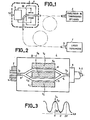
- the transient analyzer system comprises a single-mode laser 1 connected by a single-mode fiber 3 to the input of an optical transient analyzer device 2.
- the coherent source 1 emits continuously and the signal to be analyzed SA is used in an intermediate circuit 6 to modulate the light intensity in the fiber 3.
- This intermediate circuit 6 constitutes an interface circuit or an adapter device; it essentially comprises an amplitude modulator circuit 4 made of integrated optics and which makes it possible to modulate the light intensity of the optical signal as a function of the variations presented by an electrical input signal SE applied to circuit 4.
- the signal to be analyzed SA is in electrical form, it is applied directly to circuit 4; if, on the other hand, it is not electric, nor obviously not optical either, which is excluded in the configuration presented, it is applied beforehand to a complementary circuit 5 which translates it into electric form SE usable by the light intensity modulator circuit 4 .
- the light intensity modulator circuit may be constituted in a known manner by an interferometer with two arms, the structure of which is shown in FIG. 2. It is noted that the single-mode fiber 3 is in fact made up of three elements, an element 3.1 which connects the interferometer at the laser source 1 and an element 3.2 which then connects this interferometer to the analyzer 2.
- the circuit 6 comprises optical coupler devices 7 and 8 for coupling the ends of the single-mode fibers 3.1 and 3.2 respectively to the input and at the output of the two-arm interferometer.
- This interfero meter comprises a branch 11 of a single-mode waveguide in which a light wave of intensity I E circulates; this branch 11 is divided into two parallel arms 12 and 13 which then meet to form an outlet branch 14 where an intensity IS can be recovered.
- the directions of light propagation are the same in the four guides. Electrodes are arranged between the guides 12 and 13, electrode E M , and on either side of these two electrode guides E 2 and E 3 .
- the electrode E M is connected to the ground potential VM and voltages V2 and V3 are applied to the electrodes E 2 and E 3 .
- the arrangement of the electrodes adjacent to the guides causes in them electric fields perpendicular to the direction of propagation of the light waves.
- the entire device is produced on the surface of a substrate having electro-optical properties.
- the electric fields are in opposite directions and cause variations of opposite sign in the propagation speeds of the light waves in the two arms.
- the difference between the propagation speeds is proportional to the sum of the amplitudes of the electric fields applied, that is to say substantially proportional to the sum of the voltages V2 and V3.
- a phase difference is obtained between the two waves which were originally in phase.
- the intensity IS recovered varies as a function of the phase shift according to a sinusoidal law represented in FIG. 3, the intensity of which varies between a minimum Im and a maximum IM, the modulation rate IM / Im being a function of the coupling losses and of the asymmetry of the device.
- the signal SE is superimposed on one of the voltages V2 or V3 which are originally at the same potential V.
- the intensity IS follows the modulation provided that the phase shift remains between 2n ⁇ and between (2n + 1) ⁇ so as to keep a constant curve slope. Note that this sinusoidal response can be linearized by adding an optoelectronic feedback loop according to the technique described in French patent publication FR-A-2 453 426.
- Figures 4 to 6 relate to examples of use of the system in various cases where the signal to be analyzed SA is not of an electrical nature.
- the signal to be analyzed is a magnetic field H and the input circuit 5 is constituted by a coil L in which the field H induces a current which results in an electrical signal SE usable by the circuit. modulator 4.
- the signal to be analyzed is an electric field and the input circuit 5 is formed by antennas A1 and A2.
- the signal to be analyzed is a force F and the circuit 5 of FIG. 1 is formed using a quartz Q.
- a preferred embodiment of the system of FIG. 1 has been partially represented using a two-arm interferometer 4 to modulate the light intensity in the single-mode fiber 3 and in which the optical transient analyzer 2 is constituted by a photonic sampler device derived from slit camera tubes and particularized in that it comprises at the input a photocathode 21 of small dimensions and in that its fluorescent screen 22 is directly coupled to a detector strip 23 in solid circuit.
- the optical transient analyzer 2 is constituted by a photonic sampler device derived from slit camera tubes and particularized in that it comprises at the input a photocathode 21 of small dimensions and in that its fluorescent screen 22 is directly coupled to a detector strip 23 in solid circuit.
- concentration and focusing electrodes which receive high voltages HT1, HT2, an anode electrode supplied by a very high voltage THT and deflection electrodes 25 receiving deflection signals SD to produce scanning in the direction of the bar.
- the bar 23 is associated with circuits amplification and playback 24 which provide the detected
Landscapes
- Physics & Mathematics (AREA)
- General Physics & Mathematics (AREA)
- Investigating Or Analysing Materials By Optical Means (AREA)
Abstract
Description
- La présente invention concerne un système analyseur de transitoires rapides, les signaux à analyser pouvant avoir une durée comprise, par exemple, entre 30 picosecondes et quelques nano- secondes.
- Pour l'analyse de signaux très rapides, il est connu d'utiliser comme dispositif analyseur une caméra à balayage de fente associée à une caméra de télévision en circuit solide. La caméra à balayage de fente reçoit le signal à analyser sous forme optique. Si le signal est d'une autre nature, électrique par exemple, il est d'abord traité dans un circuit interface d'entrée qui le transforme en signal optique calibré. Les différents signaux optiques à traiter sont transmis par l'intermédiaire d'une optique à fibres à la caméra à balayage de fente, dite streak caméra en terminologie anglo-saxonne. Cette optique intermédiaire peut être constituée par des fibres juxtaposées linéairement pour former la fente lumineuse sur la photocathode d'entrée. Des électrodes déflectrices sont commandées pour produire un balayage perpendiculaire à la ligne résultant des N voies optiques juxtaposées sur un écran fluorescent en sortie du tube. L'image résultante formée de N traces verticales permet ensuite, par analyse à l'aide de la caméra de télévision et d'un circuit de traitement, d'étudier la variation temporelle des signaux correspondants.
- Dans la demande de brevet français n° 84 19196 du 14/12/84 il est décrit un dispositif échantillonneur photonique dérivé des caméras à fente et aménagé de manière à traiter une voie optique d'analyse à l'entrée. Suivant cette solution, le tube comporte à l'entrée une photocathode de dimensions réduites et est associé directement à un dispositif détecteur d'image en circuit solide constitué par une simple barrette détectrice orientée suivant la trace lumineuse à détecter. L'ensemble est réalisable de manière plus compacte et présente de multiples avantages, notamment du fait que le nombre d'échantillons correspondant au nombre d'éléments de la barrette détectrice est plus élevé que celui fourni par une matrice en circuit solide.
- Le but de l'invention est de réaliser un système analyseur de transitoires pour lequel le signal à analyser peut être électrique ou, s'il n'est pas électrique ni optique, est transformé préliminairement en signal électrique avant d'être fourni à l'analyseur sous forme optique, lequel dispositif d'analyse étant avantageusement du type précité répondant à l'analyse d'une voie unique.
- Suivant l'invention il est proposé de réaliser le système analyseur avec un dispositif adaptateur qui transforme le signal à analyser en signal lumineux, un conducteur de lumière à fibre permettant de transmettre le signal lumineux à l'entrée d'un dispositif analyseur de transitoires optiques ; le conducteur de lumière utilisé est une fibre monomode qui relie la sortie d'une source laser monomode à l'entrée du dispositif analyseur de transitoires optiques et le dispositif adaptateur comporte un modulateur d'amplitude en optique intégrée pour moduler l'intensité du signal tumineux en fonction d'un signal électrique appliqué au modulateur. Dans le cas où le signal à analyser n'est ni électrique ni optique, le dispositif adaptateur comporte des moyens complémentaires pour transformer ce signal à analyser en signal électrique de modulation.
- Les particularités et avantages de la présente invention apparaîtront dans la description qui suit donnée à titre d'exemple, à l'aide des figures annexées qui représentent :
- - Fig.l, un diagramme général d'un système d'analyse de transitoires conforme à l'invention ;
- - Fig.2, un schéma d'un interféromètre à deux bras de type connu, utilisable comme modulateur d'intensité lumineuse dans le système selon la figure 1 ;
- - Fig.3, la courbe de réponse de l'interféromètre selon la figure 2 ;
- - Fig.4, un mode de réalisation du circuit modulateur d'intensité lumineuse sous forme d'un capteur de champ magnétique ;
- - Fig.5, un deuxième mode de réalisation du circuit modulateur d'intensité lumineuse sous forme d'un capteur de champ électrique ;
- - Fig.6, un troisième mode de réalisation du circuit modulateur d'intensité lumineuse sous forme d'un capteur de pression ;
- - Fig.7, une représentation partielle d'un mode de réalisation du système d'analyse de transitoires selon la figure 1 utilisant un interféromètre selon la figure 2 et un tube échantillonneur photonique comme analyseur de transitoires optiques.
- En se reportant à la figure 1 le système analyseur de transitoires comporte un laser monomode 1 relié par une fibre monomode 3 à l'entrée d'un dispositif analyseur de transitoires optiques 2. La source cohérente 1 émet de manière continue et le signal à analyser SA est utilisé dans un circuit intermédiaire 6 pour moduler l'intensité lumineuse dans la fibre 3. Ce circuit intermédiaire 6 constitue un circuit d'interface ou un dispositif adaptateur ; il comporte essentiellement un circuit modulateur d'amplitude 4 réalisé en optique intégrée et qui permet de moduler l'intensité lumineuse du signal optique en fonction des variations présentées par un signal électrique d'entrée SE appliqué au circuit 4. Si le signal à analyser SA est sous forme électrique, il est appliqué directement au circuit 4 ; si par contre il n'est pas électrique, ni évidemment non plus optique ce qui est exclu dans la configuration présentée, il est appliqué préalablement à un circuit complémentaire 5 qui le traduit sous forme électrique SE utilisable par le circuit modulateur d'intensité lumineuse 4.
- Le circuit modulateur d'intensité lumineuse pourra être constitué de manière connue par un interféromètre à deux bras dont la structure est rappelée sur la figure 2. On note que la fibre monomode 3 est constituée en fait de trois éléments, un élément 3.1 qui relie l'interféromètre à la source laser 1 et un élément 3.2 qui relie cet interféromètre ensuite à l'analyseur 2. Le circuit 6 comporte des dispositifs coupleurs optiques 7 et 8 pour coupler convenablement les extrémités des fibres monomodes 3.1 et 3.2 respectivement à l'entrée et à la sortie de l'interféromètre à deux bras. Cet interféromètre comporte une branche 11 de guide d'onde monomode dans laquelle circule une onde lumineuse d'intensité IE ; cette branche 11 se divise en deux bras parallèles 12 et 13 qui se rejoignent ensuite pour former une branche 14 de sortie où l'on peut récupérer une intensité IS. Les directions de propagation de la lumière sont les mêmes dans les quatre guides. Des électrodes sont disposées entre les guides 12 et 13, électrode EM, et de part et d'autre de ces deux guides électrodes E2 et E3. L'électrode EM est raccordé au potentiel VM de masse et des tensions V2 et V3 sont appliquées aux électrodes E2 et E3. La disposition des électrodes adjacentes aux guides provoquent dans ceux-ci des champs électriques perpendiculaires à la direction de propagation des ondes lumineuses. L'ensemble du dispositif est réalisé à la surface d'un substrat possédant des propriétés électro-optiques. Pour des tensions V2 et V3 de même signe, les champs électriques sont de sens opposé et provoquent des variations de signe opposé dans les vitesses de propagation des ondes lumineuses dans les deux bras. La différence entre les vitesses de propagation est proportionnelle à la somme des amplitudes des champs électriques appliqués, c'est-à-dire sensiblement proportionnelle à la somme des tensions V2 et V3. On obtient à la sortie un déphasage entre les deux ondes qui se trouvaient primitivement en phase. L'intensité IS récupérée varie en fonction du déphasage selon une loi sinusoïdale représentée sur la figure 3 dont l'intensité varie entre un minimum Im et un maximum IM, le taux de modulation IM/Im étant fonction des pertes de couplage et de la dissymétrie du dispositif. Dans l'application considérée le signal SE est superposé à l'une des tensions V2 ou V3 qui sont originellement à un même potentiel V. Pour un signal SE analogique, l'intensité IS suit la modulation à condition que le déphasage reste compris entre 2n π et entre (2n+1) π de façon à conserver une pente de courbe constante. A noter que cette réponse sinusoïdale peut être linéarisée en ajoutant une boucle de rétroaction optoélectronique selon la technique décrite dans la publication de brevet français FR-A-2 453 426.
- Les figures 4 à 6 se rapportent à des exemples d'utilisation du système dans divers cas où le signal à analyser SA n'est pas de nature électrique.
- Dans l'exemple de la figure 4 le signal à analyser est un champ magnétique H et le circuit 5 d'entrée est constitué par une bobine L dans laquelle le champ H induit un courant qui se traduit par un signal électrique SE utilisable par le circuit modulateur 4.
- Dans le cas de la figure 5, le signal à analyser est un champ électrique et le circuit d'entrée 5 est formé par des antennes Al et A2.
- Dans le cas de la figure 6 le signal à analyser est une force F et le circuit 5 de la figure 1 est constitué à l'aide d'un quartz Q.
- On remarque que les montages proposés selon les figures 4 à 6, ainsi que d'autres montages possibles pour d'autres natures de signal à analyser, permettent de constituer un dispositif capteur de mesure 6 aisément déplaçable du fait qu'il est relié au circuit annexe 1 et 2 par l'intermédiaire d'une fibre optique, que ce capteur est isolé électriquement, qu'il est miniaturisé et qu'il est passif étant donné qu'il ne nécessite aucune alimentation.
- Dans la représentation figure 7 on a représenté partiellement une réalisation préférée du système de la figure 1 en utilisant un interféromètre à deux bras 4 pour moduler l'intensité lumineuse dans la fibre monomode 3 et dans lequel l'analyseur de transitoires optiques 2 est constitué par un dispositif échantillonneur photonique dérivé des tubes caméras à fente et particularisé en ce qu'il comporte à l'entrée une photocathode 21 de faibles dimensions et en ce que son écran fluorescent 22 est couplé directement à une barrette détectrice 23 en circuit solide. On distingue à l'intérieur du tube des électrodes de concentration et de focalisation qui reçoivent des hautes tensions HT1, HT2, une électrode d'anode alimentée par une très haute tension THT et des électrodes de déflexion 25 recevant des signaux de déflexion SD pour produire le balayage selon la direction de la barrette. La barrette 23 est associée à des circuits d'amplification et de lecture 24 qui fournissent le signal vidéo détecté SV. La lecture est synchronisée par un signal d'horloge locale HL.
Claims (9)
Applications Claiming Priority (2)
| Application Number | Priority Date | Filing Date | Title |
|---|---|---|---|
| FR8419361A FR2574943B1 (fr) | 1984-12-18 | 1984-12-18 | Systeme analyseur de transitoires |
| FR8419361 | 1984-12-18 |
Publications (2)
| Publication Number | Publication Date |
|---|---|
| EP0187091A1 true EP0187091A1 (fr) | 1986-07-09 |
| EP0187091B1 EP0187091B1 (fr) | 1989-04-26 |
Family
ID=9310727
Family Applications (1)
| Application Number | Title | Priority Date | Filing Date |
|---|---|---|---|
| EP85402477A Expired EP0187091B1 (fr) | 1984-12-18 | 1985-12-12 | Système analyseur de transitoires |
Country Status (4)
| Country | Link |
|---|---|
| US (1) | US4719412A (fr) |
| EP (1) | EP0187091B1 (fr) |
| DE (1) | DE3569829D1 (fr) |
| FR (1) | FR2574943B1 (fr) |
Cited By (3)
| Publication number | Priority date | Publication date | Assignee | Title |
|---|---|---|---|---|
| FR2613838A1 (fr) * | 1987-04-10 | 1988-10-14 | Alsthom | Dispositif de mesure d'intensite d'un courant electrique par effet faraday mis en oeuvre au sein d'un interferometre de sagnac |
| EP0664460A4 (fr) * | 1993-07-07 | 1996-09-11 | Tokin Corp | Capteur de champs electriques. |
| EP0668507A4 (fr) * | 1993-07-07 | 1996-09-11 | Tokin Corp | Capteur de champs electriques. |
Families Citing this family (18)
| Publication number | Priority date | Publication date | Assignee | Title |
|---|---|---|---|---|
| JPS6225727A (ja) * | 1985-07-03 | 1987-02-03 | ウエスチングハウス エレクトリック コ−ポレ−ション | 光学コンパレ−タ |
| GB2192272B (en) * | 1986-07-02 | 1990-06-06 | Cossor Electronics Ltd | Spectrum analyser |
| US4810978A (en) * | 1987-06-29 | 1989-03-07 | Hughes Aircraft Company | Optical data link |
| US4918373A (en) * | 1988-03-18 | 1990-04-17 | Hughes Aircraft Company | R.F. phase noise test set using fiber optic delay line |
| US5060225A (en) * | 1988-11-14 | 1991-10-22 | Hughes Aircraft Company | Phase modulated optical carrier data link for a focal plane array |
| DE602004030914D1 (de) * | 2003-07-14 | 2011-02-17 | Photonicsystems Inc | Bidirektionale signalschnittstelle |
| DE102004036309A1 (de) * | 2004-07-27 | 2006-03-23 | Dorma Gmbh + Co. Kg | An einem vertikalen Rahmenprofil eines Türflügels angeordnete Dichtung |
| US7809216B2 (en) * | 2007-03-16 | 2010-10-05 | Photonic Systems, Inc. | Bi-directional signal interface and apparatus using same |
| US8731410B2 (en) * | 2007-10-02 | 2014-05-20 | Luxtera, Inc. | Method and system for split voltage domain receiver circuits |
| US8755750B2 (en) | 2010-05-22 | 2014-06-17 | Photonic Systems, Inc. | Wide-bandwidth signal canceller |
| US9935680B2 (en) | 2012-07-30 | 2018-04-03 | Photonic Systems, Inc. | Same-aperture any-frequency simultaneous transmit and receive communication system |
| US9209840B2 (en) | 2012-07-30 | 2015-12-08 | Photonic Systems, Inc. | Same-aperture any-frequency simultaneous transmit and receive communication system |
| US11539392B2 (en) | 2012-07-30 | 2022-12-27 | Photonic Systems, Inc. | Same-aperture any-frequency simultaneous transmit and receive communication system |
| US10374656B2 (en) | 2012-07-30 | 2019-08-06 | Photonic Systems, Inc. | Same-aperture any-frequency simultaneous transmit and receive communication system |
| US10158432B2 (en) | 2015-10-22 | 2018-12-18 | Photonic Systems, Inc. | RF signal separation and suppression system and method |
| US10623986B2 (en) | 2015-10-22 | 2020-04-14 | Photonic Systems, Inc. | RF signal separation and suppression system and method |
| WO2025089056A1 (fr) * | 2023-10-26 | 2025-05-01 | 浜松ホトニクス株式会社 | Dispositif d'inspection de semi-conducteur et procédé d'inspection de semi-conducteur |
| WO2025089055A1 (fr) * | 2023-10-26 | 2025-05-01 | 浜松ホトニクス株式会社 | Dispositif de mesure de signal électrique et procédé de mesure de signal électrique |
Citations (2)
| Publication number | Priority date | Publication date | Assignee | Title |
|---|---|---|---|---|
| FR2508754A1 (fr) * | 1981-06-25 | 1982-12-31 | Comp Generale Electricite | Hydrophone a fibre optique avec capteur immerge passif |
| DE3127406A1 (de) * | 1981-07-10 | 1983-01-27 | Siemens Ag | Elektrooptischer modulator mit einem monomodelichtwellenleitermodulator |
Family Cites Families (9)
| Publication number | Priority date | Publication date | Assignee | Title |
|---|---|---|---|---|
| US4253060A (en) * | 1979-05-29 | 1981-02-24 | Hughes Aircraft Company | RF Spectrum analyzer |
| US4348074A (en) * | 1980-03-03 | 1982-09-07 | The United States Of America As Represented By The Secretary Of The Navy | Application of ion implantation to LiNbO3 integrated, optical spectrum analyzers |
| US4394060A (en) * | 1981-04-15 | 1983-07-19 | Canon Kabushiki Kaisha | Light beam scanning system with saw transducer |
| US4446425A (en) * | 1982-02-12 | 1984-05-01 | The University Of Rochester | Measurement of electrical signals with picosecond resolution |
| SE431260B (sv) * | 1982-06-02 | 1984-01-23 | Asea Ab | Fiberoptiskt metdon for metning av elektriska och magnetiska storheter |
| US4456877A (en) * | 1982-09-16 | 1984-06-26 | Ampex Corporation | Hybrid spectrum analyzer system |
| DE3404822A1 (de) * | 1984-02-10 | 1985-08-14 | Siemens AG, 1000 Berlin und 8000 München | Braggzellen-spektralanalysator mit einem prismenaufweitungssystem |
| US4603293A (en) * | 1984-03-27 | 1986-07-29 | University Of Rochester | Measurement of electrical signals with subpicosecond resolution |
| US4633170A (en) * | 1984-06-05 | 1986-12-30 | The United States Of America As Represented By The Secretary Of The Navy | Bragg cell spectrum analyzer |
-
1984
- 1984-12-18 FR FR8419361A patent/FR2574943B1/fr not_active Expired
-
1985
- 1985-12-10 US US06/807,461 patent/US4719412A/en not_active Expired - Fee Related
- 1985-12-12 EP EP85402477A patent/EP0187091B1/fr not_active Expired
- 1985-12-12 DE DE8585402477T patent/DE3569829D1/de not_active Expired
Patent Citations (2)
| Publication number | Priority date | Publication date | Assignee | Title |
|---|---|---|---|---|
| FR2508754A1 (fr) * | 1981-06-25 | 1982-12-31 | Comp Generale Electricite | Hydrophone a fibre optique avec capteur immerge passif |
| DE3127406A1 (de) * | 1981-07-10 | 1983-01-27 | Siemens Ag | Elektrooptischer modulator mit einem monomodelichtwellenleitermodulator |
Non-Patent Citations (3)
| Title |
|---|
| 1980 IEEE MTT-S INTERNATIONAL MICROWAVE SYMPOSIUM DIGEST, catalogue no. 77-645125, 1980, pages 317-318, IEEE, New York, US; H.I. BASSEN et al.: "An RF field strength measurement system using an integrated optical linear modulator * |
| ADVANCES IN INSTRUMENTATION, vol. 37, partie 3, 1982, pages 1655-1671, ISA, Research Triangle Park, US; A.R. TEBO: "Sensing with optical fibers: an emerging technology" * |
| IBM TECHNICAL DISCLOSURE BULLETIN, vol. 26, no. 12, mai 1984, pages 6604-6605, New York, US; J.A. KASH: "Picosecond streak camera with single photon sensitivity" * |
Cited By (7)
| Publication number | Priority date | Publication date | Assignee | Title |
|---|---|---|---|---|
| FR2613838A1 (fr) * | 1987-04-10 | 1988-10-14 | Alsthom | Dispositif de mesure d'intensite d'un courant electrique par effet faraday mis en oeuvre au sein d'un interferometre de sagnac |
| EP0290780A1 (fr) * | 1987-04-10 | 1988-11-17 | Alsthom | Dispositif de mesure d'intensité d'un courant électrique par effet Faraday mis en oeuvre au sein d'un interféromètre de Sagnac |
| EP0664460A4 (fr) * | 1993-07-07 | 1996-09-11 | Tokin Corp | Capteur de champs electriques. |
| EP0668507A4 (fr) * | 1993-07-07 | 1996-09-11 | Tokin Corp | Capteur de champs electriques. |
| US5625284A (en) * | 1993-07-07 | 1997-04-29 | Tokin Corporation | Electric field sensor having sensor head with unbalanced electric field shield to shield branched optical waveguides against an applied electric field |
| US5781003A (en) * | 1993-07-07 | 1998-07-14 | Tokin Corporation | Electric field sensor |
| US5850140A (en) * | 1993-07-07 | 1998-12-15 | Tokin Corporation | Electric field sensor having sensor head with unbalanced electric field shield to shield branched optical waveguides against an applied electric field |
Also Published As
| Publication number | Publication date |
|---|---|
| DE3569829D1 (en) | 1989-06-01 |
| FR2574943A1 (fr) | 1986-06-20 |
| US4719412A (en) | 1988-01-12 |
| EP0187091B1 (fr) | 1989-04-26 |
| FR2574943B1 (fr) | 1987-05-22 |
Similar Documents
| Publication | Publication Date | Title |
|---|---|---|
| EP0187091B1 (fr) | Système analyseur de transitoires | |
| US7289197B2 (en) | Transmissive optical detector | |
| CN101526398B (zh) | 太赫分光计 | |
| EP0231015B1 (fr) | Dispositif de télécommunications photoniques cohérentes | |
| US5003268A (en) | Optical signal sampling apparatus | |
| EP0187087B1 (fr) | Dispositif échantillonneur photonique et système d'analyse de transitoires utilisant un tel dispositif | |
| JPS61116634A (ja) | 光フアイバの伝送特性を計測する装置 | |
| EP0744844B1 (fr) | Procédé d'inscription de données binaires sur une onde porteuse, notamment optique, et système de transmission utilisant ce procédé | |
| JPH08152361A (ja) | 光信号波形の測定装置 | |
| Hegarty et al. | Low-loss single-mode wavelength-division multiplexing with etched fibre arrays | |
| JP2659554B2 (ja) | 光強度相関装置 | |
| JPH11337589A (ja) | 電気光学サンプリングオシロスコープ用プローブ | |
| RU2112318C1 (ru) | Способ и схема для электрической компенсации искажений сигнала | |
| US4156809A (en) | Data acquisition system | |
| Costa et al. | Attenuation measurements performed by backscattering technique | |
| EP1723705A1 (fr) | Dispositif de decalage de frequence dans un chemin optique a source laser continue | |
| CN108418633A (zh) | 瞬态脉冲电信号光纤传输系统 | |
| JP2582588B2 (ja) | 多チャンネル電圧検出装置 | |
| JP3313492B2 (ja) | 光波形測定装置 | |
| JP2001228021A (ja) | 光信号測定回路 | |
| EP0795778A1 (fr) | Dispositif optique non-linéaire de traitement de signaux optiques | |
| McWright et al. | Integrated optical devices for photonics instrumentation systems | |
| Yaita et al. | Ultrafast optical pulse-pattern signal measurement using optoelectronic techniques | |
| JP3271299B2 (ja) | 光周波数切替特性測定装置 | |
| FR2859795A1 (fr) | Convertisseur electro-optique et dispositif de connexion de type bidirectionnel comportant un tel convertisseur |
Legal Events
| Date | Code | Title | Description |
|---|---|---|---|
| PUAI | Public reference made under article 153(3) epc to a published international application that has entered the european phase |
Free format text: ORIGINAL CODE: 0009012 |
|
| AK | Designated contracting states |
Kind code of ref document: A1 Designated state(s): CH DE GB IT LI |
|
| 17P | Request for examination filed |
Effective date: 19861217 |
|
| 17Q | First examination report despatched |
Effective date: 19880915 |
|
| GRAA | (expected) grant |
Free format text: ORIGINAL CODE: 0009210 |
|
| AK | Designated contracting states |
Kind code of ref document: B1 Designated state(s): CH DE GB IT LI |
|
| ITF | It: translation for a ep patent filed | ||
| RAP4 | Party data changed (patent owner data changed or rights of a patent transferred) |
Owner name: THOMSON-CSF |
|
| REF | Corresponds to: |
Ref document number: 3569829 Country of ref document: DE Date of ref document: 19890601 |
|
| GBT | Gb: translation of ep patent filed (gb section 77(6)(a)/1977) | ||
| PLBE | No opposition filed within time limit |
Free format text: ORIGINAL CODE: 0009261 |
|
| STAA | Information on the status of an ep patent application or granted ep patent |
Free format text: STATUS: NO OPPOSITION FILED WITHIN TIME LIMIT |
|
| 26N | No opposition filed | ||
| ITTA | It: last paid annual fee | ||
| PGFP | Annual fee paid to national office [announced via postgrant information from national office to epo] |
Ref country code: CH Payment date: 19951114 Year of fee payment: 11 |
|
| PGFP | Annual fee paid to national office [announced via postgrant information from national office to epo] |
Ref country code: DE Payment date: 19951120 Year of fee payment: 11 |
|
| PGFP | Annual fee paid to national office [announced via postgrant information from national office to epo] |
Ref country code: GB Payment date: 19951121 Year of fee payment: 11 |
|
| PG25 | Lapsed in a contracting state [announced via postgrant information from national office to epo] |
Ref country code: GB Effective date: 19961212 |
|
| PG25 | Lapsed in a contracting state [announced via postgrant information from national office to epo] |
Ref country code: LI Effective date: 19961231 Ref country code: CH Effective date: 19961231 |
|
| GBPC | Gb: european patent ceased through non-payment of renewal fee |
Effective date: 19961212 |
|
| REG | Reference to a national code |
Ref country code: CH Ref legal event code: PL |
|
| PG25 | Lapsed in a contracting state [announced via postgrant information from national office to epo] |
Ref country code: DE Effective date: 19970902 |