EP0187412B1 - Tube à rayons cathodiques monochrome - Google Patents
Tube à rayons cathodiques monochrome Download PDFInfo
- Publication number
- EP0187412B1 EP0187412B1 EP85202014A EP85202014A EP0187412B1 EP 0187412 B1 EP0187412 B1 EP 0187412B1 EP 85202014 A EP85202014 A EP 85202014A EP 85202014 A EP85202014 A EP 85202014A EP 0187412 B1 EP0187412 B1 EP 0187412B1
- Authority
- EP
- European Patent Office
- Prior art keywords
- faceplate
- screen
- filter
- wavelength
- edge filter
- Prior art date
- Legal status (The legal status is an assumption and is not a legal conclusion. Google has not performed a legal analysis and makes no representation as to the accuracy of the status listed.)
- Expired - Lifetime
Links
- 239000000463 material Substances 0.000 claims description 16
- 230000003287 optical effect Effects 0.000 claims description 14
- 125000001475 halogen functional group Chemical group 0.000 claims description 12
- 238000010894 electron beam technology Methods 0.000 claims description 9
- 230000005855 radiation Effects 0.000 claims description 6
- 238000000149 argon plasma sintering Methods 0.000 claims description 2
- 239000012780 transparent material Substances 0.000 claims description 2
- OAICVXFJPJFONN-UHFFFAOYSA-N Phosphorus Chemical compound [P] OAICVXFJPJFONN-UHFFFAOYSA-N 0.000 description 8
- 239000011248 coating agent Substances 0.000 description 7
- 238000000576 coating method Methods 0.000 description 7
- 238000002834 transmittance Methods 0.000 description 6
- 150000001875 compounds Chemical class 0.000 description 5
- 239000011521 glass Substances 0.000 description 3
- 238000002310 reflectometry Methods 0.000 description 3
- 239000004411 aluminium Substances 0.000 description 2
- XAGFODPZIPBFFR-UHFFFAOYSA-N aluminium Chemical compound [Al] XAGFODPZIPBFFR-UHFFFAOYSA-N 0.000 description 2
- 229910052782 aluminium Inorganic materials 0.000 description 2
- 238000010276 construction Methods 0.000 description 2
- 239000010409 thin film Substances 0.000 description 2
- NFACJZMKEDPNKN-UHFFFAOYSA-N trichlorfon Chemical compound COP(=O)(OC)C(O)C(Cl)(Cl)Cl NFACJZMKEDPNKN-UHFFFAOYSA-N 0.000 description 2
- VYPSYNLAJGMNEJ-UHFFFAOYSA-N Silicium dioxide Chemical compound O=[Si]=O VYPSYNLAJGMNEJ-UHFFFAOYSA-N 0.000 description 1
- GWEVSGVZZGPLCZ-UHFFFAOYSA-N Titan oxide Chemical compound O=[Ti]=O GWEVSGVZZGPLCZ-UHFFFAOYSA-N 0.000 description 1
- 239000005083 Zinc sulfide Substances 0.000 description 1
- 230000002411 adverse Effects 0.000 description 1
- 238000013459 approach Methods 0.000 description 1
- 239000004020 conductor Substances 0.000 description 1
- 230000003247 decreasing effect Effects 0.000 description 1
- ORUIBWPALBXDOA-UHFFFAOYSA-L magnesium fluoride Chemical compound [F-].[F-].[Mg+2] ORUIBWPALBXDOA-UHFFFAOYSA-L 0.000 description 1
- 229910001635 magnesium fluoride Inorganic materials 0.000 description 1
- 238000013021 overheating Methods 0.000 description 1
- BPUBBGLMJRNUCC-UHFFFAOYSA-N oxygen(2-);tantalum(5+) Chemical compound [O-2].[O-2].[O-2].[O-2].[O-2].[Ta+5].[Ta+5] BPUBBGLMJRNUCC-UHFFFAOYSA-N 0.000 description 1
- 239000002245 particle Substances 0.000 description 1
- 230000035515 penetration Effects 0.000 description 1
- 229910052814 silicon oxide Inorganic materials 0.000 description 1
- 230000003595 spectral effect Effects 0.000 description 1
- 239000000758 substrate Substances 0.000 description 1
- 229910001936 tantalum oxide Inorganic materials 0.000 description 1
- OGIDPMRJRNCKJF-UHFFFAOYSA-N titanium oxide Inorganic materials [Ti]=O OGIDPMRJRNCKJF-UHFFFAOYSA-N 0.000 description 1
- 229910052984 zinc sulfide Inorganic materials 0.000 description 1
- DRDVZXDWVBGGMH-UHFFFAOYSA-N zinc;sulfide Chemical compound [S-2].[Zn+2] DRDVZXDWVBGGMH-UHFFFAOYSA-N 0.000 description 1
Images

Classifications
-
- H—ELECTRICITY
- H01—ELECTRIC ELEMENTS
- H01J—ELECTRIC DISCHARGE TUBES OR DISCHARGE LAMPS
- H01J29/00—Details of cathode-ray tubes or of electron-beam tubes of the types covered by group H01J31/00
- H01J29/86—Vessels; Containers; Vacuum locks
- H01J29/89—Optical or photographic arrangements structurally combined or co-operating with the vessel
-
- G—PHYSICS
- G02—OPTICS
- G02B—OPTICAL ELEMENTS, SYSTEMS OR APPARATUS
- G02B5/00—Optical elements other than lenses
- G02B5/20—Filters
- G02B5/28—Interference filters
- G02B5/285—Interference filters comprising deposited thin solid films
-
- G—PHYSICS
- G02—OPTICS
- G02B—OPTICAL ELEMENTS, SYSTEMS OR APPARATUS
- G02B6/00—Light guides; Structural details of arrangements comprising light guides and other optical elements, e.g. couplings
- G02B6/04—Light guides; Structural details of arrangements comprising light guides and other optical elements, e.g. couplings formed by bundles of fibres
- G02B6/06—Light guides; Structural details of arrangements comprising light guides and other optical elements, e.g. couplings formed by bundles of fibres the relative position of the fibres being the same at both ends, e.g. for transporting images
- G02B6/08—Light guides; Structural details of arrangements comprising light guides and other optical elements, e.g. couplings formed by bundles of fibres the relative position of the fibres being the same at both ends, e.g. for transporting images with fibre bundle in form of plate
-
- H—ELECTRICITY
- H01—ELECTRIC ELEMENTS
- H01J—ELECTRIC DISCHARGE TUBES OR DISCHARGE LAMPS
- H01J29/00—Details of cathode-ray tubes or of electron-beam tubes of the types covered by group H01J31/00
- H01J29/02—Electrodes; Screens; Mounting, supporting, spacing or insulating thereof
- H01J29/10—Screens on or from which an image or pattern is formed, picked up, converted or stored
- H01J29/18—Luminescent screens
- H01J29/185—Luminescent screens measures against halo-phenomena
-
- H—ELECTRICITY
- H01—ELECTRIC ELEMENTS
- H01J—ELECTRIC DISCHARGE TUBES OR DISCHARGE LAMPS
- H01J2229/00—Details of cathode ray tubes or electron beam tubes
- H01J2229/89—Optical components associated with the vessel
- H01J2229/8907—Image projection devices
-
- H—ELECTRICITY
- H01—ELECTRIC ELEMENTS
- H01J—ELECTRIC DISCHARGE TUBES OR DISCHARGE LAMPS
- H01J2229/00—Details of cathode ray tubes or electron beam tubes
- H01J2229/89—Optical components associated with the vessel
- H01J2229/8913—Anti-reflection, anti-glare, viewing angle and contrast improving treatments or devices
- H01J2229/8916—Anti-reflection, anti-glare, viewing angle and contrast improving treatments or devices inside the vessel
-
- H—ELECTRICITY
- H01—ELECTRIC ELEMENTS
- H01J—ELECTRIC DISCHARGE TUBES OR DISCHARGE LAMPS
- H01J2229/00—Details of cathode ray tubes or electron beam tubes
- H01J2229/89—Optical components associated with the vessel
- H01J2229/8913—Anti-reflection, anti-glare, viewing angle and contrast improving treatments or devices
- H01J2229/8918—Anti-reflection, anti-glare, viewing angle and contrast improving treatments or devices by using interference effects
-
- H—ELECTRICITY
- H01—ELECTRIC ELEMENTS
- H01J—ELECTRIC DISCHARGE TUBES OR DISCHARGE LAMPS
- H01J2229/00—Details of cathode ray tubes or electron beam tubes
- H01J2229/89—Optical components associated with the vessel
- H01J2229/893—Optical components associated with the vessel using lenses
Definitions
- This invention relates to a monochromatic cathode ray tube having a faceplate arrangement including a faceplate consisting essentially of a transparent material, an internal screen consisting essentially of a light scattering luminescent material for emitting light radiation in a band encompassing a predetermined wavelength ⁇ 0 and extending from a lower wavelength ⁇ - 0 to an upper wavelength ⁇ + 0 , when excited by an electron beam, an electrically-conductive reflective layer disposed on an inner surface of the screen, and an optical filter disposed between the screen and the faceplate.
- U.S. Patent 4,310,784 to Anthon et al discloses a cathode ray tube faceplate construction for suppressing halo.
- the construction consists of a clear glass faceplate having an anti-reflection coating on its outside surface and an angle-sensitive thin film interference coating between its inside surface and a phosphor screen.
- the outside antireflection coating is provided to reduce reflection back into the faceplate of luminescent light rays incident thereto at small angles, thereby suppressing a central portion of halo surrounding a luminescent spot.
- the inside interference coating is provided to reflect luminescent light rays incident thereto at large angles, thereby suppressing a ringlike outer portion of the halo surrounding the central portion.
- optical filter includes:
- the invention is based on the insight that the image quality can be improved by providing a monochromatic cathode ray tube with a faceplate arrangement including optical filter means which blocks substantially all visually perceptible light radiation incident at angles above ⁇ H , and which passes substantially all such light radiation incident at angles below ⁇ H , such that the optical filter means also operates as a band-pass filter.
- the filter then blocks all visually perceptible light radiation having wavelengths outside a monochromatic band of light radiation in a bandwidth encompassing the principal wavelength ⁇ 0 which the tube is intended to produce, (e.g. red, green, blue) and extending from a lower wavelength ⁇ - 0 to an upper wavelength ⁇ + 0 .
- an inside interference coating should, by itself, effectively decrease halo and increase brightness.
- Such a coating should reflect back into the powdered luminescent screen all rays which would otherwise contribute to halo. Some of these reflected rays would be redirected toward the faceplate, increasing image brightness.
- the coating should operate as a filter having a sharp cutoff, reflecting all rays which significantly contribute to halo (i.e. rays emitted at angles larger than a predetermined angle ⁇ H ), and passing all rays emitted at smaller angles.
- Anthon's interference filter produces a gradual increase in reflectivity with angle, reaching only about 60 % reflectivity for rays incident at 45° while producing substantial reflectivity even for rays incident at angles between 0° and 30°.
- the filter in accordance with the invention includes a first portion adjacent the screen and a second portion adjacent the faceplate.
- the first portion comprising a multilayer interference edge filter having a cutoff wavelength equal to ⁇ + 0 for light rays received from the screen which are perpendicular to the edge filter, and having a cutoff wavelength equal to ⁇ + 0 for light rays received from the screen which are incident to the edge filter at angles greater than ⁇ H .
- the second portion of the compound filter comprises a multilayer matching filter for matching the optical impedances of the faceplate and the edge filter.
- the compound filter is highly transmissive for light rays incident at angles between 0° and ⁇ H which have wavelengths at or near the principal wavelength ⁇ 0 , and is highly reflective for all other visually perceptible light rays.
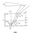
- Figure 1 is a sectional view of one end of a cathode ray tube faceplate and a lens in a projection system employing a prior art cathode ray tube;
- Figure 2 is a graph illustrating the optical characteristics of a cathode ray tube faceplate in accordance with the invention.
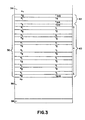
- Figure 3 is a sectional view of one end of a cathode ray tube faceplate arrangement in accordance with the invention.
- Figure 1 illustrates a typical prior art faceplate arrangement 10 of a projection tube spaced from a focusing lens 12, both shown in cross-section.
- the lens 12 magnifies the image formed by light rays received from the faceplate arrangement 10, and projects the image into a relatively large reflective or transmissive projection screen (not shown).
- the arrangement 10 includes a glass faceplate 14, a powdered luminescent screen 16 deposited onto the faceplate, and a reflective layer 18 of an electrically-conductive material such as aluminium. Typical thicknesses for the faceplate, the luminescent screen, and the reflective layer are 10 millimeters, 50 microns and 0.1 microns, respectively.
- the layer 18 is provided to collect excited electrons from the screen and to reflect toward the faceplate backwardly-directed light rays passing through the screen, thereby increasing the amount of light reaching the lens 12. As is subsequently explained, however, the layer 18 not only increases the amount of useful light reaching the lens 12, but also increases light contributing the halo.
- Figure 1 is not drawn to scale, it demonstrates how light rays emitted by the luminescent screen are transmitted through the faceplate arrangement 10.
- an electron beam 20 excites the luminescent screen 16 at a spot such as that centered on point 22, a multiplicity of light rays are emitted at different angles. All angles are measured relative to a line 24 originating at the point 22 and passing perpendicularly through a faceplate-screen interface 26 and a faceplate-air interface 28.
- All light rays emitted toward the interface 26 are at least partly reflected back into the powdered luminescent screen 16, as rays I B .
- These rays I B will be scattered in all directions by the particles in the luminescent screen.
- Those rays scattered toward the reflective layer 18 will be redirected toward the faceplate 14.
- the lateral shift between point 22 and any point at which one of these scattered rays is incident at the interface 26 is on the order of the thickness of the luminescent screen itself (e.g. 50 microns) and thus does not substantially increase the diameter of the luminescent electron beam spot, which is typically about 500 microns.
- the light rays emitted from point 22 which pass through the faceplate-screen interface 26 reach the faceplate-air interface 28 at the front of the tube. At least a portion I R of each ray reaching the interface 28 is reflected back toward the interface 26.
- the reflected rays I R reaching the interface 26 are laterally shifted from the point of origin 22 by distances on the order of the faceplate thickness (e.g. 10 millimeters). These laterally-shifted rays are back-scattered by the combination of the powdered luminescent material 16 and the reflective layer 18 and form a number of concentric ring-shaped halos around the image of the electron beam spot, causing decreased image contrast.
- Figure 2 illustrates both the emission characteristics of a typical luminescent screen and the desired transmittance of the interference edge filter forming the first portion of a filter means in accordance with the invention.
- the solid lines illustrate the spectral distribution of a high-brightness terbium-doped P44 phosphor material which emits visible light in four distinct bands, including a primary green emission band and three spurious emission bands.
- the spurious emission bands include a blue sideband to the left of the primary emission band, and orange and red sidebands to the right.
- the primary emission band has its peak intensity at 544 nanometers ( ⁇ 0 ) and extends from approximately 532 nanometers ( ⁇ - 0 ) to approximately 568 nanometers ( ⁇ + 0 ).
- the dashed-/dotted lines illustrate the desired transmittance characteristics of the edge filter.
- the edge filter is designed to have a cutoff wavelength of ⁇ + 0 for light rays incident to the filter at 900°.
- the edge filter is designed to have a cutoff wavelength of ⁇ - 0 for light rays incident to the filter at ⁇ H .
- the ideal transmittance characteristics illustrated by the dashed/dotted lines in Figure 2 cannot be obtained by use of the edge filter alone, but they can be closely approximated by the addition of the multilayer matching filter forming the second portion of the filter means.
- the matching filter reduces ripple in the transmittance characteristics, which is the major cause of deviation from the illustrated characteristics. This reduction is accomplished by providing a combination of layers having an equivalent admittance which matches the admittance of the edge filter to that of the faceplate material which serves as the supporting substrate for the compound filter. Suitable matching filters are described in the previously mentioned text by Macleod on pages 128-143.
- the above-described filter is highly transmissive for light in the spurious blue sideband. This light is not noticeable, however, because of the relatively low energy content of the sideband in comparison to that of the primary green band, and because of the low acuity of the human eye for blue light in comparison to green light.
- the spurious sidebands need not be con-. sidered, either because they fall in the rejection band or because no sidebands visible to the human eye are produced. Red light producing europium-doped materials and blue light producing thulium-doped materials are examples of phosphor materials which produce no visible sidebands.
- the faceplate arrangement includes a compound optical filter 32 deposited on the inner surface of a glass faceplate 34, a screen 36 consisting essentially of terbium-doped p44 green phosphor material deposited on the innermost layer of the filter 32, and a reflective aluminium layer 38 deposited on the inner surface of the screen.
- the thickness t and the refractive index n of each layer of the filter is indicated in the drawing figure.
- the refractive indices of the faceplate 34 and the screen 36 are also indicated.
- the faceplate and screen thicknesses depend on the size of the tube and the energy of the electron beam, but are typically on the order of 10 millimeters and 50 microns, respectively, for a projection tube, or 5-15 millimeters and 10-50 microns, respectively, for a display tube.
- the thickness, of the reflective layer 38 must be sufficiently small to enable penetration by the electron beam, but sufficiently large to conduct the electron beam current away from the screen without overheating. Typically this thickness is about 0.1 micron. ⁇ - ⁇
- the compound optical filter 39 includes a first portion 40 forming the interference edge filter and a second portion 42 forming the matching filter.
- the edge filter 40 includes a first layer adjacent the screen 36, an odd number m of intermediate layers, and a final layer adjacent the matching filter 42.
- the first layer has a refractive index n2 and a thickness t2/2.
- the m intermediate layers have alternate refractive indices and thicknesses n1 and t1, n2 and t2, respectively.
- the final layer of the edge filter 40 has the refractive index n2, and the thickness t2/2.
- the matching filter 42 has three layers, including a first layer having a thickness t3/2 which is adjacent the final layer of the edge filter. These two layers are indistinguishable from each other, as is indicated in Figure 3 by a dashed line, because both layers are formed from the same material having the refractive index n2.
- the second layer of the matching filter has the refractive index n1 and a thickness t4.
- the final layer of the matching filter is adjacent the faceplate 34 and has the refractive index n2, and the thickness t3/2.
- the layers in the edge filter and the matching filter also have the following relationships;
- This wave-length ⁇ MIN is the center wavelength of a rejection band of the edge filter which has a lower cutoff wavelength approximately equal to ⁇ + 0 and a bandwidth equal to ⁇ .
- the performance of the edge filter can also be optimized by increasing, up to a point, the number m of intermediate layers. Good performance can be obtained with as few as seven intermediate layers, while little improvement in performance is obtained by increasing the number of intermediate layers beyond 15.
- a faceplate arrangement having the above described layer materials and thicknesses, and 15 intermediate layers, closely approaches the transmittance characteristics illustrated in Figure 2 for ⁇ H 30°.
- the invention has been described with reference to a projection tube embodiment having a particular phosphor material, it may be easily adapted for use with other types of cathode ray tube, such as display tube, and with other phosphor materials.
Landscapes
- Physics & Mathematics (AREA)
- General Physics & Mathematics (AREA)
- Optics & Photonics (AREA)
- Cathode-Ray Tubes And Fluorescent Screens For Display (AREA)
- Transforming Electric Information Into Light Information (AREA)
Claims (3)
- Tube à rayons cathodiques monochrome ayant un ensemble de plaque frontale (10) comportant une plaque frontale (14, 34) consistant essentiellement en un matériau transparent, un écran interne (16, 36) consistant essentiellement en un matériau luminescent à dispersion lumineuse pour émettre un rayonnement lumineux dans une bande contenant une longueur d'onde prédéterminée λ0et s'étendant à partir d'une longueur d'onde inférieure λ

 a) une première partie (40) contiguë à l'écran et comportant un filtre de coupure interférentiel à couches multiples ayant une longueur d'onde de coupure de λ
 b) une deuxième partie (42) contiguë à la plaque frontale et comportant un filtre d'adaptation à couches multiples pour adapter les impédances optiques de la plaque frontale et du filtre de coupure, en ce que ledit filtre de coupure comporte:c) une première couche contiguë à l'écran et ayant un indice de réfraction n₂ et une épaisseur t₂/2:d) un nombre impair m de couches ayant des indices de réfraction alternants et respectivement des épaisseurs n₁ et t₁, n₂ et t₂; ete) une couche finale ayant l'indice de réfraction n₂ et l'épaisseur t₂/2; et en ce que ledit filtre d'adaptation comporte:f) une première couche contiguë à la couche finale du filtre de coupure ayant l'indice de réfraction n₂ et une épaisseur t₃/2;g) une couche intermédiaire ayant l'indice de réfraction n₁ et une épaisseur t₄; eth) une couche finale contiguë à la plaque frontale et ayant l'indice de réfraction n₂ et l'épaisseur t₃/2;
et où n₁ > n₂, n₁t₁ est sensiblement égal à
n₂t₂ et n₁t₄ est sensiblement égal à n₂t₃. - Tube à rayons cathodiques monochrome selon la revendication 1, caractérisé en ce que le produit n₁t₁ est sensiblement égal à 1/4 d'une longueur d'onde λMIN, qui correspond à la longueur d'onde centrale d'une bande de fréquence de réjection du filtre de coupure ayant une longueur d'onde de coupure inférieure environ égale à λ

- Tube à rayons cathodiques monochrome selon la revendication 1, caractérisé en ce qu'un m est un nombre impair dans la gamme de 7 à 15.
Applications Claiming Priority (2)
| Application Number | Priority Date | Filing Date | Title |
|---|---|---|---|
| US680631 | 1984-12-12 | ||
| US06/680,631 US4633131A (en) | 1984-12-12 | 1984-12-12 | Halo-reducing faceplate arrangement |
Related Child Applications (2)
| Application Number | Title | Priority Date | Filing Date |
|---|---|---|---|
| EP89202943A Division EP0359345B1 (fr) | 1984-12-12 | 1985-12-04 | Tube de télévision à projection |
| EP89202943.0 Division-Into | 1989-11-21 |
Publications (3)
| Publication Number | Publication Date |
|---|---|
| EP0187412A2 EP0187412A2 (fr) | 1986-07-16 |
| EP0187412A3 EP0187412A3 (en) | 1987-12-23 |
| EP0187412B1 true EP0187412B1 (fr) | 1991-03-13 |
Family
ID=24731874
Family Applications (2)
| Application Number | Title | Priority Date | Filing Date |
|---|---|---|---|
| EP89202943A Expired - Lifetime EP0359345B1 (fr) | 1984-12-12 | 1985-12-04 | Tube de télévision à projection |
| EP85202014A Expired - Lifetime EP0187412B1 (fr) | 1984-12-12 | 1985-12-04 | Tube à rayons cathodiques monochrome |
Family Applications Before (1)
| Application Number | Title | Priority Date | Filing Date |
|---|---|---|---|
| EP89202943A Expired - Lifetime EP0359345B1 (fr) | 1984-12-12 | 1985-12-04 | Tube de télévision à projection |
Country Status (4)
| Country | Link |
|---|---|
| US (1) | US4633131A (fr) |
| EP (2) | EP0359345B1 (fr) |
| JP (1) | JPS61185843A (fr) |
| DE (2) | DE3582142D1 (fr) |
Families Citing this family (27)
| Publication number | Priority date | Publication date | Assignee | Title |
|---|---|---|---|---|
| DE3629996A1 (de) * | 1986-09-03 | 1988-03-17 | Flachglas Ag | Vorsatzaggregat fuer die kathodenstrahlroehre von monitoren, fernsehapparaten und dergleichen |
| GB8623822D0 (en) * | 1986-10-03 | 1986-11-05 | Philips Nv | Colour cathode ray tube |
| US4937661A (en) * | 1988-07-11 | 1990-06-26 | North American Philips Corporation | Projection television display tube and device having band pass interference filter |
| FR2640425A1 (fr) * | 1988-12-09 | 1990-06-15 | Malifaud Pierre | Procede pour la selection spectrale d'un rayonnement et dispositif de mise en oeuvre, notamment teleprojecteur d'image video |
| FR2650914A1 (fr) * | 1989-08-11 | 1991-02-15 | Thomson Tubes Electroniques | Ecran cathodoluminescent a haute efficacite pour tubes a rayons cathodiques haute luminance |
| JPH03138838A (ja) * | 1989-10-24 | 1991-06-13 | Mitsubishi Electric Corp | 投写型陰極線管 |
| US5135300A (en) * | 1990-02-01 | 1992-08-04 | Mitsubishi Denki Kabushiki Kaisha | Projection color display apparatus |
| JP2512204B2 (ja) * | 1990-05-09 | 1996-07-03 | 三菱電機株式会社 | 投写型陰極線管 |
| KR920003398A (ko) * | 1990-07-27 | 1992-02-29 | 김정배 | 간섭필터를 보유한 투사관 |
| KR940011569B1 (ko) * | 1990-10-24 | 1994-12-21 | 미쯔비시덴끼 가부시끼가이샤 | 저 반사막을 갖는 음극선관 |
| US5044736A (en) * | 1990-11-06 | 1991-09-03 | Motorola, Inc. | Configurable optical filter or display |
| JPH05113505A (ja) * | 1991-10-22 | 1993-05-07 | Mitsubishi Electric Corp | 低反射膜付陰極線管およびその製造方法 |
| US5536193A (en) * | 1991-11-07 | 1996-07-16 | Microelectronics And Computer Technology Corporation | Method of making wide band gap field emitter |
| US5679043A (en) * | 1992-03-16 | 1997-10-21 | Microelectronics And Computer Technology Corporation | Method of making a field emitter |
| US5543684A (en) | 1992-03-16 | 1996-08-06 | Microelectronics And Computer Technology Corporation | Flat panel display based on diamond thin films |
| US5449970A (en) * | 1992-03-16 | 1995-09-12 | Microelectronics And Computer Technology Corporation | Diode structure flat panel display |
| US5675216A (en) * | 1992-03-16 | 1997-10-07 | Microelectronics And Computer Technololgy Corp. | Amorphic diamond film flat field emission cathode |
| US5659224A (en) * | 1992-03-16 | 1997-08-19 | Microelectronics And Computer Technology Corporation | Cold cathode display device |
| US6127773A (en) * | 1992-03-16 | 2000-10-03 | Si Diamond Technology, Inc. | Amorphic diamond film flat field emission cathode |
| US5763997A (en) * | 1992-03-16 | 1998-06-09 | Si Diamond Technology, Inc. | Field emission display device |
| US5387948A (en) * | 1993-05-03 | 1995-02-07 | North American Philips Corporation | Method and apparatus for reducing scattered light in projection television tubes |
| DE4319413C2 (de) * | 1993-06-14 | 1999-06-10 | Forschungszentrum Juelich Gmbh | Interferenzfilter oder dielektrischer Spiegel |
| FR2709188B1 (fr) * | 1993-08-20 | 1995-09-15 | Sextant Avionique | Boîte à lumière polarisée. |
| CN1134754A (zh) * | 1993-11-04 | 1996-10-30 | 微电子及计算机技术公司 | 制作平板显示系统和元件的方法 |
| US5569977A (en) * | 1994-03-08 | 1996-10-29 | Philips Electronics North America Corporation | Cathode ray tube with UV-reflective filter and UV-excitable phosphor |
| US6074789A (en) * | 1994-03-08 | 2000-06-13 | Philips Electronics N.A. Corp. | Method for producing phosphor screens, and color cathode ray tubes incorporating same |
| US5531880A (en) * | 1994-09-13 | 1996-07-02 | Microelectronics And Computer Technology Corporation | Method for producing thin, uniform powder phosphor for display screens |
Family Cites Families (3)
| Publication number | Priority date | Publication date | Assignee | Title |
|---|---|---|---|---|
| US3902012A (en) * | 1973-07-16 | 1975-08-26 | Ibm | Color deformographic storage target |
| US4310784A (en) * | 1979-05-07 | 1982-01-12 | Anthon Erik W | Cathode ray tube face plate construction for suppressing the halo and method |
| US4310783A (en) * | 1979-05-07 | 1982-01-12 | Temple Michael D | Cathode ray tube face plate construction for suppressing the halo having a low reflection and method |
-
1984
- 1984-12-12 US US06/680,631 patent/US4633131A/en not_active Expired - Fee Related
-
1985
- 1985-12-04 EP EP89202943A patent/EP0359345B1/fr not_active Expired - Lifetime
- 1985-12-04 EP EP85202014A patent/EP0187412B1/fr not_active Expired - Lifetime
- 1985-12-04 DE DE8585202014T patent/DE3582142D1/de not_active Expired - Lifetime
- 1985-12-04 DE DE3587775T patent/DE3587775T2/de not_active Expired - Fee Related
- 1985-12-12 JP JP60278071A patent/JPS61185843A/ja active Granted
Non-Patent Citations (1)
| Title |
|---|
| H.A. MacLeod, Thin Film Optical Filters, London (1969), pages 128-139 * |
Also Published As
| Publication number | Publication date |
|---|---|
| EP0359345B1 (fr) | 1994-03-09 |
| DE3587775T2 (de) | 1994-09-08 |
| US4633131A (en) | 1986-12-30 |
| DE3582142D1 (de) | 1991-04-18 |
| EP0359345A2 (fr) | 1990-03-21 |
| JPS61185843A (ja) | 1986-08-19 |
| EP0359345A3 (fr) | 1991-04-03 |
| DE3587775D1 (de) | 1994-04-14 |
| EP0187412A2 (fr) | 1986-07-16 |
| JPH0546654B2 (fr) | 1993-07-14 |
| EP0187412A3 (en) | 1987-12-23 |
Similar Documents
| Publication | Publication Date | Title |
|---|---|---|
| EP0359345B1 (fr) | Tube de télévision à projection | |
| KR930002112B1 (ko) | 표시관 | |
| KR950000822B1 (ko) | 투영 텔레비젼 표시관 및 이를 구비한 투영 텔레비젼 장치 | |
| US4310783A (en) | Cathode ray tube face plate construction for suppressing the halo having a low reflection and method | |
| EP0350995B1 (fr) | Tube d'affichage de télévision par projection et dispositif ayant un filtre d'interférence à bande passante | |
| EP0271165B1 (fr) | Système de télévision à projection et tubes-image pour un tel système | |
| GB2149203A (en) | Projection cathode-ray tube | |
| JPS6146689A (ja) | カラ−画像投写装置 | |
| KR900009083B1 (ko) | 반사 방지막을 구비한 음극선관 | |
| US5177400A (en) | Projection cathode-ray tube | |
| CA2027521C (fr) | Tube ecran de projection possedant un filtre a interference | |
| US5138222A (en) | Projection cathode ray tube having an interference filter | |
| EP0273465B1 (fr) | Tube couleur à rayons cathodiques | |
| US5166577A (en) | Projection cathode-ray tube with interference film | |
| US5248518A (en) | Projection cathode ray tube | |
| EP0148530B1 (fr) | Tube à rayons cathodiques | |
| CA1169115A (fr) | Methode pour supprimer le halo sur l'ecran d'un tube cathodique | |
| JPS63225463A (ja) | 撮像管 | |
| JP2000047102A (ja) | 反射防止膜およびこれを用いたレンズならびにプロジェクションテレビ | |
| JPH03196448A (ja) | 陰極線管フェースプレート | |
| JPH071680B2 (ja) | 投写型crt装置 | |
| JP2008198377A (ja) | X線イメージ管 |
Legal Events
| Date | Code | Title | Description |
|---|---|---|---|
| PUAI | Public reference made under article 153(3) epc to a published international application that has entered the european phase |
Free format text: ORIGINAL CODE: 0009012 |
|
| AK | Designated contracting states |
Kind code of ref document: A2 Designated state(s): DE FR GB |
|
| PUAL | Search report despatched |
Free format text: ORIGINAL CODE: 0009013 |
|
| AK | Designated contracting states |
Kind code of ref document: A3 Designated state(s): DE FR GB |
|
| 17P | Request for examination filed |
Effective date: 19880622 |
|
| 17Q | First examination report despatched |
Effective date: 19881212 |
|
| GRAA | (expected) grant |
Free format text: ORIGINAL CODE: 0009210 |
|
| AK | Designated contracting states |
Kind code of ref document: B1 Designated state(s): DE FR GB |
|
| XX | Miscellaneous (additional remarks) |
Free format text: TEILANMELDUNG 89202943.0 EINGEREICHT AM 04/12/85. |
|
| REF | Corresponds to: |
Ref document number: 3582142 Country of ref document: DE Date of ref document: 19910418 |
|
| ET | Fr: translation filed | ||
| PLBE | No opposition filed within time limit |
Free format text: ORIGINAL CODE: 0009261 |
|
| STAA | Information on the status of an ep patent application or granted ep patent |
Free format text: STATUS: NO OPPOSITION FILED WITHIN TIME LIMIT |
|
| 26N | No opposition filed | ||
| PGFP | Annual fee paid to national office [announced via postgrant information from national office to epo] |
Ref country code: GB Payment date: 19921201 Year of fee payment: 8 |
|
| PGFP | Annual fee paid to national office [announced via postgrant information from national office to epo] |
Ref country code: FR Payment date: 19921222 Year of fee payment: 8 |
|
| PGFP | Annual fee paid to national office [announced via postgrant information from national office to epo] |
Ref country code: DE Payment date: 19930224 Year of fee payment: 8 |
|
| PG25 | Lapsed in a contracting state [announced via postgrant information from national office to epo] |
Ref country code: GB Effective date: 19931204 |
|
| GBPC | Gb: european patent ceased through non-payment of renewal fee |
Effective date: 19931204 |
|
| PG25 | Lapsed in a contracting state [announced via postgrant information from national office to epo] |
Ref country code: FR Effective date: 19940831 |
|
| PG25 | Lapsed in a contracting state [announced via postgrant information from national office to epo] |
Ref country code: DE Effective date: 19940901 |
|
| REG | Reference to a national code |
Ref country code: FR Ref legal event code: ST |