EP0187601B1 - Procédé d'attaque sèche d'une couche de nitrure de silicium - Google Patents
Procédé d'attaque sèche d'une couche de nitrure de silicium Download PDFInfo
- Publication number
- EP0187601B1 EP0187601B1 EP85402634A EP85402634A EP0187601B1 EP 0187601 B1 EP0187601 B1 EP 0187601B1 EP 85402634 A EP85402634 A EP 85402634A EP 85402634 A EP85402634 A EP 85402634A EP 0187601 B1 EP0187601 B1 EP 0187601B1
- Authority
- EP
- European Patent Office
- Prior art keywords
- layer
- silicon
- etching
- process according
- silicon nitride
- Prior art date
- Legal status (The legal status is an assumption and is not a legal conclusion. Google has not performed a legal analysis and makes no representation as to the accuracy of the status listed.)
- Expired - Lifetime
Links
Images



Classifications
-
- H—ELECTRICITY
- H10—SEMICONDUCTOR DEVICES; ELECTRIC SOLID-STATE DEVICES NOT OTHERWISE PROVIDED FOR
- H10P—GENERIC PROCESSES OR APPARATUS FOR THE MANUFACTURE OR TREATMENT OF DEVICES COVERED BY CLASS H10
- H10P14/00—Formation of materials, e.g. in the shape of layers or pillars
- H10P14/60—Formation of materials, e.g. in the shape of layers or pillars of insulating materials
- H10P14/61—Formation of materials, e.g. in the shape of layers or pillars of insulating materials using masks
-
- H—ELECTRICITY
- H10—SEMICONDUCTOR DEVICES; ELECTRIC SOLID-STATE DEVICES NOT OTHERWISE PROVIDED FOR
- H10P—GENERIC PROCESSES OR APPARATUS FOR THE MANUFACTURE OR TREATMENT OF DEVICES COVERED BY CLASS H10
- H10P50/00—Etching of wafers, substrates or parts of devices
- H10P50/20—Dry etching; Plasma etching; Reactive-ion etching
- H10P50/28—Dry etching; Plasma etching; Reactive-ion etching of insulating materials
- H10P50/282—Dry etching; Plasma etching; Reactive-ion etching of insulating materials of inorganic materials
- H10P50/283—Dry etching; Plasma etching; Reactive-ion etching of insulating materials of inorganic materials by chemical means
-
- H—ELECTRICITY
- H10—SEMICONDUCTOR DEVICES; ELECTRIC SOLID-STATE DEVICES NOT OTHERWISE PROVIDED FOR
- H10W—GENERIC PACKAGES, INTERCONNECTIONS, CONNECTORS OR OTHER CONSTRUCTIONAL DETAILS OF DEVICES COVERED BY CLASS H10
- H10W10/00—Isolation regions in semiconductor bodies between components of integrated devices
- H10W10/01—Manufacture or treatment
- H10W10/011—Manufacture or treatment of isolation regions comprising dielectric materials
- H10W10/012—Manufacture or treatment of isolation regions comprising dielectric materials using local oxidation of silicon [LOCOS]
-
- H—ELECTRICITY
- H10—SEMICONDUCTOR DEVICES; ELECTRIC SOLID-STATE DEVICES NOT OTHERWISE PROVIDED FOR
- H10W—GENERIC PACKAGES, INTERCONNECTIONS, CONNECTORS OR OTHER CONSTRUCTIONAL DETAILS OF DEVICES COVERED BY CLASS H10
- H10W10/00—Isolation regions in semiconductor bodies between components of integrated devices
- H10W10/10—Isolation regions comprising dielectric materials
- H10W10/13—Isolation regions comprising dielectric materials formed using local oxidation of silicon [LOCOS], e.g. sealed interface localised oxidation [SILO] or side-wall mask isolation [SWAMI]
Definitions
- the present invention relates to a process for etching a silicon nitride layer. More specifically, it relates to a process for dry etching a silicon nitride layer on a silicon dioxide layer, useful in a so-called "local oxidation of silicon” (LOCOS) process.
- LOC local oxidation of silicon
- a silicon nitride (Si3N4) layer is used as a mask for locally oxidizing a semiconductor bulk, such as a silicon bulk.
- a silicon bulk such as a silicon bulk.
- LOC silicon nitride
- the overall surface of a silicon bulk is first oxidized to a thin thickness, e.g., 50 nm.
- an Si3N4 layer of, e.g., 100 nm thickness is formed on the oxidized surface of the silicon bulk.
- the Si3N4 layer is patterned with a mask of a patterned resist layer formed on the Si3N4 layer, the resist layer is removed, then the silicon bulk is locally oxidized by using the patterned Si3N4 layer as a mask.
- SiO2 silicon dioxide
- Si3N4 silicon dioxide
- a mask layer for oxidation on the SiO2 layer it is possible to reduce the size of "bird beaks" formed during the local oxidation.
- no currently available etching process allows a desired combination of the thicknesses of the SiO2 and Si3N4 layers.
- An etching gas comprising fluoromethane (freon), particularly tetrafluoromethane (CF4), and oxygen (O2) is typically used for dry etching an Si3N4 layer in the LOCOS process, which gas needs the above mentioned combination of thicknesses of the SiO2 and Si3N4 layers of, e.g., 50 nm and 100 nm, respectively, since the above etching gas has a ratio of etching rate of Si3N4 to SiO2 of about 2 to 3 at the highest.
- fluoromethane fluoromethane
- CF4 tetrafluoromethane
- O2 oxygen
- the SiO2 layer may be over etched during the patterning or etching of an Si3N4 layer on the SiO2 layer, which causes nonuniform oxidation of the silicon bulk existing under the SiO2 layer.
- etching gases for example, a mixed gas of sulfur hexafluoride (SF6) and chlorine (Cl2) for etching silicon (Japanese Unexamined Patent Publication (Kokai) No. 58-7829); a gas of SF6 , nitrogen trifluoride (NF3), fluorine (F2), or Cl2 for etching silicon (Japanese Unexamined Patent Publication (Kokai) No. 59-214226); a gas of NF3 for etching Si3N4 (Japanese Unexamined Patent Publication (Kokai) No.
- a reactive gas mixture comprising predominantly a fluorocarbon gas doped with carbon dioxide for etching an inorganic insulating layer comprising silicon as a main metal element
- a fluorine-system gas such as SF6 or CF4 gas
- a carbon-system gas such as ethylene (C2H4) or carbon tetrachloride (C Cl4) for etching polycrystalline or crystalline silicon
- C2H4 ethylene
- C Cl4 carbon tetrachloride
- the main object of the present invention is to provide an effective dry etching process for etching Si3N4.
- a further object of the present invention is to provide a dry etching process having a high ratio of etching rate of Si3N4/SiO2 , useful for the LOCOS process.
- a still further object of the present invention is to reduce the size of "bird beaks" formed in the LOCOS process in order to densify semiconductor IC devices.
- a process for dry etching an Si3N4 layer with an etching gas comprising SF6 is based on a finding that SF6 has a high effectivity of etching Si3N4 and a high selectivity of etching Si3N4 in relation to SiO2 or a photoresist.
- the etching gas further comprises fluoromethane such as CH3F, CH2F2 , CHF3 , and CF4.
- fluoromethane such as CH3F, CH2F2 , CHF3 , and CF4.
- a combination of SF6 and CH2F2 is preferred.
- anode coupling reactive ion etching is preferable in a process for dry etching an Si3N4 layer on an SiO2 layer with an etching gas comprising SF6 and CH2F2 since it allows a higher etching rate ratio of Si3N4/SiO2 , although other types of dry etching, for example, cathode coupling type, reactive ion etching, and downflow type plasma etching, may have some advantages in a process according to the present invention.
- Figure 1 is a schematic sectional view of an apparatus for dry etching used in a process according to the present invention
- Figs. 2A, 2B, and 2C are sectional views of a silicon bulk to be locally oxidized in some steps of the LOCOS process according to the present invention
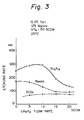
- Fig. 3 is a graph of the etching rates of Si3N4 SiO2 , and resist when the flow rate of CH2F2 is varied;
- Fig. 4 is a graph of the selectivities of etching of Si3N4 to SiO2 and resist when the flow rate of CH2F2 is varied.
- Figure 1 illustrates an anode coupling type dry etching apparatus.
- a reaction chamber 1 defined by a quartz tube 2
- An upper side electrode 4 is made of aluminum (Al) and anodized on its surface
- a lower side electrode 3 is made of aluminum on which a wafer 5 to be treated is placed.
- the lower side electrode 3 is connected to the ground 6, and the upper side electrode 4 is connected to a radio frequency (RF) source 7 of 13.56 MHz.
- RF radio frequency
- a matching network 8 is inserted between the upper side electrode 4 and the RF source 7.
- the reaction chamber 1 is evacuated by a vacuum pump (not shown).
- a silicon (Si) bulk or wafer 11 was prepared and a surface of the silicon bulk 11 was oxidized to form an SiO2 layer 12 of 30 nm thickness.
- An Si3N4 layer 13 was deposited onto the SiO2 layer 12 by sputtering, etc. The thickness of the Si3N4 layer 13 was 100 nm in this case, but could have also been made 150 nm.
- a resist layer 14 was coated on the Si3N4 layer 13 and patterned to leave a square or rectangular shape having a size L of 2.5 ⁇ m.
- a dry etching apparatus as in Fig. 1, the wafer 1 was placed on the lower side electrode 3.
- a radio frequency of 13.56 MHz was applied between the two electrodes 3 and 4 at a power of about 125 Watts.
- a portion of the Si3N4 layer 13 which was not covered with the patterned resist layer 14, was selectively etched or removed.
- the resist layer 14 was then removed.
- a patterned Si3N4 layer 13 was obtained on the SiO2 layer 12; the patterned Si3N4 layer 13 having a square or rectangular shape, as shown in Fig. 2B.
- oxidation was carried out in which the patterned Si3N4 layer 13 was used as a mask to locally oxidize the silicon bulk 11, that is, a portion of the silicon bulk 11 above which no Si3N4 layer exists was oxidized to form a thick SiO2 layer 15 or a locally oxidized silicon.
- "bird beaks" b were formed but had the width B of only 0.2 ⁇ m to 0.3 ⁇ m which was reduced from the width of the "bird beaks" in the prior art.
- the thickness of the SiO2 layer had to be 50 nm if the Si3N4 layer had a thickness of 100 nm. This resulted in a width of the "bird beaks" of 0.3 ⁇ m to 0.4 ⁇ m after patterning the Si3N4 layer and oxidizing the silicon bulk under the SiO2 layer using the Si3N4 layer as a mask.
- the thickness of an Si3N4 layer was made 150 nm while maintaining the thickness of an SiO2 layer at 30 nm. Successful selective etching of the Si3N4 layer could be done, that is, the SiO2 layer was not overetched, resulting in excellent local oxidation of a silicon bulk under the SiO2 layer.
- the flow rate of CH2F2 was varied with the other conditions being fixed.
- the fixed conditions of the test were vacuum of 33Pa (0.25 Torr), RF power of 125 Watts, flow rate of the SF6 of 50 SCCM, and temperature of 25°C.
- the etching rates of an Si3N4 layer, an SiO2 layer, and a resist layer were determined.
- the obtained etching rates and the selectivities of Si3N4 to SiO2 and resist or ratios of the etching rate of Si3N4 to SiO2 and resist, respectively, are summarized in the graphs in Figs. 3 and 4.
- a selectivity of etching of Si3N4 to SiO2 of more than 3, particularly, more than 4 was obtained in a process according to the present invention while at the highest only a selectivity of 2 to 3 could be obtained in a process in the prior art.
- a relatively high selectivity of etching of Si3N4/resist was obtained and is also preferable.
- a mixing ratio by volume or mole of CH2F2:SF6 of up to 35:100, more preferably 8 - 24:100, particularly 20:100, is preferably used in a process according to the present invention. This fact was ascertained in another test in which the flow-rate of SF6 is varied with the other conditions being fixed.
- a third test in which the degree of vacuum in a reaction chamber was varied and the other conditions were fixed was carried out.
Landscapes
- Drying Of Semiconductors (AREA)
Claims (12)
- Un procédé pour graver par voie sèche une couche de nitrure de silicium (13) par un gaz de gravure comprenant une combinaison d'hexafluorure de soufre et de fluorométhane.
- Un procédé selon la revendication 1, selon lequel ladite couche de nitrure de silicium (13) se trouve sur une couche de dioxyde de silicium (12) et une portion de ladite couche de nitrure de silicium est gravée sélectivement.
- Un procédé selon la revendication 1, selon lequel ledit fluorométhane est le difluorométhane.
- Un procédé selon la revendication 2, selon lequel ladite couche de dioxyde de silicium (12) a une épaisseur inférieure à 50 nm et ladite couche de nitrure de silicium (13) a une épaisseur de 100 nm à 200 nm.
- Un procédé selon la revendication 4, selon lequel ladite couche de dioxyde de silicium (12) a une épaisseur d'environ 30 nm et ladite couche de nitrure de silicium (13) a une épaisseur de 100 nm à 150 nm.
- Un procédé selon la revendication 1, selon lequel ladite gravure est conduite sous un vide de 13 Pa (0,1 Torr) ou plus.
- Un procédé selon la revendication 6, selon lequel ledit vide est de 27 à 40 Pa (0,2 Torr à 0,3 Torr).
- Un procédé selon la revendication 3, selon lequel le rapport d'alimentation entre l'hexafluorure de soufre et le difluorométhane, en volume, peut atteindre 35:100.
- Un procédé selon la revendication 4, selon lequel le rapport entre l'hexafluorure de soufre et le difluorométhane est de 8-24:100.
- Un procédé selon l'une quelconque des revendications 1 à 9, selon lequel ladite gravure par voie sèche est une gravure ionique.
- Un procédé selon la revendication 10, selon lequel ladite gravure ionique est conduite entre les électrodes (3, 4) du type à couplage d'anode.
- Un procédé pour former localement du silicium oxydé comprenant les étapes suivantes :préparation d'une pièce en silicium (11) ;oxydation d'une surface de la pièce en silicium (11) pour former une couche mince de dioxyde de silicium (12) sur la pièce en silicium (11) ;formation d'une couche de nitrure de silicium (13) sur la couche de dioxyde de silicium (12) ;formation d'une couche de matériau photorésistant (14) sur la couche de nitrure de silicium (13) ;formation d'un motif à la couche de matériau photorésistant (14) pour exposer une portion de la couche de nitrure de silicium (13) ;gravure par voie sèche sélective de ladite portion exposée en utilisant la couche (14) de matériau photorésistant portant un motif comme un masque, dans laquelle on utilise un gaz de gravure comprenant de l'hexafluorure de soufre et du fluorométhane ; etoxydation sélective d'une portion de la pièce en silicium (11) se trouvant sous la portion exposée de dioxyde de silicium (12) en utilisant la couche (13) de nitrure de silicium sélectivement gravée comme un masque, pour former une pièce en silicium localement oxydée.
Applications Claiming Priority (2)
| Application Number | Priority Date | Filing Date | Title |
|---|---|---|---|
| JP59280138A JPS61158143A (ja) | 1984-12-29 | 1984-12-29 | 窒化シリコン膜のエッチング方法 |
| JP280138/84 | 1984-12-29 |
Publications (3)
| Publication Number | Publication Date |
|---|---|
| EP0187601A2 EP0187601A2 (fr) | 1986-07-16 |
| EP0187601A3 EP0187601A3 (en) | 1988-03-16 |
| EP0187601B1 true EP0187601B1 (fr) | 1991-03-13 |
Family
ID=17620865
Family Applications (1)
| Application Number | Title | Priority Date | Filing Date |
|---|---|---|---|
| EP85402634A Expired - Lifetime EP0187601B1 (fr) | 1984-12-29 | 1985-12-26 | Procédé d'attaque sèche d'une couche de nitrure de silicium |
Country Status (4)
| Country | Link |
|---|---|
| EP (1) | EP0187601B1 (fr) |
| JP (1) | JPS61158143A (fr) |
| KR (1) | KR900006020B1 (fr) |
| DE (1) | DE3582146D1 (fr) |
Families Citing this family (2)
| Publication number | Priority date | Publication date | Assignee | Title |
|---|---|---|---|---|
| JP2720962B2 (ja) * | 1985-10-29 | 1998-03-04 | ソニー株式会社 | エツチングガス及びこれを用いたエツチング方法 |
| DE10135872A1 (de) * | 2001-07-24 | 2003-02-27 | Osram Opto Semiconductors Gmbh | Verfahren zur Herstellung einer Linse |
Family Cites Families (3)
| Publication number | Priority date | Publication date | Assignee | Title |
|---|---|---|---|---|
| NL8204437A (nl) * | 1982-11-16 | 1984-06-18 | Philips Nv | Werkwijze voor het vervaardigen van een halfgeleiderinrichting met behulp van plasma-etsen. |
| DE3420347A1 (de) * | 1983-06-01 | 1984-12-06 | Hitachi, Ltd., Tokio/Tokyo | Gas und verfahren zum selektiven aetzen von siliciumnitrid |
| JPH0612765B2 (ja) * | 1983-06-01 | 1994-02-16 | 株式会社日立製作所 | エ ッ チ ン グ 方 法 |
-
1984
- 1984-12-29 JP JP59280138A patent/JPS61158143A/ja active Granted
-
1985
- 1985-12-26 DE DE8585402634T patent/DE3582146D1/de not_active Expired - Lifetime
- 1985-12-26 EP EP85402634A patent/EP0187601B1/fr not_active Expired - Lifetime
- 1985-12-28 KR KR1019850010029A patent/KR900006020B1/ko not_active Expired
Also Published As
| Publication number | Publication date |
|---|---|
| DE3582146D1 (de) | 1991-04-18 |
| EP0187601A2 (fr) | 1986-07-16 |
| JPS61158143A (ja) | 1986-07-17 |
| JPH0426539B2 (fr) | 1992-05-07 |
| KR860005431A (ko) | 1986-07-23 |
| KR900006020B1 (ko) | 1990-08-20 |
| EP0187601A3 (en) | 1988-03-16 |
Similar Documents
| Publication | Publication Date | Title |
|---|---|---|
| US5013398A (en) | Anisotropic etch method for a sandwich structure | |
| US6015760A (en) | Method for enhancing oxide to nitride selectivity through the use of independent heat control | |
| US7541270B2 (en) | Methods for forming openings in doped silicon dioxide | |
| US8093155B2 (en) | Method of controlling striations and CD loss in contact oxide etch | |
| US5366590A (en) | Dry etching method | |
| EP0256311B1 (fr) | Procédé RIE pour graver des rainures d'isolation à parois verticales dans du silicium et du polycide | |
| US5286344A (en) | Process for selectively etching a layer of silicon dioxide on an underlying stop layer of silicon nitride | |
| US7273566B2 (en) | Gas compositions | |
| KR20010042983A (ko) | 고 종횡비 개구를 형성하는 방법 | |
| US6703315B2 (en) | Method of providing a shallow trench in a deep-trench device | |
| US4678539A (en) | Dry-etching method | |
| KR100311487B1 (ko) | 산화막식각방법 | |
| US6117788A (en) | Semiconductor etching methods | |
| US5180466A (en) | Process for dry etching a silicon nitride layer | |
| US6069087A (en) | Highly selective dry etching process | |
| US6653237B2 (en) | High resist-selectivity etch for silicon trench etch applications | |
| US5338395A (en) | Method for enhancing etch uniformity useful in etching submicron nitride features | |
| EP0187601A2 (fr) | Procédé d'attaque sèche d'une couche de nitrure de silicium | |
| KR20000061225A (ko) | 반도체소자의 트렌치 형성방법 | |
| KR100236078B1 (ko) | 반도체소자 식각방법 | |
| KR19990047250A (ko) | 반도체장치의 절연막 식각방법 |
Legal Events
| Date | Code | Title | Description |
|---|---|---|---|
| PUAI | Public reference made under article 153(3) epc to a published international application that has entered the european phase |
Free format text: ORIGINAL CODE: 0009012 |
|
| AK | Designated contracting states |
Kind code of ref document: A2 Designated state(s): DE FR GB |
|
| PUAL | Search report despatched |
Free format text: ORIGINAL CODE: 0009013 |
|
| AK | Designated contracting states |
Kind code of ref document: A3 Designated state(s): DE FR GB |
|
| 17P | Request for examination filed |
Effective date: 19880428 |
|
| 17Q | First examination report despatched |
Effective date: 19900420 |
|
| GRAA | (expected) grant |
Free format text: ORIGINAL CODE: 0009210 |
|
| AK | Designated contracting states |
Kind code of ref document: B1 Designated state(s): DE FR GB |
|
| REF | Corresponds to: |
Ref document number: 3582146 Country of ref document: DE Date of ref document: 19910418 |
|
| ET | Fr: translation filed | ||
| PLBE | No opposition filed within time limit |
Free format text: ORIGINAL CODE: 0009261 |
|
| STAA | Information on the status of an ep patent application or granted ep patent |
Free format text: STATUS: NO OPPOSITION FILED WITHIN TIME LIMIT |
|
| 26N | No opposition filed | ||
| PGFP | Annual fee paid to national office [announced via postgrant information from national office to epo] |
Ref country code: DE Payment date: 19930226 Year of fee payment: 8 |
|
| PG25 | Lapsed in a contracting state [announced via postgrant information from national office to epo] |
Ref country code: DE Effective date: 19940901 |
|
| PGFP | Annual fee paid to national office [announced via postgrant information from national office to epo] |
Ref country code: FR Payment date: 19951212 Year of fee payment: 11 |
|
| PGFP | Annual fee paid to national office [announced via postgrant information from national office to epo] |
Ref country code: GB Payment date: 19951218 Year of fee payment: 11 |
|
| PG25 | Lapsed in a contracting state [announced via postgrant information from national office to epo] |
Ref country code: GB Effective date: 19961226 |
|
| GBPC | Gb: european patent ceased through non-payment of renewal fee |
Effective date: 19961226 |
|
| PG25 | Lapsed in a contracting state [announced via postgrant information from national office to epo] |
Ref country code: FR Effective date: 19970829 |
|
| REG | Reference to a national code |
Ref country code: FR Ref legal event code: ST |