EP0187668A2 - Capteur d'ultrasons et sa méthode de fabrication - Google Patents
Capteur d'ultrasons et sa méthode de fabrication Download PDFInfo
- Publication number
- EP0187668A2 EP0187668A2 EP86100194A EP86100194A EP0187668A2 EP 0187668 A2 EP0187668 A2 EP 0187668A2 EP 86100194 A EP86100194 A EP 86100194A EP 86100194 A EP86100194 A EP 86100194A EP 0187668 A2 EP0187668 A2 EP 0187668A2
- Authority
- EP
- European Patent Office
- Prior art keywords
- electrode
- unpolarized
- polarized
- electrodes
- conductive lead
- Prior art date
- Legal status (The legal status is an assumption and is not a legal conclusion. Google has not performed a legal analysis and makes no representation as to the accuracy of the status listed.)
- Granted
Links
Images


Classifications
-
- H—ELECTRICITY
- H10—SEMICONDUCTOR DEVICES; ELECTRIC SOLID-STATE DEVICES NOT OTHERWISE PROVIDED FOR
- H10N—ELECTRIC SOLID-STATE DEVICES NOT OTHERWISE PROVIDED FOR
- H10N30/00—Piezoelectric or electrostrictive devices
- H10N30/01—Manufacture or treatment
- H10N30/09—Forming piezoelectric or electrostrictive materials
- H10N30/098—Forming organic materials
-
- B—PERFORMING OPERATIONS; TRANSPORTING
- B06—GENERATING OR TRANSMITTING MECHANICAL VIBRATIONS IN GENERAL
- B06B—METHODS OR APPARATUS FOR GENERATING OR TRANSMITTING MECHANICAL VIBRATIONS OF INFRASONIC, SONIC, OR ULTRASONIC FREQUENCY, e.g. FOR PERFORMING MECHANICAL WORK IN GENERAL
- B06B1/00—Methods or apparatus for generating mechanical vibrations of infrasonic, sonic, or ultrasonic frequency
- B06B1/02—Methods or apparatus for generating mechanical vibrations of infrasonic, sonic, or ultrasonic frequency making use of electrical energy
- B06B1/06—Methods or apparatus for generating mechanical vibrations of infrasonic, sonic, or ultrasonic frequency making use of electrical energy operating with piezoelectric effect or with electrostriction
- B06B1/0607—Methods or apparatus for generating mechanical vibrations of infrasonic, sonic, or ultrasonic frequency making use of electrical energy operating with piezoelectric effect or with electrostriction using multiple elements
- B06B1/0622—Methods or apparatus for generating mechanical vibrations of infrasonic, sonic, or ultrasonic frequency making use of electrical energy operating with piezoelectric effect or with electrostriction using multiple elements on one surface
-
- H—ELECTRICITY
- H10—SEMICONDUCTOR DEVICES; ELECTRIC SOLID-STATE DEVICES NOT OTHERWISE PROVIDED FOR
- H10N—ELECTRIC SOLID-STATE DEVICES NOT OTHERWISE PROVIDED FOR
- H10N30/00—Piezoelectric or electrostrictive devices
- H10N30/01—Manufacture or treatment
- H10N30/04—Treatments to modify a piezoelectric or electrostrictive property, e.g. polarisation characteristics, vibration characteristics or mode tuning
- H10N30/045—Treatments to modify a piezoelectric or electrostrictive property, e.g. polarisation characteristics, vibration characteristics or mode tuning by polarising
-
- Y—GENERAL TAGGING OF NEW TECHNOLOGICAL DEVELOPMENTS; GENERAL TAGGING OF CROSS-SECTIONAL TECHNOLOGIES SPANNING OVER SEVERAL SECTIONS OF THE IPC; TECHNICAL SUBJECTS COVERED BY FORMER USPC CROSS-REFERENCE ART COLLECTIONS [XRACs] AND DIGESTS
- Y10—TECHNICAL SUBJECTS COVERED BY FORMER USPC
- Y10S—TECHNICAL SUBJECTS COVERED BY FORMER USPC CROSS-REFERENCE ART COLLECTIONS [XRACs] AND DIGESTS
- Y10S310/00—Electrical generator or motor structure
- Y10S310/80—Piezoelectric polymers, e.g. PVDF
-
- Y—GENERAL TAGGING OF NEW TECHNOLOGICAL DEVELOPMENTS; GENERAL TAGGING OF CROSS-SECTIONAL TECHNOLOGIES SPANNING OVER SEVERAL SECTIONS OF THE IPC; TECHNICAL SUBJECTS COVERED BY FORMER USPC CROSS-REFERENCE ART COLLECTIONS [XRACs] AND DIGESTS
- Y10—TECHNICAL SUBJECTS COVERED BY FORMER USPC
- Y10T—TECHNICAL SUBJECTS COVERED BY FORMER US CLASSIFICATION
- Y10T29/00—Metal working
- Y10T29/42—Piezoelectric device making
Definitions
- This invention relates to an ultrasonic transducer and to a method of manufacturing the same.
- Ultrasonic transducers are widely employed as the probes in ultrasound diagnostic equipment for real-time observation of the tomograph of a living body, in ultrasound materials testing equipment for the non-destructive testing of materials, and in many other applications.
- a piezoelectric polymer material such as polyvinylidene fluoride (PVDF) or a composite of a ferro-electric ceramic powder and a polymer.
- PVDF polyvinylidene fluoride
- a piezoelectric polymer material exhibits excellent acoustic matching with respect to a living body since its acoustic impedence is closer to that of a living body than is the acoustic impedence of conventional ceramic materials.
- Such a piezoelectric polymer material also has a low mechanical Q, as a result of which improved sensitivity and response are anticipated, and exhibits flexibility that enables the vibrator to be machined into almost any shape with comparative ease.
- Another reason for using a piezoelectric polymer material is its high anisotropy. Specifically, the vibrating efficiency of such a material in the direction of its thickness is considerably higher than in a direction perpendicular thereto, namely the transverse direction, so that the material can be formed into a vibrator approximating an ideal piston acoustic source. Since the thickness of such a vibrator can be made very small, application in the high-frequency region is widespread.
- the array pattern electrodes are formed by a technique such as photoetching, screen printing or vapor deposition.
- a technique such as photoetching, screen printing or vapor deposition.
- the array element spacing is further reduced for the purpose of minimizing the grating lobe, it is sometimes difficult to form array pattern electrodes which are stable in terms of shape by using the foregoing method. This can lead to a deterioration in acoustic characteristics.
- a first object of the present invention is to provide an ultrasonic transducer having excellent acoustic characteristics in the high-frequency region with use of a piezoelectric polymer material.
- a second object of the present invention is to provide a method of manufacturing such an ultrasonic transducer.
- the first object is attained by providing an ultrasonic transducer comprising: a plate-shaped piezoelectric body consisting of a piezoelectric polymer material and having a polarized portion obtained by polarizing a prescribed region thereof, an unpolarized portion contiguous to the polarized portion, and opposing first and second main surfaces; a first electrode formed on the first main surface of the piezoelectric body to cover the polarized portion and having an edge portion extending over the unpolarized portion; a second electrode formed on the second main surface of the piezoelectric body to cover the polarized portion and having an edge portion extending over the unpolarized portion; a first conductive lead electrically connected to the edge portion of the first electrode; and a second conductive lead electrically connected to the edge portion of the second electrode.
- the first electrode comprises a plurality of electrodes arranged in a side-by-side array having a prescribed inter-electrode spacing
- the first conductive lead comprises a plurality of conductors the number whereof is identical with the number of electrodes constituting the first electrode
- the second electrode comprises a single common electrode opposing the first electrode.
- the unpolarized portion of the piezoelectric body has first and second regions situated on a plane different from that of the polarized portion, and the edge portions of the first and second electrodes are situated on the first and second regions, respectively.
- the second object is attained by providing a method of manufacturing an ultrasonic transducer comprising steps of: forming a polarized portion and an unpolarized portion at prescribed regions of a plate-shaped piezoelectric body consisting of a piezoelectric polymer material having opposing first and second main surfaces by bringing first and second electrical conductors into intimate contact with the first and second main surfaces, respectively, and applying a voltage at least across the first and second electrical conductors; depositing a first electrode on the first main surface to cover the polarized portion and to extend over a region of the unpolarized portion, and a second electrode on the second main surface to cover the polarized portion and to extend over a region of the unpolarized portion, the first and second electrodes each comprising an electrical conductor; depositing first and second electrically conductive leads on a main surface of a flexible substrate; bonding an end portion of the first electrically conductive lead to the first electrode at an edge portion thereof extended over the region of the unpolarized portion, and an end portion of
- the second object may also be attained by providing a method of manufacturing an ultrasonic transducer comprising steps of: forming a polarized portion and an unpolarized portion at prescribed regions of a plate-shaped piezoelectric body consisting of a piezoelectric polymer material having opposing first and second main surfaces by bringing first and second electrical conductors into intimate contact with the first and second main surfaces, respectively, and applying a voltage at least across the first and second electrical conductors; depositing a first electrode on the first main surface to cover the polarized portion and to extend over the region of the unpolarized portion, and a second electrode on the second main surface to cover the polarized portion and to extend over the region of the unpolarized portion, the first and second electrodes each comprising an electrical conductor; depositing first and second electrically conductive leads on a main surface of a flexible substrate, the first electrically conductive lead each consisting of a plurality of electrically conductive patterns connected commonly at first end thereof and having second end branching outwardly from the
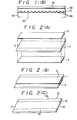
- Figs. 2(A) - 2(C) illustrate a procedure in which a piezoelectric polymer material is used to form a piezoelectric body (or member) a prescribed region of which has a polarized portion.
- the piezoelectric polymer material consists of polyvinyl fluoride, polyvinylidene fluoride, vinylidene fluoride - vinyl fluoride copolymer, vinylidene fluoride - ethylene trifluoride copolymer, vinylidene fluoride - ethylene tetrafluoride copolymer, vinylidene cyanide - vinyl acetate copolymer, vinylidene cyanide - acrylnitrile copolymer, vinylidene cyanide - vinylidene chloride copolymer, vinylidene cyanide - styrene copolymer, vinylidene cyanide - methyl methacrylate copolymer, vinylidene cyanide
- the piezoelectric polymer material may also consist of a composite obtained by kneading finely divided powder of a ferro-electric ceramic such as lead titanate or lead zirconate titanate with a polymeric material such as polyvinylidene fluoride, polyvinyl fluoride, nylon, polyacetal or polyacrylnitrile.
- a ferro-electric ceramic such as lead titanate or lead zirconate titanate
- a polymeric material such as polyvinylidene fluoride, polyvinyl fluoride, nylon, polyacetal or polyacrylnitrile.
- a polymeric piezoelectric member 1 has a prescribed region 2 which is to be subjected to a polarization treatment. Electrically conductive plates 3, 4 made of copper or the like and shaped to correspond to the region 2 are brought into intimate abutting contact with the upper and lower main surfaces, respectively, of the piezoelectric member 1 so as to cover the region 2, as shown in Fig. 2(B). The prescribed region 2 of the piezoelectric member 1 is then polarized by applying a voltage across the conductive plates 3, 4, after which the plates 3, 4 are removed.
- the temperature range is 10 to 180°C, preferably 40 to 175°C
- the electric field strength ranges from 50 kV/cm up to the dielectric breakdown strength, preferably 100 to 2000 kV/cm
- the voltage is applied from 10 sec to 10 hr, preferably from 10 min to 2 hr.
- a piezoelectric body 11 having a polarized portion 12 located at the central portion of the piezoelectric body and extending along its minor axis, as well as an unpolarized portion 13 along each longitudinal side edge of the piezoelectric body:
- Figs. 3(A) - 3(D) are views illustrating a procedure for forming electrodes on the partially polarized piezoelectric body 11.
- Fig. 3(A) depicts the piezoelectric body 11 having the polarized portion 12 formed as described above.
- an electrically conductive material for forming first and second electrodes 14, 15 is deposited on the first [Fig. 3(B)] and second [Fig. 3(C)] main surfaces, respectively, of the piezoelectric body 11 by a known method such as vacuum deposition, sputtering or screen printing.
- the first electrode 14 is formed on the first main surface to cover only one of the unpolarized portions 13, leaving the other unpolarized portion 13 exposed, as indicated at numeral 13a.
- the second electrode 15 is formed on the second main surface to cover only the unpolarized portion 13 thereof corresponding to the exposed unpolarized portion 13a.
- the unpolarized portion 13 left exposed is indicated at numeral 13b.
- the resulting piezoelectric body 11 has the unpolarized portions 13 on both sides of the polarized portion 12 and contiguous thereto, the main portion of the first electrode 14 located on that portion of the first main surface corresponding to the polarized portion 12, the second electrode 15 located on that portion of the second main surface corresponding to the polarized portion 12, a connective edge portion 14a of the first electrode 14 extending over the unpolarized portion 13b on the first main surface, and a connective edge portion 15a of the second electrode 15 extending over the unpolarized portion 13a on the second main surface.
- an acoustic matching layer 16 is so deposited on the second surface of the piezoelectric body 11 having the second electrode 15 as to cover the region constituted by the polarized portion 12.
- the acoustic matching layer 16 also functions to protect the acoustic radiation surface of the piezoelectric body 11 including the second electrode 15 and consists of a flexible film of polyester or polyimide of low acoustic impedence deposited on the second surface by bonding or, preferably, by thermal fusion.
- a substrate 20 comprising a flexible insulator such as polyimide or polyester is formed to include an opening 21.
- the width of the opening 21 is equivalent to that of the piezoelectric body 11 minus the connective edge portions 14a, 15a, and its length is approximately the same as that of the piezoelectric body 11 along the major axis thereof.
- first and second conductive lead edge portions 22, 23 are arranged on the surface of substrate 20 in contact with the longitudinal side edges of the opening 21 corresponding to the connective edge portions 14a, 15a and of the same width.
- a plurality of first conductive leads 24 extend along the surface of the substrate 20 from the conductive lead edge portion 22 to one side edge of the substrate 20, and a pair of second conductive leads 25 extend along the surface of the substrate 20 from the conductive lead edge portion 22 to the side edge of the substrate 20.
- the distal end portions of the leads 24, 25 form terminal portions 26, 27, 28 at the side edge of the substrate 20 so that a connection can be made to external circuitry, not shown.
- These conductive lead patterns are formed by being deposited using a method such a vapor deposition or photoetching.
- the number of conductive lead patterns constituting the first conductive leads 24 is equal to the number of elements in the array.
- Fig. 5(B) is a view illustrating the manner in which the piezoelectric body 11 including the electrodes 14, 15 has been inserted into the opening 21.
- the leads 24 and 25 are extended on the same surface of the substrate 20, while the electrodes 14 and 15 are deposited on the opposing surfaces of the piezoelectric body 11 respectively.
- the conductive lead edge portion 22 which is to be bonded to the connective edge portion 14a, is extended beyond over the edge 40 of the substrate 20, in advance.
- the leads 24, 25 are deposited on opposing surfaces of the substrate 20, respectively, it is not necessary for the conductive lead edge portion 22 to be extended over the edge 40.
- the piezoelectric body 11 is inserted into the opening 21 of substrate 20, and the edge portions 14a, 15a of the first and second electrodes 14, 15 are respectively bonded to the first and second conductive lead edge portions 22, 23 via adhesive layers 30, 31 consisting of an electrically conductive adhesive.
- Fig. 6(B) is an enlarged view of the bonded portions.
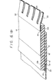
- the first electrode 14 is divided into a plurality of electrodes constituting an electrode array. This is accomplished, as shown in Fig. 7, by using a dicing saw or the like to simultaneously cut the conductive lead edge portion 22 and first electrode 14 into segments coinciding with respective ones of the conductive leads 24 formed on the substrate 20 at locations corresponding to the array elements.
- the cutting operation forms grooves 32 only so deep as to reach the bottom surface of the first electrode 14.
- the first electrode 14 is partitioned into an array of plural electrodes 14b arranged side by side with a very small inter-electrode spacing, and each electrode 14b is reliably connected to its corresponding conductive lead 24.
- the result is a plurality of array elements 33.
- the piezoelectric element so obtained comprises the array elements 33 formed and arranged in a highly precise manner.
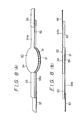
- the piezoelectric element of Fig. 7 is bonded to a backing 40, which consists of a material such as epoxy resin, to form a linear array transducer.
- the piezoelectric transducer is bonded to the backing 40 in such a manner that the polarized portion 12 is disposed on the upper edge surface of the backing, with the surface of the polarized portion having the second electrode 15 deposited thereon being faced upward.
- the piezoelectric body 11 and substrate 20 are bent and then bonded to the backing 40 in such a manner that the joints between the first and second electrode edge portions 14a, 15a and the first and second conductive lead edge portions 22, 23, respectively, are positioned at the sides of the backing 40.
- numeral 41 denotes a case
- 42 represents an effective acoustic radiation surface.
- the junctions between the electrodes 14, 15 and the conductive leads 24, 25 are situated on the unpolarized portions 13a, 13b, and the junctions 43, 44 are situated on the sides of the backing 40 remote from the acoustic radiation surface 42.
- Such an arrangement eliminates the adverse influence of the junctions 43, 44, which act as unnecessary acoustic interfaces.
- the upper end face of the backing 40d is recessed by exploiting the flexibility of the piezoelectric body 11. This has the effect of focusing sound waves in a direction perpendicular to the ultrasonic scanning direction.
- the ultrasonic transducer having the foregoing construction can be formed in a very simple manner.
- the method of the invention includes polarizing solely the prescribed region of the piezoelectric polymer member, subsequently depositing the first and second electrodes which correspond to the common electrode and array electrodes covering the polarized portion and having edge portions situated at the unpolarized portions, thereafter connecting these first and second electrode edge portions to the conductive lead edge portions formed on the flexible substrate, and then cutting the first electrode and the corresponding conductive lead edge portion simultaneously by a dicing saw to form array electrodes, a highly dense array of elements can be formed with great precision and stability. The result is a high-density array-type ultrasonic transducer particularly well-suited for application in the high-frequency region.
- the piezoelectric member since the array electrodes of the piezoelectric member are formed and the array electrodes are essentially electrically connected to external circuitry all through a simple process of manufacture, the overall process is curtailed. In addition, since the piezoelectric member is cut only to the depth of the array electrode portion, the piezoelectric material exhibits a high mechanical strength. The result is a stable ultrasonic transducer having a high degree of strength where the piezoelectric body is bonded to the acoustic matching layer and backing.
- the transducer Since the overall piezoelectric element exhibits flexibility, it can be freely deformed into a desired configuration.
- the transducer is applicable not only to linear array probes but can be converted into probes of the arc array and convex array type. Accordingly, the ultrasonic transducer can be widely applied to various methods of ultrasound tomography and to the diagnosis of various regions of a living body.
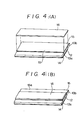
- a piezoelectric body 50 comprising a piezoelectric polymer member has a disk-shaped polarized portion 51 and linear unpolarized portions 52, 53 extending from the periphery of the polarized portion 51.
- a first electrode 54 is deposited on the polarized portion 51 and unpolarized portion 52 so as to cover their upper surface.
- a second electrode 55 is deposited on the polarized portion 51 and unpolarized portion 53 so as to cover their lower surface.
- the first electrode 54 has an end portion 54a situated at the end of the unpolarized portion 52, and the second electrode 55 has an end portion 55a situated at the end of the unpolarized portion 53.
- First and second conductive leads 56, 57 are formed so as to be connected to the first and second electrode end portions 54a, 55a, respectively. The effects obtained are similar to those of the embodiment of Fig. 1.
- the junctions between the electrodes and the conductive leads are situated on the unpolarized portions, and the junctions are situated at locations remote from the acoustic radiation surface.
- the junctions which act as unnecessary acoustic interfaces, have no adverse influence upon the effective acoustic radiation surface so that the acoustic characteristics in the high-frequency region can be improved.
- the method of manufacture of the present invention includes polarizing solely the prescribed region of the piezoelectric polymer member, subsequently depositing the first and second electrodes covering the polarized portion and having edge portions situated on the unpolarized portions, thereafter connecting these first and second electrode edge portions to the conductive lead edge portions formed on the flexible substrate, and then cutting the first electrode and the junction between the first electrode and conductive lead portion at the same time to form array electrodes. Accordingly, the manufacturing method of the present invention makes it possible to form a highly dense array of elements with great precision and stability.
Landscapes
- Engineering & Computer Science (AREA)
- Mechanical Engineering (AREA)
- Manufacturing & Machinery (AREA)
- Transducers For Ultrasonic Waves (AREA)
- Ultra Sonic Daignosis Equipment (AREA)
- Piezo-Electric Transducers For Audible Bands (AREA)
- Investigating Or Analyzing Materials By The Use Of Ultrasonic Waves (AREA)
Applications Claiming Priority (2)
| Application Number | Priority Date | Filing Date | Title |
|---|---|---|---|
| JP1402/85 | 1985-01-10 | ||
| JP60001402A JPS61161446A (ja) | 1985-01-10 | 1985-01-10 | 超音波探触子およびその製造方法 |
Publications (3)
| Publication Number | Publication Date |
|---|---|
| EP0187668A2 true EP0187668A2 (fr) | 1986-07-16 |
| EP0187668A3 EP0187668A3 (en) | 1989-01-25 |
| EP0187668B1 EP0187668B1 (fr) | 1993-04-28 |
Family
ID=11500497
Family Applications (1)
| Application Number | Title | Priority Date | Filing Date |
|---|---|---|---|
| EP86100194A Expired - Lifetime EP0187668B1 (fr) | 1985-01-10 | 1986-01-08 | Capteur d'ultrasons et sa méthode de fabrication |
Country Status (4)
| Country | Link |
|---|---|
| US (1) | US4704774A (fr) |
| EP (1) | EP0187668B1 (fr) |
| JP (1) | JPS61161446A (fr) |
| DE (1) | DE3688335T2 (fr) |
Cited By (1)
| Publication number | Priority date | Publication date | Assignee | Title |
|---|---|---|---|---|
| FR2700220A1 (fr) * | 1993-01-06 | 1994-07-08 | Saint Louis Inst | Procédé pour polariser au moins une zone d'une feuille de matériau ferroélectrique, et procédé pour réaliser un élément polarisé pour capteur piézoélectrique ou pyroélectrique. |
Families Citing this family (25)
| Publication number | Priority date | Publication date | Assignee | Title |
|---|---|---|---|---|
| DE3650004T2 (de) * | 1985-05-20 | 1995-02-23 | Matsushita Electric Ind Co Ltd | Ultraschallsonde. |
| US4977655A (en) * | 1986-04-25 | 1990-12-18 | Intra-Sonix, Inc. | Method of making a transducer |
| JP2545861B2 (ja) * | 1987-06-12 | 1996-10-23 | 富士通株式会社 | 超音波探触子の製造方法 |
| DE3883638T2 (de) * | 1987-06-27 | 1994-04-21 | Shimadzu Corp | Flexibles Replika-Gitter und optischer Multiplexer/Demultiplexer mit Anwendung eines solchen Gitters. |
| NZ243294A (en) * | 1991-06-25 | 1995-04-27 | Commw Scient Ind Res Org | Time of flight of acoustic wave packets through fluid: reduction of higher order acoustic mode effects |
| US5295487A (en) * | 1992-02-12 | 1994-03-22 | Kabushiki Kaisha Toshiba | Ultrasonic probe |
| US5453575A (en) * | 1993-02-01 | 1995-09-26 | Endosonics Corporation | Apparatus and method for detecting blood flow in intravascular ultrasonic imaging |
| US5608692A (en) * | 1994-02-08 | 1997-03-04 | The Whitaker Corporation | Multi-layer polymer electroacoustic transducer assembly |
| DE69516444T2 (de) * | 1994-03-11 | 2001-01-04 | Intravascular Research Ltd., London | Ultraschall Wandleranordnung und Verfahren zu dessen Herstellung |
| US7226417B1 (en) | 1995-12-26 | 2007-06-05 | Volcano Corporation | High resolution intravascular ultrasound transducer assembly having a flexible substrate |
| US5857974A (en) | 1997-01-08 | 1999-01-12 | Endosonics Corporation | High resolution intravascular ultrasound transducer assembly having a flexible substrate |
| US6113546A (en) | 1998-07-31 | 2000-09-05 | Scimed Life Systems, Inc. | Off-aperture electrical connection for ultrasonic transducer |
| US6406433B1 (en) * | 1999-07-21 | 2002-06-18 | Scimed Life Systems, Inc. | Off-aperture electrical connect transducer and methods of making |
| CA2332158C (fr) * | 2000-03-07 | 2004-09-14 | Matsushita Electric Industrial Co., Ltd. | Sonde ultrasonique |
| US6723052B2 (en) * | 2001-06-07 | 2004-04-20 | Stanley L. Mills | Echogenic medical device |
| JP2003158794A (ja) * | 2001-11-20 | 2003-05-30 | Taiyo Yuden Co Ltd | 圧電音響装置 |
| EP1619925B1 (fr) * | 2003-04-01 | 2017-11-01 | Olympus Corporation | Vibrateur ultrasonore et son procede de fabrication |
| JP4469928B2 (ja) * | 2004-09-22 | 2010-06-02 | ベックマン・コールター・インコーポレーテッド | 攪拌容器 |
| JP4351229B2 (ja) | 2006-06-28 | 2009-10-28 | ジーイー・メディカル・システムズ・グローバル・テクノロジー・カンパニー・エルエルシー | 超音波探触子の製造方法 |
| JP4900066B2 (ja) * | 2007-06-12 | 2012-03-21 | ミツミ電機株式会社 | 超音波センサの製造方法 |
| US8531178B2 (en) | 2007-11-26 | 2013-09-10 | Konica Minolta Medical & Graphic, Inc. | Ultrasound probe, method for manufacturing the same, and ultrasound diagnostic apparatus |
| JP5243311B2 (ja) * | 2009-03-09 | 2013-07-24 | ジーイー・メディカル・システムズ・グローバル・テクノロジー・カンパニー・エルエルシー | フレキシブルプリント基板、超音波探触子および超音波探触子の製造方法 |
| US11225961B2 (en) * | 2017-02-21 | 2022-01-18 | Sensus Spectrum, Llc | Multi-element bending transducers and related methods and devices |
| US11504546B2 (en) | 2019-02-28 | 2022-11-22 | Cowles Ventures, Llc | Needle guidance device for brachytherapy and method of use |
| US11524176B2 (en) | 2019-03-14 | 2022-12-13 | Cowles Ventures, Llc | Locator for placement of fiducial support device method |
Family Cites Families (10)
| Publication number | Priority date | Publication date | Assignee | Title |
|---|---|---|---|---|
| US3365593A (en) * | 1965-10-21 | 1968-01-23 | Phillips Petroleum Co | Piezoelectric transducers |
| CA1026237A (fr) * | 1973-09-17 | 1978-02-14 | Kureha Kagaku Kogyo Kabushiki Kaisha | Commutateur de clavier |
| JPS5410214B2 (fr) * | 1973-10-15 | 1979-05-02 | ||
| JPS51129129A (en) * | 1975-05-02 | 1976-11-10 | Kureha Chem Ind Co Ltd | Matrix switch |
| AT375466B (de) * | 1977-07-27 | 1984-08-10 | List Hans | Messwertaufnehmer mit einem piezoelektrischen messelement |
| JPS5840805B2 (ja) * | 1978-04-10 | 1983-09-08 | 東レ株式会社 | 座標入力用構造体 |
| JPS55151892A (en) * | 1979-05-16 | 1980-11-26 | Toray Ind Inc | Electrode division type transducer using high molecular piezoelectric film |
| DE3069001D1 (en) * | 1979-05-16 | 1984-09-27 | Toray Industries | Piezoelectric vibration transducer |
| US4315433A (en) * | 1980-03-19 | 1982-02-16 | The United States Of America As Represented By The Secretary Of The Army | Polymer film accelerometer |
| US4433400A (en) * | 1980-11-24 | 1984-02-21 | The United States Of America As Represented By The Department Of Health And Human Services | Acoustically transparent hydrophone probe |
-
1985
- 1985-01-10 JP JP60001402A patent/JPS61161446A/ja active Pending
-
1986
- 1986-01-08 DE DE8686100194T patent/DE3688335T2/de not_active Expired - Fee Related
- 1986-01-08 EP EP86100194A patent/EP0187668B1/fr not_active Expired - Lifetime
-
1987
- 1987-03-31 US US07/032,750 patent/US4704774A/en not_active Expired - Fee Related
Cited By (2)
| Publication number | Priority date | Publication date | Assignee | Title |
|---|---|---|---|---|
| FR2700220A1 (fr) * | 1993-01-06 | 1994-07-08 | Saint Louis Inst | Procédé pour polariser au moins une zone d'une feuille de matériau ferroélectrique, et procédé pour réaliser un élément polarisé pour capteur piézoélectrique ou pyroélectrique. |
| US5491879A (en) * | 1993-01-06 | 1996-02-20 | Institut Franco-Allemand De Recherches De Saint-Louis | Procedure to polarize at least one zone of a foil of ferroelectric material to produce a polarized element for piezoelectric or pyroelectric transducers |
Also Published As
| Publication number | Publication date |
|---|---|
| US4704774A (en) | 1987-11-10 |
| DE3688335T2 (de) | 1993-09-23 |
| DE3688335D1 (de) | 1993-06-03 |
| EP0187668B1 (fr) | 1993-04-28 |
| EP0187668A3 (en) | 1989-01-25 |
| JPS61161446A (ja) | 1986-07-22 |
Similar Documents
| Publication | Publication Date | Title |
|---|---|---|
| US4704774A (en) | Ultrasonic transducer and method of manufacturing same | |
| EP0176030B1 (fr) | Transducteur ultrasonore et procédé de sa fabrication | |
| EP0210723B1 (fr) | Transducteur ultrason | |
| US5704105A (en) | Method of manufacturing multilayer array ultrasonic transducers | |
| EP0167740B1 (fr) | Transducteur ultrasonore avec un film polymère piézoélectrique multiplié | |
| US5640370A (en) | Two-dimensional acoustic array and method for the manufacture thereof | |
| US4425525A (en) | Ultrasonic transducer array shading | |
| JPS61144565A (ja) | 高分子圧電型超音波探触子 | |
| US6558332B1 (en) | Array type ultrasonic probe and a method of manufacturing the same | |
| US6333590B1 (en) | Ultrasonic transducer having laminate structure, ultrasonic probe and production method thereof | |
| JPH0683516B2 (ja) | 超音波探触子およびその製造方法 | |
| JP2024141458A (ja) | 超音波探触子 | |
| JPH023599B2 (fr) | ||
| JPS6181000A (ja) | 積層高分子圧電型超音波探触子 | |
| JPS6222634A (ja) | 超音波探触子 | |
| JPS6178300A (ja) | 超音波探触子およびその製造方法 | |
| JPH01166699A (ja) | 複合圧電板の製造方法 | |
| JPS5997299A (ja) | 超音波探触子 | |
| JPS6269800A (ja) | 高分子圧電型超音波探触子 | |
| JPS61294998A (ja) | 高分子圧電型超音波探触子 | |
| JP2638775B2 (ja) | 超音波探触子の製造方法 | |
| JPS63175761A (ja) | 超音波探触子 | |
| JP2935550B2 (ja) | 超音波探触子 | |
| JPH07274292A (ja) | 配列型の超音波探触子 | |
| JPH0323209Y2 (fr) |
Legal Events
| Date | Code | Title | Description |
|---|---|---|---|
| PUAI | Public reference made under article 153(3) epc to a published international application that has entered the european phase |
Free format text: ORIGINAL CODE: 0009012 |
|
| 17P | Request for examination filed |
Effective date: 19860205 |
|
| AK | Designated contracting states |
Kind code of ref document: A2 Designated state(s): BE DE FR GB NL |
|
| PUAL | Search report despatched |
Free format text: ORIGINAL CODE: 0009013 |
|
| RHK1 | Main classification (correction) |
Ipc: G10K 11/34 |
|
| AK | Designated contracting states |
Kind code of ref document: A3 Designated state(s): BE DE FR GB NL |
|
| 17Q | First examination report despatched |
Effective date: 19910619 |
|
| RBV | Designated contracting states (corrected) |
Designated state(s): DE FR |
|
| GRAA | (expected) grant |
Free format text: ORIGINAL CODE: 0009210 |
|
| AK | Designated contracting states |
Kind code of ref document: B1 Designated state(s): DE FR |
|
| REF | Corresponds to: |
Ref document number: 3688335 Country of ref document: DE Date of ref document: 19930603 |
|
| ET | Fr: translation filed | ||
| PLBE | No opposition filed within time limit |
Free format text: ORIGINAL CODE: 0009261 |
|
| STAA | Information on the status of an ep patent application or granted ep patent |
Free format text: STATUS: NO OPPOSITION FILED WITHIN TIME LIMIT |
|
| 26N | No opposition filed | ||
| PGFP | Annual fee paid to national office [announced via postgrant information from national office to epo] |
Ref country code: FR Payment date: 20020110 Year of fee payment: 17 |
|
| PGFP | Annual fee paid to national office [announced via postgrant information from national office to epo] |
Ref country code: DE Payment date: 20020212 Year of fee payment: 17 |
|
| PG25 | Lapsed in a contracting state [announced via postgrant information from national office to epo] |
Ref country code: DE Free format text: LAPSE BECAUSE OF NON-PAYMENT OF DUE FEES Effective date: 20030801 |
|
| PG25 | Lapsed in a contracting state [announced via postgrant information from national office to epo] |
Ref country code: FR Free format text: LAPSE BECAUSE OF NON-PAYMENT OF DUE FEES Effective date: 20030930 |
|
| REG | Reference to a national code |
Ref country code: FR Ref legal event code: ST |