EP0187706B1 - Verfahren zur Metallbeschichtung eines organischen Substrates - Google Patents
Verfahren zur Metallbeschichtung eines organischen Substrates Download PDFInfo
- Publication number
- EP0187706B1 EP0187706B1 EP86300070A EP86300070A EP0187706B1 EP 0187706 B1 EP0187706 B1 EP 0187706B1 EP 86300070 A EP86300070 A EP 86300070A EP 86300070 A EP86300070 A EP 86300070A EP 0187706 B1 EP0187706 B1 EP 0187706B1
- Authority
- EP
- European Patent Office
- Prior art keywords
- substrate
- metal
- temperature
- polyimide
- copper
- Prior art date
- Legal status (The legal status is an assumption and is not a legal conclusion. Google has not performed a legal analysis and makes no representation as to the accuracy of the status listed.)
- Expired
Links
Images


Classifications
-
- H—ELECTRICITY
- H10—SEMICONDUCTOR DEVICES; ELECTRIC SOLID-STATE DEVICES NOT OTHERWISE PROVIDED FOR
- H10W—GENERIC PACKAGES, INTERCONNECTIONS, CONNECTORS OR OTHER CONSTRUCTIONAL DETAILS OF DEVICES COVERED BY CLASS H10
- H10W70/00—Package substrates; Interposers; Redistribution layers [RDL]
- H10W70/60—Insulating or insulated package substrates; Interposers; Redistribution layers
- H10W70/67—Insulating or insulated package substrates; Interposers; Redistribution layers characterised by their insulating layers or insulating parts
- H10W70/69—Insulating materials thereof
- H10W70/695—Organic materials
-
- C—CHEMISTRY; METALLURGY
- C23—COATING METALLIC MATERIAL; COATING MATERIAL WITH METALLIC MATERIAL; CHEMICAL SURFACE TREATMENT; DIFFUSION TREATMENT OF METALLIC MATERIAL; COATING BY VACUUM EVAPORATION, BY SPUTTERING, BY ION IMPLANTATION OR BY CHEMICAL VAPOUR DEPOSITION, IN GENERAL; INHIBITING CORROSION OF METALLIC MATERIAL OR INCRUSTATION IN GENERAL
- C23C—COATING METALLIC MATERIAL; COATING MATERIAL WITH METALLIC MATERIAL; SURFACE TREATMENT OF METALLIC MATERIAL BY DIFFUSION INTO THE SURFACE, BY CHEMICAL CONVERSION OR SUBSTITUTION; COATING BY VACUUM EVAPORATION, BY SPUTTERING, BY ION IMPLANTATION OR BY CHEMICAL VAPOUR DEPOSITION, IN GENERAL
- C23C14/00—Coating by vacuum evaporation, by sputtering or by ion implantation of the coating forming material
- C23C14/06—Coating by vacuum evaporation, by sputtering or by ion implantation of the coating forming material characterised by the coating material
- C23C14/14—Metallic material, boron or silicon
- C23C14/20—Metallic material, boron or silicon on organic substrates
-
- H—ELECTRICITY
- H05—ELECTRIC TECHNIQUES NOT OTHERWISE PROVIDED FOR
- H05K—PRINTED CIRCUITS; CASINGS OR CONSTRUCTIONAL DETAILS OF ELECTRIC APPARATUS; MANUFACTURE OF ASSEMBLAGES OF ELECTRICAL COMPONENTS
- H05K3/00—Apparatus or processes for manufacturing printed circuits
- H05K3/38—Improvement of the adhesion between the insulating substrate and the metal
- H05K3/388—Improvement of the adhesion between the insulating substrate and the metal by the use of a metallic or inorganic thin film adhesion layer
-
- H—ELECTRICITY
- H10—SEMICONDUCTOR DEVICES; ELECTRIC SOLID-STATE DEVICES NOT OTHERWISE PROVIDED FOR
- H10W—GENERIC PACKAGES, INTERCONNECTIONS, CONNECTORS OR OTHER CONSTRUCTIONAL DETAILS OF DEVICES COVERED BY CLASS H10
- H10W70/00—Package substrates; Interposers; Redistribution layers [RDL]
- H10W70/01—Manufacture or treatment
- H10W70/05—Manufacture or treatment of insulating or insulated package substrates, or of interposers, or of redistribution layers
-
- H—ELECTRICITY
- H05—ELECTRIC TECHNIQUES NOT OTHERWISE PROVIDED FOR
- H05K—PRINTED CIRCUITS; CASINGS OR CONSTRUCTIONAL DETAILS OF ELECTRIC APPARATUS; MANUFACTURE OF ASSEMBLAGES OF ELECTRICAL COMPONENTS
- H05K2201/00—Indexing scheme relating to printed circuits covered by H05K1/00
- H05K2201/20—Details of printed circuits not provided for in H05K2201/01 - H05K2201/10
- H05K2201/2063—Details of printed circuits not provided for in H05K2201/01 - H05K2201/10 mixed adhesion layer containing metallic/inorganic and polymeric materials
-
- H—ELECTRICITY
- H05—ELECTRIC TECHNIQUES NOT OTHERWISE PROVIDED FOR
- H05K—PRINTED CIRCUITS; CASINGS OR CONSTRUCTIONAL DETAILS OF ELECTRIC APPARATUS; MANUFACTURE OF ASSEMBLAGES OF ELECTRICAL COMPONENTS
- H05K2203/00—Indexing scheme relating to apparatus or processes for manufacturing printed circuits covered by H05K3/00
- H05K2203/11—Treatments characterised by their effect, e.g. heating, cooling, roughening
- H05K2203/1105—Heating or thermal processing not related to soldering, firing, curing or laminating, e.g. for shaping the substrate or during finish plating
Definitions
- This invention relates to a method of coating an organic substrate with a metal which has a relatively weak intrinsic bonding to the substrate.
- insulating substrates where the insulators are typically organic polymers, such as polyimide and other types of plastics and polyesters.
- polymer materials and their interfaces play a very important role.
- signal delays on chips have become comparable to or shorter than those associated with the packaging of the chip - i.e., wiring between chips located on the same or different substrates, cards, boards, etc.
- packaging delays have become comparable to chip delays
- new packaging schemes utilizing thin film metal interconnections electrically isolated by polymeric materials have been adopted. These techniques have been motivated by cost and reliability considerations, as well as by the required compatability with manufacturing automation.
- polymers offer a number of intrinsic advantages in microelectronics applications. Polymers are low in cost and relatively easy to handle, and in addition offer a variety of desireable properties. These properties include flexibility, planarizability and stability.
- the polymers generally can be tailored to match the needs of the particular application by using polymer chemistry and engineering. Additionally, they can be processed readily in a variety of ways, such as plasma etching, reactive ion etching, and laser ablation. Relatively high temperature stability is especially attractive for those applications where annealing steps are involved in the processing. For example, polyimide is a widely used insulator since it is stable to approximately 400°C.
- the miniaturization of semiconductor devices and other microelectronic devices requires a further reduction of device dimensions and multilevel wiring schemes on the chip.
- the insulators used between these wiring levels have to fulfil a number of requirements, which are generally well met by various types of organic insulators including polymers. These insulators must be applied with good thickness uniformity, have excellent electrical integrity and thermal stability, and exhibit good adhesion to the metal layers they keep separated. This last problem - that of metal/polymer adhesion - has not been entirely successfully addressed by the industry.
- metals bond very well to polymer-type substrates, such as polyimide.
- the metals which generally hond well to provide good adhesion are those which form relatively strong chemical bonds to the polyimide atomic constituents (carbon, oxygen, nitrogen, and hydrosen).
- carbon, oxygen, nitrogen, and hydrosen are very weakly interacting with the microscopic constituents of these types of substrates and do not bond well. For these metals, the adhesion problem described previously has not been solved.
- the polyimide substrate is heated to a temperature as high as possible, that is, to a temperature approximating the c-curing temperature of the polyimide.
- chromium is generally deposited on polyimide at high temperatures, such as approximately 360-380°C, in order to provide enhanced adhesion.
- temperatures as high as possible in order to promote enhanced bonding of a metal to a polymer substrate, within the limits of the temperature stability of the polyimide. This approach has been used both for metals which chemically bond (i.e., strongly interact) with the polymer substrate as well as those which interact only very weakly with the substrate.
- the substrate temperature, deposition rate, and annealing time are adjusted so that diffusion of the metal atoms (i.e., intermixing) into the polymer substrate occurs prior to the combination of the metal atoms with other metal atoms. If the deposition rate of the arriving metal atoms is small with respect to the diffusion rate of metal atoms into the substrate, significant intermixing will occur. However, applicants have discovered that the amount of intermixing has to be optimized in order to maximize adhesion. It has also been found that, contrary to the teaching of the prior art, a substrate temperature less than the temperature at which the polymer cures produces optimum intermixing and, therefore, maximum adhesion.
- a substrate temperature of approximately 240-280°C provides maximum adhesion.
- the optimal temperature range is approximately (0.6-0.8) T c , where T c is the curing temperature of the polymer substrate.
- the present invention seeks to provide improved adhesion between an organic substrate and a metal which intrinsically bonds only weakly to the atomic constituents of the substrate.
- a method of coating an organic substrate with a metal which has a relatively weak intrinsic bonding to the substrate includes, according to the invention, the steps of heating the substrate to a temperature approximately 0.6-0.8 of its curing temperature T c , and then depositing metal atoms onto the substrate while it is held at a temperature within the range of about (0.6-0.8) T. until at least a few atomic layers of continuous metal are formed on the substrate, the deposition being arranged to occur at a rate such that the rate of diffusion of deposited metal atoms into the substrate is equal to or greater than the rate of arrival of the metal atoms at the surface of the substrate.
- enhanced adhesion occurs at a temperature less than the curing temperature of the substrate.
- the substrate temperature during deposition of the metal is from approximately 0.6-0.8 of the substrate curing temperature. If the time for metal atoms to diffuse into the substrate is approximately the same or less than the time required for another metal atom to arrive in the vicinity of a deposited metal atom, diffusion into the substrate will predominate, and strong intermixing will occur. However, the amount of intermixing has to be optimized to produce maximum adhesion.
- the amount of intermixing into the substrate can be controlled by varying the time during which the polymer is maintained at the deposition temperature. For optimum adhesion, diffusion should be over a distance of approximately 1000 angstroms (100 nm), and can be as little as about a few hundred angstroms. Thus, the substrate temperature and deposition rate are adjusted so that optimum intermixing occurs into the substrate, to a distance less than about 1000 angstroms. After this intermixing and after a few atomic layers (30-50 angstroms) of the metal are deposited on the substrate surface, the deposition conditions can be changed.
- metals which intrinsically weakly bond with organic substrates can be formed with enhanced adhesion to the substrates if intermixing between the metal atoms and the substrate is optimized. This is done by having the substrate temperature within a critical range which is dependent upon the nature of the substrate. It has been found that if the substrate temperature is kept in a range between approximately 0.6 and 0.8 of the curing temperature T of the material forming the substrate, and with a proper deposition rate, intermixing is optimized to provide strong adhesion between the deposited metal and the substrate. In particular, it is desirable that the metal atoms arrive at the substrate at a rate which is slow with respect to the rate of diffusion of the metal atoms into the substrate. If this occurs, optimum intermixing of the metal atoms and the substrate will occur over a distance of less than approximately 1000 angstroms into the substrate, and the adhesion of the metal to the substrate will be enhanced.
- metal atoms when they arrive at a substrate, by processes such as evaporation or sputtering, they can chemically bond to the substrate if they are strongly interacting with the substrate, or they can bond to one another if the rate of arrival of the metal atoms is rapid. If either of these events occurs, there will be little intermixing of the metal atoms within the substrate itself. For metal atoms which only weakly chemically bond with a substrate, it has been found that maximum adhesion to the substrate is produced only if there is optimum intermixing of the metal atoms and the substrate.
- the adhesion of the metal film to the substrate is dependent on the amount of intermixing which occurs within a depth of approximately 1000 angstroms from the surface of the substrate, and more particularly to a depth of about a few hundred angstroms.
- intermixing will be optimized by controlling the time when the substrate is maintained at the deposition temperature, optimum intermixing can occur in the top 1000 angstroms or less of the substrate, and maximum adhesion will result.
- Metals which can be deposited with maximum adhesion in accordance with this invention include Ni, Cu, and AI (even though AI is somewhat more strongly reactive with the substrate).
- Other metals which also can be deposited with maximum adhesion include Ag, Au, Ta, Pt, lr, Rh, Pd, Zn, and Cd.
- Substrates of particular interest in the practice of this invention include organic substrates having polymer chains, such as mylar (a trademark of E. I. duPont de Nemours, Inc.), polyimide, polyesters, epoxies, polyethylene and polystyrene.
- polymer chains such as mylar (a trademark of E. I. duPont de Nemours, Inc.), polyimide, polyesters, epoxies, polyethylene and polystyrene.
- the basic structure of the polymer does not seem to be altered, and the intermixing of the metal atoms in the polymer is primarily a process of metal diffusion into the polymer substrate. If chemical bonding between metal and polymer constituents were present, the likelihood of good adhesion to the substrate would be due to this bonding, but the invention has particular utility for use with those metal-substrate combinations where only very weak, or no, intrinsic chemical bonding to the substrate occurs.
- Another way to provide maximum adhesion by optimizing intermixing is to use a fixed deposition rate and change the substrate temperature during deposition until the concentration of metal atoms is optimized in the top few hundred angstroms of the substrate. That is, measurements can be made of the substrate at different temperatures for a fixed deposition rate in order to determine the concentration of metal atoms in the substrate. This is done by known techniques, such as medium energy ion scattering (MEIS) and cross section transmission electron microscopy (TEM). When there is a concentration of metal atoms in the top few hundred angstroms of the substrate, the proper temperature for the substrate will be known for that deposition rate. Of course, if the deposition rate is too rapid, it can be reduced so that the process of metal atom diffusion in the substrate can occur for different substrate temperatures.
- MEIS medium energy ion scattering
- TEM cross section transmission electron microscopy
- deposition rates which provide optimum intermixing are less than about 10 angstroms/second, but can be higher if diffusion into the substrate occurs rapidly.
- deposition rates for the formation of copper or nickel layers on a polyimide substrate, deposition rates of a few (1-3) angstroms per second are prepared when the substrate temperature is 240-280°C. These conditions can be maintained for about 1/2 - 2 minutes, which will produce a metal film of 30-60 angstroms thickness on the substrate. After that, the deposition conditions can be changed to more rapidly deposit the remaining thickness of metal film.
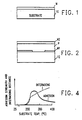
- FIGS. 1 and 2 illustrate representative environments in which the invention can be practiced to provide improved structures.
- a substrate 10 has a metal layer M thereon.
- Substrate 10 is one of the organic substrates described hereinabove, while metal layer M is one of the aforementioned metals which weakly interact with polymer substrate 10.
- FIG. 2 shows a structure of the type which might be present in a semiconductor circuit or package.
- layer 12 can be a semiconductor, a glass, or a ceramic layer which has a first metallic coating M1 thereon, and a layer of electrically insulating material such as a polymer P.
- a polymer which is often used for this purpose is polyimide.
- a second metal layer M2 which is a metal that weakly bonds with the polymer layer P.
- the first example is the deposition of copper layers onto polyimide substrates.
- the copper layers were evaporated from small beads, molten onto a tungsten wire in vacuum.
- the evaporation rate was of the order of 2 angstroms per minute.
- the polyimide substrates were prepared by spinning a thin layer of polyimide onto an A1-coated Si substrate and then curing the sample (annealing in an inert gas ambient) to cause imidization. After mounting in an ultra high vacuum (UHV) chamber, the samples were annealed at 300°C for five minutes to desorb the water present in the polyimide film. Copper was evaporated on these films at room temperature (25°C), and at elevated temperatures. As will be seen, temperatures of 150°C, 250°C, and 300°C were chosen. Ion scattering analysis to determine the presence of copper in polyimide was performed at room temperature.
- MEIS medium energy ion scattering
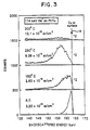
- FIG. 3 shows an energy spectrum for different samples of copper evaporated on polyimide. Samples were evaporated at room temperature (R.T.), 150°C, 250°C, and 300°C. The number of counts of backscattered ions is plotted against the backscattered energy for each of these four samples. The number of copper atomstcm 2 evaporated on the samples is indicated for each substrate deposition temperature. Copper at the surface is indicated by the vertical line 14 at the right hand side of this energy distribution plot, while the numeral "2" is merely a scale factor.
- the copper forms clusters (spheres) at all of the temperatures which were studied. After deposition at 300°K, the copper spheres do not grow upon annealing. The copper atoms have become immobile and are only covered by a thin polyimide film upon annealing. However, with increasing deposition temperature the size of the copper spheres increases. At a given temperature, the spheres all have approximately the same size.
- the copper atoms arrive at the polyimide surface one by one. They do not interact with other copper atoms arriving on the surface at the same time.
- the individual copper atoms do not have a strong chemical interaction with the polyimide. However, they can diffuse freely through the polyimide.
- the diffusion length of the copper in the polyimide is limited by the temperature. Thus, at room temperature the copper atoms do not diffuse very deeply into the polyimide, but at high temperatures they do.
- the copper atoms diffuse around until they meet other copper atoms with which they conform a cluster. Such clustering is favourable because of the cohesive energy of solid copper.
- Copper is characteristic of metals which intrinsically weakly bond with these organic substrates.
- This critical temperature range occurs at temperatures less than the curing or glass transition temperatures of the substrate.
- These metal-polymer interfaces follow a physical characteristic, in contrast with those wherein stronger chemical processes occur. In the latter situation, these strong chemical processes are likely to arrest strong diffusion and give rise to much sharper interfaces which are less affected by the deposition temperature. In fact, this has been seen for the deposition of Cr on polyimide, wherein a critical temperature range for maximum adhesion, less than the substrate curing temperature, was not found.
- FIG. 4 plots adhesion strength and intermixing distance versus substrate temperature, and illustrates what is meant by optimum intermixing.
- Intermixing is generally increased as substrate temperature increases, due to enhanced diffusion of metal atoms into the substrate.
- the distance into the substrate through which the metal atoms diffuse also increases. This is indicated by the dashed curve in FIG. 4, showing a generally increasing distance over which intermixing occurs.
- FIGS. 5 and 6 plot the peel strength, measured in grams per millimeter, against substrate evaporation temperature for copper samples of various widths deposited on polyimide.
- FIG. 5 covers the temperature range of room temperature (RT)-280°C for some samples, while FIG. 6 covers the temperature range 240°C-360°C for other samples. The samples were measured before and after baking at 300°C in a nitrogen atmosphere. From the curves of FIG. 5, it is apparent that a maximum adhesion strength for these samples exists at a temperature range 240-280°C, and more particularly at approximately 260°C. This critical substrate range existed for all of the samples of copper on polyimide, regardless of the sample width.
- FIG. 6 plots the peel strength of other copper samples on polyimide versus the substrate evaporation temperature, for four temperatures: 240, 280, 320, and 360°C. Plots are shown for samples which have been nitrogen baked and for these samples before nitrogen baking. For these samples, the peel strength was maximized at a deposition temperature of 240°C, and diminished thereafter. The difference between these samples and those depicted in FIG. 5 relates to the different treatment given to each set of samples.
- the second set of samples (FIG. 6) didn't go through the whole temperature range from approximately 100°C, so the overall behaviour for these samples is not as clear. However, the results do indicate the degradation of adhesion due to excess diffusion at high temperatures. This means that an optimum intermixing is important.
- nickel was deposited on polyimide at different temperatures ranging from room temperature to 360°C.
- maximum intermixing, and therefore adhesion occurs at a critical temperature range less than the c-cure temperature (360°C) commonly used to cure the polyimide substrate.
- the temperature range 240-280°C is also very favourable for nickel deposition.
- copper and nickel were deposited on polyimide, and the peel adhesion strength of the samples in grams/mm, was measured. This was done for samples deposited at different deposition temperatures, with and without post-annealing.
- the nickel samples were approximately 1000 angstroms thick, while the copper samples were 8 microns thick.
- the deposition rate for the copper and nickel samples was about 10 angstroms/second.
- Substrate heating is used shortly before (one hour or less) metal deposition, and during metal deposition.
- metal deposition is used shortly before (one hour or less) metal deposition, and during metal deposition.
- intermixing is complete and the substrate temperature as well as the deposition rate can be changed to continue growing the rest of the film.
- Table II shows data corresponding to other Ni-polyimide interfaces where the adhesion strength has been measured as a function of deposition temperature and diffusion annealing.
- the present data indicates that maximum peel adhesion strength was found for depositions at 280°C, for all samples, i.e., without regard to the annealing process.
- This high peel adhesion strength for samples deposited at 280°C was found to be maintained even under a very detrimental temperature and humidity (T and H) test which subjected the samples to 1000 hours at 85°C and 80% relative humidity.
- T and H temperature and humidity
- the actual technique for depositing metal atoms is not critical. Any suitable technique, such as evaporation or sputtering, can be used. Also, the results showing improved adhesion at critical substrate temperature less than the curing temperature remain, regardless of post deposition conditions (such as post-annealing). The important factor is the optimization of intermixing during the initial stages of metal deposition.
- Combinations of metals can be deposited at the same time onto the substrate, and the substrate temperature can be adjusted within the critical temperature range for different deposition rates, in order to tailor the amount of adhesion between the metal and the substrate.
- T c The temperature range of approximately (0.6-0.8) T c is substantially definite, but does include some leeway in it, such as a few degrees outside 0.6 T c and 0.8 T c .
- a usable upper temperature can approach 0.85 T..
Landscapes
- Chemical & Material Sciences (AREA)
- Engineering & Computer Science (AREA)
- Materials Engineering (AREA)
- Manufacturing & Machinery (AREA)
- Microelectronics & Electronic Packaging (AREA)
- Chemical Kinetics & Catalysis (AREA)
- Inorganic Chemistry (AREA)
- Mechanical Engineering (AREA)
- Metallurgy (AREA)
- Organic Chemistry (AREA)
- Physical Vapour Deposition (AREA)
- Manufacturing Of Printed Wiring (AREA)
- Laminated Bodies (AREA)
Claims (7)
Applications Claiming Priority (2)
| Application Number | Priority Date | Filing Date | Title |
|---|---|---|---|
| US69056785A | 1985-01-11 | 1985-01-11 | |
| US690567 | 1985-01-11 |
Publications (3)
| Publication Number | Publication Date |
|---|---|
| EP0187706A2 EP0187706A2 (de) | 1986-07-16 |
| EP0187706A3 EP0187706A3 (en) | 1987-09-02 |
| EP0187706B1 true EP0187706B1 (de) | 1989-12-13 |
Family
ID=24772994
Family Applications (1)
| Application Number | Title | Priority Date | Filing Date |
|---|---|---|---|
| EP86300070A Expired EP0187706B1 (de) | 1985-01-11 | 1986-01-07 | Verfahren zur Metallbeschichtung eines organischen Substrates |
Country Status (4)
| Country | Link |
|---|---|
| EP (1) | EP0187706B1 (de) |
| JP (1) | JP2605010B2 (de) |
| CA (1) | CA1276088C (de) |
| DE (1) | DE3667498D1 (de) |
Cited By (7)
| Publication number | Priority date | Publication date | Assignee | Title |
|---|---|---|---|---|
| GB2231588A (en) * | 1989-05-02 | 1990-11-21 | Minnesota Mining & Mfg | Noble metal-polymer composites for use in microelectrode stimulation arrays |
| US4975327A (en) * | 1989-07-11 | 1990-12-04 | Minnesota Mining And Manufacturing Company | Polyimide substrate having a textured surface and metallizing such a substrate |
| EP0390188A3 (en) * | 1989-03-31 | 1990-12-27 | Tecnopart S.R.L. | Formed articles based on polymeric material and showing improved wettability and adhesion and process for the production thereof |
| EP0337445A3 (de) * | 1988-04-13 | 1991-01-16 | Hitachi, Ltd. | Laminare Struktur bestehend aus einem organischen Material und aus einem anorganischen Material, Methoden zu ihrer Herstellung und ihrer Benutzung |
| EP0344504A3 (de) * | 1988-06-03 | 1991-05-02 | International Business Machines Corporation | Artikel mit einem Polyimid und einer Metallschicht und Verfahren zum Herstellen solcher Artikel |
| US5178957A (en) * | 1989-05-02 | 1993-01-12 | Minnesota Mining And Manufacturing Company | Noble metal-polymer composites and flexible thin-film conductors prepared therefrom |
| US5183692A (en) * | 1991-07-01 | 1993-02-02 | Motorola, Inc. | Polyimide coating having electroless metal plate |
Families Citing this family (9)
| Publication number | Priority date | Publication date | Assignee | Title |
|---|---|---|---|---|
| DE4211956C1 (de) * | 1992-04-09 | 1993-05-06 | Multi-Arc Oberflaechentechnik Gmbh, 5060 Bergisch Gladbach, De | |
| JPH08330728A (ja) * | 1995-05-26 | 1996-12-13 | Toyo Metaraijingu Kk | フレキシブルプリント配線用基板 |
| US6303278B1 (en) | 1997-01-31 | 2001-10-16 | Cuptronic Ab | Method of applying metal layers in distinct patterns |
| SE508280C2 (sv) * | 1997-01-31 | 1998-09-21 | Cuptronic Ab | Förfarande för att öka vidhäftningsförmågan hos ledande material till ytskikt av polymermaterial |
| DE10026540A1 (de) * | 2000-05-27 | 2001-11-29 | Gfe Met & Mat Gmbh | Gegenstand, insbesondere Implantat |
| JP4605454B2 (ja) * | 2005-03-23 | 2011-01-05 | 住友金属鉱山株式会社 | フレキシブル基板の製造方法 |
| DE602007001344D1 (de) * | 2006-04-10 | 2009-07-30 | Linea Tergi Ltd | Verfahren zur applizierung eines metalls auf ein substrat |
| DK2004907T3 (da) * | 2006-04-10 | 2009-10-19 | Linea Tergi Ltd | Fremgangsmåde til påföring af et metal på papir |
| JP2016159606A (ja) * | 2015-03-05 | 2016-09-05 | 住友電気工業株式会社 | 積層構造体 |
Family Cites Families (11)
| Publication number | Priority date | Publication date | Assignee | Title |
|---|---|---|---|---|
| US2812270A (en) * | 1954-01-28 | 1957-11-05 | Continental Can Co | Method and apparatus for depositing metal coatings on metal bases |
| US2859130A (en) * | 1954-06-16 | 1958-11-04 | Ohio Commw Eng Co | Method for gas plating synthetic fibers |
| US2897091A (en) * | 1954-10-27 | 1959-07-28 | Ohio Commw Eng Co | Method of high speed gas plating of synthetic resins |
| GB1370893A (en) * | 1971-02-09 | 1974-10-16 | Ici Ltd | Metallised thermoplastic films |
| DE2234510A1 (de) * | 1972-07-13 | 1974-01-24 | Siemens Ag | Verfahren zum metallisieren einer zur herstellung von elektrischen kondensatoren dienenden isolierstoffolie |
| JPS538376A (en) * | 1976-07-12 | 1978-01-25 | Ulvac Corp | Preparation of magnetic recording material by evaporation process with oblique incidence |
| FR2378815A1 (fr) * | 1977-01-28 | 1978-08-25 | Paris Haute Lunette | Procede d'application d'un produit de traitement sur des objets en verre organique, tels que des verres de lunette |
| JPS53135840A (en) * | 1977-04-30 | 1978-11-27 | Sumitomo Electric Ind Ltd | Metal coating method for non-electroconductive material |
| DE3136283C1 (de) * | 1981-09-12 | 1983-02-03 | Nukem Gmbh, 6450 Hanau | Verfahren zum Metallisieren kohlefaserverstaerkter Kunststoffteile |
| DE3233087A1 (de) * | 1982-09-07 | 1984-03-08 | Ibm Deutschland Gmbh, 7000 Stuttgart | Verfahren zum herstellen von duennen metallschichten mittels aufdampfens |
| US4466875A (en) * | 1983-11-30 | 1984-08-21 | Ppg Industries, Inc. | Auxiliary heater for magnetron sputtering |
-
1985
- 1985-09-12 JP JP60200729A patent/JP2605010B2/ja not_active Expired - Lifetime
- 1985-12-20 CA CA000498399A patent/CA1276088C/en not_active Expired
-
1986
- 1986-01-07 EP EP86300070A patent/EP0187706B1/de not_active Expired
- 1986-01-07 DE DE8686300070T patent/DE3667498D1/de not_active Expired - Lifetime
Cited By (9)
| Publication number | Priority date | Publication date | Assignee | Title |
|---|---|---|---|---|
| EP0337445A3 (de) * | 1988-04-13 | 1991-01-16 | Hitachi, Ltd. | Laminare Struktur bestehend aus einem organischen Material und aus einem anorganischen Material, Methoden zu ihrer Herstellung und ihrer Benutzung |
| US5084355A (en) * | 1988-04-13 | 1992-01-28 | Hitachi, Ltd. | Laminar structure comprising organic material and inorganic material |
| EP0344504A3 (de) * | 1988-06-03 | 1991-05-02 | International Business Machines Corporation | Artikel mit einem Polyimid und einer Metallschicht und Verfahren zum Herstellen solcher Artikel |
| EP0390188A3 (en) * | 1989-03-31 | 1990-12-27 | Tecnopart S.R.L. | Formed articles based on polymeric material and showing improved wettability and adhesion and process for the production thereof |
| GB2231588A (en) * | 1989-05-02 | 1990-11-21 | Minnesota Mining & Mfg | Noble metal-polymer composites for use in microelectrode stimulation arrays |
| US5178957A (en) * | 1989-05-02 | 1993-01-12 | Minnesota Mining And Manufacturing Company | Noble metal-polymer composites and flexible thin-film conductors prepared therefrom |
| US4975327A (en) * | 1989-07-11 | 1990-12-04 | Minnesota Mining And Manufacturing Company | Polyimide substrate having a textured surface and metallizing such a substrate |
| EP0408205A1 (de) * | 1989-07-11 | 1991-01-16 | Minnesota Mining And Manufacturing Company | Polyimidsubstrat mit texturierter Oberfläche und Metallbeschichtung solch eines Substrates |
| US5183692A (en) * | 1991-07-01 | 1993-02-02 | Motorola, Inc. | Polyimide coating having electroless metal plate |
Also Published As
| Publication number | Publication date |
|---|---|
| CA1276088C (en) | 1990-11-13 |
| JPS61164295A (ja) | 1986-07-24 |
| DE3667498D1 (de) | 1990-01-18 |
| JP2605010B2 (ja) | 1997-04-30 |
| EP0187706A2 (de) | 1986-07-16 |
| EP0187706A3 (en) | 1987-09-02 |
Similar Documents
| Publication | Publication Date | Title |
|---|---|---|
| US4720401A (en) | Enhanced adhesion between metals and polymers | |
| EP0187706B1 (de) | Verfahren zur Metallbeschichtung eines organischen Substrates | |
| US5622608A (en) | Process of making oxidation resistant high conductivity copper layers | |
| US5580668A (en) | Aluminum-palladium alloy for initiation of electroless plating | |
| US20100190029A1 (en) | Metal layer laminate having roughened metal surface layer and method for producing the same | |
| US11798815B2 (en) | Method of metalizing a glass article | |
| US7154045B2 (en) | Wired circuit board | |
| US5631498A (en) | Thin film metallization process for improved metal to substrate adhesion | |
| JPS62171187A (ja) | 印刷回路板の製造方法 | |
| EP0351533B1 (de) | Verfahren zur Beschichtung eines Substrats mit einer Metallschicht | |
| Callegari et al. | Adhesion durability of tantalum BPDA‐PDA polyimide interfaces | |
| CN111132466A (zh) | 一种阻止pcb表面发生金属离子迁移的方法 | |
| JP2501791B2 (ja) | フイルムキヤリヤ形基板とその製造方法 | |
| EP0564693A1 (de) | Substrat von Filmträgertyp und Herstellungsverfahren dafür | |
| JP2960644B2 (ja) | 表面処理された窒化アルミニウム基材 | |
| CN217933782U (zh) | 一种附着于半导体硅芯片表面的金属接触层 | |
| TWI921630B (zh) | 一種覆銅層壓膜及包括其的電子器件 | |
| JPH04346651A (ja) | メタライジング法 | |
| JP2986948B2 (ja) | AlN回路基板 | |
| JP3079765B2 (ja) | 電気接点用材料 | |
| JPS6214445A (ja) | エレクトロニクス部品用複合材料 | |
| JP3060709B2 (ja) | 電気接点用材料の製造方法および製造装置 | |
| JPS62122152A (ja) | 半導体装置用基板の製造方法 | |
| KR20240124753A (ko) | 하이브리드 구리 금속화 | |
| JPH05151827A (ja) | 導体付き基板 |
Legal Events
| Date | Code | Title | Description |
|---|---|---|---|
| PUAI | Public reference made under article 153(3) epc to a published international application that has entered the european phase |
Free format text: ORIGINAL CODE: 0009012 |
|
| AK | Designated contracting states |
Kind code of ref document: A2 Designated state(s): DE FR GB IT |
|
| 17P | Request for examination filed |
Effective date: 19861125 |
|
| PUAL | Search report despatched |
Free format text: ORIGINAL CODE: 0009013 |
|
| AK | Designated contracting states |
Kind code of ref document: A3 Designated state(s): DE FR GB IT |
|
| 17Q | First examination report despatched |
Effective date: 19890322 |
|
| GRAA | (expected) grant |
Free format text: ORIGINAL CODE: 0009210 |
|
| AK | Designated contracting states |
Kind code of ref document: B1 Designated state(s): DE FR GB IT |
|
| REF | Corresponds to: |
Ref document number: 3667498 Country of ref document: DE Date of ref document: 19900118 |
|
| ET | Fr: translation filed | ||
| ITF | It: translation for a ep patent filed | ||
| PLBE | No opposition filed within time limit |
Free format text: ORIGINAL CODE: 0009261 |
|
| STAA | Information on the status of an ep patent application or granted ep patent |
Free format text: STATUS: NO OPPOSITION FILED WITHIN TIME LIMIT |
|
| 26N | No opposition filed | ||
| ITTA | It: last paid annual fee | ||
| PGFP | Annual fee paid to national office [announced via postgrant information from national office to epo] |
Ref country code: GB Payment date: 19951215 Year of fee payment: 11 |
|
| PGFP | Annual fee paid to national office [announced via postgrant information from national office to epo] |
Ref country code: FR Payment date: 19960103 Year of fee payment: 11 |
|
| PGFP | Annual fee paid to national office [announced via postgrant information from national office to epo] |
Ref country code: DE Payment date: 19960126 Year of fee payment: 11 |
|
| PG25 | Lapsed in a contracting state [announced via postgrant information from national office to epo] |
Ref country code: GB Effective date: 19970107 |
|
| GBPC | Gb: european patent ceased through non-payment of renewal fee |
Effective date: 19970107 |
|
| PG25 | Lapsed in a contracting state [announced via postgrant information from national office to epo] |
Ref country code: FR Effective date: 19970930 |
|
| PG25 | Lapsed in a contracting state [announced via postgrant information from national office to epo] |
Ref country code: DE Effective date: 19971001 |
|
| REG | Reference to a national code |
Ref country code: FR Ref legal event code: ST |
|
| PG25 | Lapsed in a contracting state [announced via postgrant information from national office to epo] |
Ref country code: IT Free format text: LAPSE BECAUSE OF NON-PAYMENT OF DUE FEES;WARNING: LAPSES OF ITALIAN PATENTS WITH EFFECTIVE DATE BEFORE 2007 MAY HAVE OCCURRED AT ANY TIME BEFORE 2007. THE CORRECT EFFECTIVE DATE MAY BE DIFFERENT FROM THE ONE RECORDED. Effective date: 20050107 |