EP0187718A2 - Halbleiterlaser mit verteilter Rückkopplung - Google Patents
Halbleiterlaser mit verteilter Rückkopplung Download PDFInfo
- Publication number
- EP0187718A2 EP0187718A2 EP86300127A EP86300127A EP0187718A2 EP 0187718 A2 EP0187718 A2 EP 0187718A2 EP 86300127 A EP86300127 A EP 86300127A EP 86300127 A EP86300127 A EP 86300127A EP 0187718 A2 EP0187718 A2 EP 0187718A2
- Authority
- EP
- European Patent Office
- Prior art keywords
- layer
- semiconductor laser
- absorption layer
- laser device
- distributed feedback
- Prior art date
- Legal status (The legal status is an assumption and is not a legal conclusion. Google has not performed a legal analysis and makes no representation as to the accuracy of the status listed.)
- Granted
Links
Images
Classifications
-
- H—ELECTRICITY
- H01—ELECTRIC ELEMENTS
- H01S—DEVICES USING THE PROCESS OF LIGHT AMPLIFICATION BY STIMULATED EMISSION OF RADIATION [LASER] TO AMPLIFY OR GENERATE LIGHT; DEVICES USING STIMULATED EMISSION OF ELECTROMAGNETIC RADIATION IN WAVE RANGES OTHER THAN OPTICAL
- H01S5/00—Semiconductor lasers
- H01S5/10—Construction or shape of the optical resonator, e.g. extended or external cavity, coupled cavities, bent-guide, varying width, thickness or composition of the active region
- H01S5/12—Construction or shape of the optical resonator, e.g. extended or external cavity, coupled cavities, bent-guide, varying width, thickness or composition of the active region the resonator having a periodic structure, e.g. in distributed feedback [DFB] lasers
- H01S5/1228—DFB lasers with a complex coupled grating, e.g. gain or loss coupling
-
- H—ELECTRICITY
- H01—ELECTRIC ELEMENTS
- H01S—DEVICES USING THE PROCESS OF LIGHT AMPLIFICATION BY STIMULATED EMISSION OF RADIATION [LASER] TO AMPLIFY OR GENERATE LIGHT; DEVICES USING STIMULATED EMISSION OF ELECTROMAGNETIC RADIATION IN WAVE RANGES OTHER THAN OPTICAL
- H01S5/00—Semiconductor lasers
- H01S5/20—Structure or shape of the semiconductor body to guide the optical wave ; Confining structures perpendicular to the optical axis, e.g. index or gain guiding, stripe geometry, broad area lasers, gain tailoring, transverse or lateral reflectors, special cladding structures, MQW barrier reflection layers
- H01S5/22—Structure or shape of the semiconductor body to guide the optical wave ; Confining structures perpendicular to the optical axis, e.g. index or gain guiding, stripe geometry, broad area lasers, gain tailoring, transverse or lateral reflectors, special cladding structures, MQW barrier reflection layers having a ridge or stripe structure
- H01S5/223—Buried stripe structure
- H01S5/2232—Buried stripe structure with inner confining structure between the active layer and the lower electrode
Definitions
- This invention relates to a distributed feedback semiconductor laser device, the absorption loss of which has been changed at the same periodicity as the wavelength of laser light in the direction of ' the propagation of the laser light, thereby allowing oscillation in a single longitudinal mode.
- the facets of both ends of the devices do not result in those of a Fabry-Perot resonator, but rather, one of the facets is etched diagonally, so that the asymmetry of the resonator is increased greatly, and stable single-mode oscillation can be achieved.
- the semiconductor laser device with a distributed feedback of this invention which overcomes the above-discussed and numerous other disadvantages and deficiencies of the prior art, comprises an active layer positioned between a first cladding layer and a second cladding layer, and an absorption layer positioned between said active layer and one of said cladding layers, said absorption layer having grooves to form a diffraction grating with a given periodicity in the direction of the propagation of laser light.
- a buffer layer having the same polarity as said cladding layer is, in a preferred embodiment, positioned between said active layer and said absorption layer.
- the absorption layer has an energy gap which is equal to or is somewhat narrower than that of said active layer and has the same polarity as said cladding layer.
- the absorption layer has a different polarity from that of said cladding layer and a reverse bias is applied to the junction at the interface between said buffer layer and said absorption layer, resulting in a current blocking structure having a diffraction grating with the same periodicity as the diffraction grating of said absorption layer.
- the invention described herein makes possible the objects (1) of providing a distributed feedback semiconductor laser device in which an absorption layer is disposed between the active layer and one of the two cladding layers to achieve a change of the absorption coefficient of laser light at the same periodicity as the wavelength of the laser light in the direction of the propagation of the laser light thereby allowing for the existence of only one longitudinal mode with maximum gain, so that the laser device can oscillate in a single longitudinal mode in operation not only under a steady state but also under an unsteady state, and neither broadening of the oscillation spectrum nor noncontinuous change in the oscillation mode arise; (2) a distributed feedback semiconductor laser device in which, since a buffer layer with a limited thickness is disposed between the active layer and the absorption layer, laser light is sensitive enough to the periodic structure of the absorption layer to be oscillated in a single longitudinal mode; (3) a distributed feedback semiconductor laser device in which reverse bias voltage is applied to the heterojunction at the interface between the buffer layer and the absorption layer to achieve a change of the absorption coefficient of the laser light
- the semiconductor laser device of this invention is a distributed feedback semiconductor laser device of a double heterostructure type designed in such a manner that an absorption layer, having a limited thickness with a regular periodicity along the direction of the propagation of laser light, is disposed between the active layer and one of the cladding layers, thereby achieving a change of gain or the absorption coefficient to match the periodicity of the wavelength of the laser light.
- this distributed feedback semiconductor laser device there is only one longitudinal mode with maximum gain, and oscillation is attained in a single longitudinal mode even in operation under an unsteady state where the excitation current is rapidly modulated as when it is being used as a light source for optical communication.
- Distributed feedback semiconductor laser devices in which the gain or the absorption coefficient changes periodically have not yet proposed.
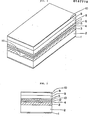
- a p-Ga 0.75 Al 0.25 As cladding layer (the first cladding layer) 4 a Ga 0.99 Al 0.01 As active layer 5, an n-Ga 0.75 Al 0.25 As buffer layer 6 and an n-GaAs absorption layer 7 are successively grown by liquid phase epitaxy.
- the energy gap Eg of the GaAs absorption layer 7 is smaller than that of any Ga x Al 1-x As layer (namely, the energy gap Eg of the GaAs absorption layer 7 is smaller than that of the Ga 0,99 Al 0.01 As active layer 5), and accordingly the resulting laser light resonator has an effective absorption coefficient.
- the buffer layer 6 is not necessarily required, but when it is formed with a limited thickness, a desired oscillation in a single longitudinal mode can be attained even in operation under an unsteady state as described in detail below.
- a photo-resist is coated on the n-GaAs absorption layer 7 to form a photo-resist mask in the form of a diffraction grating with the same periodicity as the wavelength of laser light by means of a holographic exposing system (not shown).
- the buffer layer 6 is composed of a GaAlAs layer and once it is exposed to air it is oxidized to thereby make it difficult to be subjected to the subsequent liquid phase epitaxial treatment.
- an n-Ga 0.75 Al 0.25 As cladding layer (the second cladding layer) 8 and an n-GaAs cap layer 9 are successively grown by liquid phase epitaxy. Electrodes 1 and 10 are formed on the back face of the substrate 2 and on the upper face of the cap layer 9, respectively, by vacuum evaporation.
- the influence of the laser light on the periodic structure of the above-mentioned absorption layer 7 depends upon both the amplitude at the point of the periodical change of the thickness of the absorption layer 7 and the thickness of the buffer layer 6.
- the thickness of the buffer layer 6 is extremely thin, the laser light becomes sensitive to the periodic structure of the absorption layer 7, but the laser light is absorbed to a large extent in the optical waveguide so that the threshold current level for oscillation will become high.
- Such an undesirable phenomenon can be prevented if the thickness of the absorption layer 7 is sufficiently thin.
- the amplitude must be 800 A at maximum.
- the formation of the buffer layer 6 with a limited thickness makes it possible to make the laser light sensitive to the periodic structure of the absorption layer 7, so that oscillation in a single longitudinal mode can be attained even in operation under an unsteady state. This is because the absorption coefficient.of the device changes to the same center-to-center spacing as the wavelength of the laser light in the direction of the propagation of the laser light and thus there is only one longitudinal mode with maximum gain.
- Figure 2 shows another semiconductor laser device of this invention, which is the same structure as disclosed in Figure 1 except that the p-GaAlAs buffer layer 13 and the p-GaAs absorption layer 12 are positioned under the active layer 5.
- the polarity of the GaAs absorption layer 12 must be the same p-type as that of the p-Ga 0.75 Al 0.25 As cladding layer (the first cladding layer) 4.
- each of the above-mentioned Figures 1 and 2 discloses only an inner striped GaAlAs/GaAs double-heterostructure semiconductor laser device, it is not limited thereto.
- Semiconductor laser devices using other materials such as InGaAsP/InP, etc., can be applied.
- semiconductor laser devices having the same sectional view as a buried type laser device can be applied.
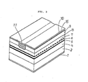
- Figure 3 shows another distributed feedback semiconductor laser device of this invention, which comprises a first n-InP cladding layer 4, an In x Ga 1-x As y P 1-y (0.47 ⁇ x ⁇ 1 and 0 ⁇ y ⁇ 1) active layer 5, a p-InP buffer layer 6, an n-InP absorption layer 7 formed in a diffraction grating and a second p-InP cladding layer 8, in sequence.
- a reverse bias is applied to the junction at the interface between the p-InP buffer layer 6 and the n-InP absorption layer 7.
- All of the p-InP buffer layer 6, the n-InP absorption layer 7 and the p-InP cladding layer 8 are not necessarily of the same materials, but the p-InP buffer layer 6 must be the same polarity as the p-InP cladding layer 8 and the energy gap of each of the buffer layer 6 and the cladding layer 8 must be greater than that of the active layer 5.
- the polarity of the absorption layer 7 must be different from that of each of the InP buffer layer 6 and the InP cladding layer 8.
- This semiconductor laser device is produced as follows: On an n-InP substrate 2, the first n-InP cladding layer 4, the active layer 5 having the composition ratio required to create an oscillation wavelength ranging from approximately 1.1 ⁇ m to approximately 1.6 ⁇ m, the p-InP buffer layer 6 having a thickness of approximately 0.08 ⁇ m and the n-InP absorption layer 7 having a thickness of approximately 0.1 ⁇ m are successively grown by liquid phase epitaxy.
- a photo-resist is coated on the n-InP absorption layer 7 to form a photo-resist mask (not shown) in the form of a diffraction grating with the same periodicity as the wavelength of laser light by the exposure of an interference fringe pattern with a center-to-center spacing 0 0 in a range of 1700 A to 2500 A by means of a holographic exposing system or the like.
- the second p-InP cladding layer 8 and an n-InP cap layer 9 are successively grown, followed by a plasma chemical vapor deposition treatment to form a SiNx film 15 having a thickness of 0 approximately 2000 A.
- An impurity element such as Z n is then diffused into the cap layer 9 and the cladding layer 8 to form a p-channel 11 functioning as an electric current path while the SiNx film 15 is used as a diffusion mask.
- electrodes 1 and 10 are formed on the upper face of the SiNx film 15 including the channel 11 and the back face of the substrate 2, respectively, resulting in a distributed feedback semiconductor laser device.
- the semiconductor laser device of this invention achieves oscillation in a stabilized single longitudinal mode in operation not only under a steady state but also under an unsteady state.
Landscapes
- Physics & Mathematics (AREA)
- Condensed Matter Physics & Semiconductors (AREA)
- General Physics & Mathematics (AREA)
- Electromagnetism (AREA)
- Optics & Photonics (AREA)
- Semiconductor Lasers (AREA)
Applications Claiming Priority (4)
| Application Number | Priority Date | Filing Date | Title |
|---|---|---|---|
| JP309985A JPH067624B2 (ja) | 1985-01-10 | 1985-01-10 | 半導体レ−ザ−装置 |
| JP3099/85 | 1985-01-10 | ||
| JP60023169A JPS61182295A (ja) | 1985-02-07 | 1985-02-07 | 半導体レ−ザ装置 |
| JP23169/85 | 1985-02-07 |
Publications (3)
| Publication Number | Publication Date |
|---|---|
| EP0187718A2 true EP0187718A2 (de) | 1986-07-16 |
| EP0187718A3 EP0187718A3 (en) | 1988-06-01 |
| EP0187718B1 EP0187718B1 (de) | 1994-04-06 |
Family
ID=26336608
Family Applications (1)
| Application Number | Title | Priority Date | Filing Date |
|---|---|---|---|
| EP86300127A Expired - Lifetime EP0187718B1 (de) | 1985-01-10 | 1986-01-09 | Halbleiterlaser mit verteilter Rückkopplung |
Country Status (3)
| Country | Link |
|---|---|
| US (1) | US4716570A (de) |
| EP (1) | EP0187718B1 (de) |
| DE (1) | DE3689756T2 (de) |
Cited By (2)
| Publication number | Priority date | Publication date | Assignee | Title |
|---|---|---|---|---|
| EP0356135A3 (en) * | 1988-08-17 | 1990-09-12 | Sharp Kabushiki Kaisha | A semiconductor laser device |
| GB2232814A (en) * | 1989-05-22 | 1990-12-19 | Mitsubishi Electric Corp | A semiconductor laser device |
Families Citing this family (7)
| Publication number | Priority date | Publication date | Assignee | Title |
|---|---|---|---|---|
| JPS62144378A (ja) * | 1985-12-18 | 1987-06-27 | Sony Corp | 分布帰還覆半導体レ−ザ− |
| JPH073909B2 (ja) * | 1987-09-08 | 1995-01-18 | 三菱電機株式会社 | 半導体レーザの製造方法 |
| US4904045A (en) * | 1988-03-25 | 1990-02-27 | American Telephone And Telegraph Company | Grating coupler with monolithically integrated quantum well index modulator |
| KR940007605B1 (ko) * | 1991-11-07 | 1994-08-20 | 주식회사 금성사 | 반도체 레이저 다이오드 제조방법 |
| JP2705409B2 (ja) * | 1991-11-21 | 1998-01-28 | 三菱電機株式会社 | 半導体分布帰還形レーザ装置 |
| JP3714984B2 (ja) * | 1995-03-06 | 2005-11-09 | シャープ株式会社 | 分布帰還型半導体レーザ装置 |
| JP2001266389A (ja) * | 2000-03-23 | 2001-09-28 | Tdk Corp | 近接場光を用いる光ヘッド |
Family Cites Families (11)
| Publication number | Priority date | Publication date | Assignee | Title |
|---|---|---|---|---|
| US4178604A (en) * | 1973-10-05 | 1979-12-11 | Hitachi, Ltd. | Semiconductor laser device |
| JPS51146196A (en) * | 1975-06-11 | 1976-12-15 | Hitachi Ltd | Diode laser |
| US4045749A (en) * | 1975-11-24 | 1977-08-30 | Xerox Corporation | Corrugation coupled twin guide laser |
| US4233090A (en) * | 1979-06-28 | 1980-11-11 | Rca Corporation | Method of making a laser diode |
| JPS57170584A (en) * | 1981-04-15 | 1982-10-20 | Hitachi Ltd | Semiconductor laser device |
| JPS5861693A (ja) * | 1981-10-09 | 1983-04-12 | Kokusai Denshin Denwa Co Ltd <Kdd> | 分布帰還形半導体レ−ザ |
| JPS58140177A (ja) * | 1982-02-16 | 1983-08-19 | Kokusai Denshin Denwa Co Ltd <Kdd> | 分布帰還形半導体レ−ザ |
| EP0106305B1 (de) * | 1982-10-12 | 1989-03-15 | Nec Corporation | Doppelheterostruktur-Halbleiterlaser mit periodischer Struktur der Wellenleiterschicht |
| JPS59125685A (ja) * | 1983-01-06 | 1984-07-20 | Nec Corp | 分布帰還型埋め込み構造半導体レ−ザ |
| JPS59127892A (ja) * | 1983-01-11 | 1984-07-23 | Nec Corp | 半導体レ−ザとその製造方法 |
| JPS59151483A (ja) * | 1983-02-18 | 1984-08-29 | Agency Of Ind Science & Technol | 半導体レ−ザ装置 |
-
1986
- 1986-01-06 US US06/816,259 patent/US4716570A/en not_active Expired - Lifetime
- 1986-01-09 EP EP86300127A patent/EP0187718B1/de not_active Expired - Lifetime
- 1986-01-09 DE DE3689756T patent/DE3689756T2/de not_active Expired - Lifetime
Cited By (5)
| Publication number | Priority date | Publication date | Assignee | Title |
|---|---|---|---|---|
| EP0356135A3 (en) * | 1988-08-17 | 1990-09-12 | Sharp Kabushiki Kaisha | A semiconductor laser device |
| US5027368A (en) * | 1988-08-17 | 1991-06-25 | Sharp Kabushiki Kaisha | Semiconductor laser device |
| GB2232814A (en) * | 1989-05-22 | 1990-12-19 | Mitsubishi Electric Corp | A semiconductor laser device |
| US5020072A (en) * | 1989-05-22 | 1991-05-28 | Mitsubishi Denki Kabushiki Kaisha | Semiconductor laser device |
| GB2232814B (en) * | 1989-05-22 | 1993-04-14 | Mitsubishi Electric Corp | A semiconductor laser device |
Also Published As
| Publication number | Publication date |
|---|---|
| US4716570A (en) | 1987-12-29 |
| EP0187718B1 (de) | 1994-04-06 |
| DE3689756D1 (de) | 1994-05-11 |
| EP0187718A3 (en) | 1988-06-01 |
| DE3689756T2 (de) | 1994-07-21 |
Similar Documents
| Publication | Publication Date | Title |
|---|---|---|
| US4594718A (en) | Combination index/gain guided semiconductor lasers | |
| EP0065818A1 (de) | Phasengekoppelte Halbleiterlaservorrichtung | |
| US4426702A (en) | Semiconductor laser device | |
| EP0064339A1 (de) | Halbleiterlaservorrichtung | |
| US4803691A (en) | Lateral superradiance suppressing diode laser bar | |
| US5126804A (en) | Light interactive heterojunction semiconductor device | |
| US4903274A (en) | Semiconductor laser array device | |
| EP0033137A2 (de) | Halbleiterlaservorrichtung | |
| US4340967A (en) | Semiconductor lasers with stable higher-order modes parallel to the junction plane | |
| US4280108A (en) | Transverse junction array laser | |
| US4575851A (en) | Double channel planar buried heterostructure laser with periodic structure formed in guide layer | |
| US4716570A (en) | Distributed feedback semiconductor laser device | |
| US4868838A (en) | Semiconductor laser device | |
| JPS621296A (ja) | 多端子型半導体レ−ザ素子 | |
| US4718069A (en) | Semiconductor laser array with single lobed output | |
| JPH0461514B2 (de) | ||
| JPS60102789A (ja) | 分布帰環形半導体レ−ザ | |
| US4692925A (en) | Phase-locked laser array | |
| US4837775A (en) | Electro-optic device having a laterally varying region | |
| US4821278A (en) | Inverted channel substrate planar semiconductor laser | |
| US4768200A (en) | Internal current confinement type semiconductor light emission device | |
| US4878223A (en) | Semiconductor laser array device | |
| EP0306314B1 (de) | Halbleiterlaser-Vorrichtung | |
| US4771433A (en) | Semiconductor laser device | |
| US4872174A (en) | Semiconductor laser device having a grating structure |
Legal Events
| Date | Code | Title | Description |
|---|---|---|---|
| PUAI | Public reference made under article 153(3) epc to a published international application that has entered the european phase |
Free format text: ORIGINAL CODE: 0009012 |
|
| 17P | Request for examination filed |
Effective date: 19860127 |
|
| AK | Designated contracting states |
Kind code of ref document: A2 Designated state(s): DE GB NL |
|
| PUAL | Search report despatched |
Free format text: ORIGINAL CODE: 0009013 |
|
| AK | Designated contracting states |
Kind code of ref document: A3 Designated state(s): DE GB NL |
|
| RHK1 | Main classification (correction) |
Ipc: H01S 3/19 |
|
| 17Q | First examination report despatched |
Effective date: 19910715 |
|
| GRAA | (expected) grant |
Free format text: ORIGINAL CODE: 0009210 |
|
| AK | Designated contracting states |
Kind code of ref document: B1 Designated state(s): DE GB NL |
|
| REF | Corresponds to: |
Ref document number: 3689756 Country of ref document: DE Date of ref document: 19940511 |
|
| RIN2 | Information on inventor provided after grant (corrected) |
Free format text: YOSHIDA, TOSHIHIKO * TAKIGUCHI, HARUHISA * KANEIWA, SHINJI 101 KYOBATE MANSION * MATSUI, SADAYOSHI |
|
| K2C1 | Correction of patent specification (title page) published |
Effective date: 19940406 |
|
| PLBE | No opposition filed within time limit |
Free format text: ORIGINAL CODE: 0009261 |
|
| STAA | Information on the status of an ep patent application or granted ep patent |
Free format text: STATUS: NO OPPOSITION FILED WITHIN TIME LIMIT |
|
| 26N | No opposition filed | ||
| REG | Reference to a national code |
Ref country code: GB Ref legal event code: IF02 |
|
| PGFP | Annual fee paid to national office [announced via postgrant information from national office to epo] |
Ref country code: NL Payment date: 20050103 Year of fee payment: 20 |
|
| PGFP | Annual fee paid to national office [announced via postgrant information from national office to epo] |
Ref country code: GB Payment date: 20050105 Year of fee payment: 20 |
|
| PGFP | Annual fee paid to national office [announced via postgrant information from national office to epo] |
Ref country code: DE Payment date: 20050106 Year of fee payment: 20 |
|
| PG25 | Lapsed in a contracting state [announced via postgrant information from national office to epo] |
Ref country code: GB Free format text: LAPSE BECAUSE OF EXPIRATION OF PROTECTION Effective date: 20060108 |
|
| PG25 | Lapsed in a contracting state [announced via postgrant information from national office to epo] |
Ref country code: NL Free format text: LAPSE BECAUSE OF EXPIRATION OF PROTECTION Effective date: 20060109 |
|
| REG | Reference to a national code |
Ref country code: GB Ref legal event code: PE20 |
|
| NLV7 | Nl: ceased due to reaching the maximum lifetime of a patent |
Effective date: 20060109 |