EP0188087B1 - Système d'antennes à microbandes - Google Patents
Système d'antennes à microbandes Download PDFInfo
- Publication number
- EP0188087B1 EP0188087B1 EP85308987A EP85308987A EP0188087B1 EP 0188087 B1 EP0188087 B1 EP 0188087B1 EP 85308987 A EP85308987 A EP 85308987A EP 85308987 A EP85308987 A EP 85308987A EP 0188087 B1 EP0188087 B1 EP 0188087B1
- Authority
- EP
- European Patent Office
- Prior art keywords
- antenna
- layers
- microstrip
- conductive pin
- conductive
- Prior art date
- Legal status (The legal status is an assumption and is not a legal conclusion. Google has not performed a legal analysis and makes no representation as to the accuracy of the status listed.)
- Expired
Links
- 239000011152 fibreglass Substances 0.000 claims description 5
- RYGMFSIKBFXOCR-UHFFFAOYSA-N Copper Chemical compound [Cu] RYGMFSIKBFXOCR-UHFFFAOYSA-N 0.000 claims description 4
- 229910052802 copper Inorganic materials 0.000 claims description 4
- 239000010949 copper Substances 0.000 claims description 4
- 230000005855 radiation Effects 0.000 claims 2
- 239000000758 substrate Substances 0.000 description 7
- 238000000034 method Methods 0.000 description 3
- 238000013459 approach Methods 0.000 description 2
- 230000005540 biological transmission Effects 0.000 description 2
- 230000008878 coupling Effects 0.000 description 2
- 238000010168 coupling process Methods 0.000 description 2
- 238000005859 coupling reaction Methods 0.000 description 2
- 238000001514 detection method Methods 0.000 description 2
- 238000005474 detonation Methods 0.000 description 2
- 230000001939 inductive effect Effects 0.000 description 2
- 229910052751 metal Inorganic materials 0.000 description 2
- 239000002184 metal Substances 0.000 description 2
- 229920006362 Teflon® Polymers 0.000 description 1
- 229910052782 aluminium Inorganic materials 0.000 description 1
- XAGFODPZIPBFFR-UHFFFAOYSA-N aluminium Chemical compound [Al] XAGFODPZIPBFFR-UHFFFAOYSA-N 0.000 description 1
- 239000004020 conductor Substances 0.000 description 1
- 238000000151 deposition Methods 0.000 description 1
- 239000003989 dielectric material Substances 0.000 description 1
- 230000005672 electromagnetic field Effects 0.000 description 1
- 239000012212 insulator Substances 0.000 description 1
- 230000007246 mechanism Effects 0.000 description 1
- 238000009966 trimming Methods 0.000 description 1
Images


Classifications
-
- H—ELECTRICITY
- H01—ELECTRIC ELEMENTS
- H01Q—ANTENNAS, i.e. RADIO AERIALS
- H01Q9/00—Electrically-short antennas having dimensions not more than twice the operating wavelength and consisting of conductive active radiating elements
- H01Q9/04—Resonant antennas
- H01Q9/0407—Substantially flat resonant element parallel to ground plane, e.g. patch antenna
- H01Q9/0414—Substantially flat resonant element parallel to ground plane, e.g. patch antenna in a stacked or folded configuration
-
- H—ELECTRICITY
- H01—ELECTRIC ELEMENTS
- H01Q—ANTENNAS, i.e. RADIO AERIALS
- H01Q21/00—Antenna arrays or systems
- H01Q21/06—Arrays of individually energised antenna units similarly polarised and spaced apart
- H01Q21/061—Two dimensional planar arrays
- H01Q21/065—Patch antenna array
-
- H—ELECTRICITY
- H01—ELECTRIC ELEMENTS
- H01Q—ANTENNAS, i.e. RADIO AERIALS
- H01Q9/00—Electrically-short antennas having dimensions not more than twice the operating wavelength and consisting of conductive active radiating elements
- H01Q9/04—Resonant antennas
- H01Q9/0407—Substantially flat resonant element parallel to ground plane, e.g. patch antenna
- H01Q9/0428—Substantially flat resonant element parallel to ground plane, e.g. patch antenna radiating a circular polarised wave
Definitions
- This invention relates to antennas and more particularly to microstrip antenna systems.
- microstrip antennas referred to in common parlance as "patch antennas" have comprised a planar resonant radiating element parallel to, but separated, from a ground plane by a thin dielectric substrate. They have been fed from the back through the ground plane or from the edge by depositing microstrip lines on the dielectric substrate. Such antennas have been both linearly and circularly polarized.
- microstrip patches have been fed utilizing a microstrip feed that resided on the same substrate that the patch was on. This was convenient in that the feed network could be etched at the same time as the patch circuits. Microstrip tuning elements could also be incorporated into this design to match the voltage standing wave ratio (VSWR) of the patches.
- the problem with this design is its susceptibility to electromagnetic pulses (EMP) from a nuclear detonation.
- EMP electromagnetic pulses
- the ground of the coax or connector terminates on the ground plane of the patch and the center conductor passes up through the ground plane and patch substrate to terminate on the patch itself.
- a problem of this structure is that it also is susceptible to EMP coupling into the system.
- Another problem with the above mentioned patch antennas is that they could not be stacked using either of the known feed mechanisms and achieve a low VSWR through easily implemented impedance matching techniques.
- US-A-4,218,682 to Fosch discloses a multi- band antenna having a plurality of resonant elliptical plate elements overlying each other and separated from each other and from a ground plane by layers of dielectric material.
- a feed line is connected to the smallest of the elliptical plate elements which is also the most remote from the ground plane, the elements being arranged in order of size.
- the elements other than the smallest are connected to the ground plane at their centres.
- EP-A-0,105,103 discloses a microstrip antenna system using microstrip transmission line segments each an odd integral number of quarter wavelengths long as a feed line structure close to a ground plane and coupled to a radiating structure by the electromagnetic field generated by the feed line structure.
- Another object of the invention is to provide a microstrip patch antenna having substantially reduced EMP coupling into the system.
- Still another object of the invention is to provide a stacked microstrip patch antenna which allows the patches to be impedance matched to achieve a low VSWR.
- Yet another object of the invention is to provide a stacked patch antenna having substantially increased bandwidth of the patches.
- a microstrip antenna comprising: a groundplane; one or more pairs of antenna forming dielectric and electrically conducting layers formed on the ground plane beginning with a dielectric layer; a top dielectric layer formed over the one or more pairs of antenna forming layers; a conductive pin passing through the antenna forming layers and electrically isolated from the one or more conductive antenna layers, said conductive pin being connectable to an antenna feed below the ground plane, said antenna being characterized by a microstrip open circuit element formed on the top dielectric layer and dc coupled to the conductive pin, said element providing a reactance to offset the reactance of the conductive pin.
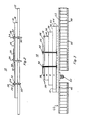
- the capacitively coupled microstrip patch antenna 10 comprises a groundplane 12, dielectric 14 ( Figure 2), antenna element or patch 16 (Figure 1) and capacitively coupled feed lines 18, 20, 22 and 24.
- the groundplane 12 may be, for example, a copper or aluminum sheet and the dielectric layer may be, for example, a Teflon (Trade Mark) fiberglass substrate sold by the 3 M company.
- the antenna element 16 is, for example, a layer of copper formed on the dielectric.
- the capacitively coupled feed lines 18, 20, 22 and 24 each comprise an open electric circuit formed by a dielectric layer (an insulator) 26 over the patch 16 upon which the open circuit elements 28 (flags) are formed.
- Feed pins 30 pass through clearance holes 32 of the patch 16 and are soldered or wire bonded by leads 34 to the open circuit elements 28.
- the patch is electrically isolated from the feed pin.
- a second embodiment of the invention consists of a multilayered patch antenna. Additional antenna elements (patches) 36 and 40 are separated by a dielectric layer 38. Patches 36 and 40 act as groundplanes, respectively, for the antenna elements 16 and 36. Patch 40 is separated from a hybrid feed circuit 44 by a dielectric layer 42.
- the hybrid circuit 44 which is itself a stripline package, is located upon a metal clad mounting 60.
- the hybrid circuit is an out-of-phase power divider providing, for our example, equal power 0, 90,180, and 270 degrees out of phase to conductive pins 18, 20, 22 and 24. Alignment of the hybrid circuit 44 and the mounting 60 is accomplished by alignment pins 46.
- the metal clad mounting 60 is a copper clad fiberglass layer 62 mounted upon a honeycomb substrate 48 mounted upon a mounting plate 50.
- the mounting plate 50 may be, for example, a fiberglass plate.
- the fiberglass layer 62, honeycomb substrate 48 and mounting plate 50 form a light weight strongback mounting having an aperture for an output terminal 52.
- lambda the effective wavelength at the operating frequency.
- the impedance approaches zero ohms. For lengths less than 1/4 lambda, the impedance becomes capacitive.
- the microstrip patch utilizing a rear pin feed inherently has an inductive impedance owing to the length of the pin.
- the inductive reactance of the feed pins 30 is offset by the length of their flags 28 ( Figure 1). In the initial design tuning is accomplished by trimming the length of the flags. This method of feeding is especially effective as it allows a variable capacitance to be introduced which cancels out the inductance of the feed pin. With an antenna as described herein a 1.1 to 1.5 voltage standing wave ratio (VSWR) with maximum gain can be readily obtained.
- VSWR voltage standing wave ratio
- the dimensions of the patches 16, 36 and 40 determine their frequencies. For example, in a global positioning system (GPS) with a nuclear detonation detection information function, the patches 16, 36 and 40 have frequencies of 1575 MHz, 1381 MHz and 1227 MHz, respectively.
- the 1575 and 1227 MHz frequencies of patches 16 and 40 are the GPS position determining frequencies and the 1381 frequency of patch 36 is the frequency of transmission used by nuclear detection systems.
- Any number of the multilayer patch antennas can be combined in a system ( Figure 4), for example, in the Ground/Airborne IGS Terminal twenty-eight such antennas are used.
Landscapes
- Waveguide Aerials (AREA)
Claims (9)
Applications Claiming Priority (2)
| Application Number | Priority Date | Filing Date | Title |
|---|---|---|---|
| US683217 | 1984-12-18 | ||
| US06/683,217 US4660048A (en) | 1984-12-18 | 1984-12-18 | Microstrip patch antenna system |
Publications (2)
| Publication Number | Publication Date |
|---|---|
| EP0188087A1 EP0188087A1 (fr) | 1986-07-23 |
| EP0188087B1 true EP0188087B1 (fr) | 1990-09-26 |
Family
ID=24743053
Family Applications (1)
| Application Number | Title | Priority Date | Filing Date |
|---|---|---|---|
| EP85308987A Expired EP0188087B1 (fr) | 1984-12-18 | 1985-12-11 | Système d'antennes à microbandes |
Country Status (3)
| Country | Link |
|---|---|
| US (1) | US4660048A (fr) |
| EP (1) | EP0188087B1 (fr) |
| JP (1) | JPH0642609B2 (fr) |
Cited By (1)
| Publication number | Priority date | Publication date | Assignee | Title |
|---|---|---|---|---|
| US7489280B2 (en) | 2004-07-20 | 2009-02-10 | Receptec Gmbh | Antenna module |
Families Citing this family (43)
| Publication number | Priority date | Publication date | Assignee | Title |
|---|---|---|---|---|
| US4835539A (en) * | 1986-05-20 | 1989-05-30 | Ball Corporation | Broadbanded microstrip antenna having series-broadbanding capacitance integral with feedline connection |
| US4827271A (en) * | 1986-11-24 | 1989-05-02 | Mcdonnell Douglas Corporation | Dual frequency microstrip patch antenna with improved feed and increased bandwidth |
| US6181277B1 (en) * | 1987-04-08 | 2001-01-30 | Raytheon Company | Microstrip antenna |
| US4924236A (en) * | 1987-11-03 | 1990-05-08 | Raytheon Company | Patch radiator element with microstrip balian circuit providing double-tuned impedance matching |
| DE3738513A1 (de) * | 1987-11-13 | 1989-06-01 | Dornier System Gmbh | Mikrostreifenleiterantenne |
| US5121127A (en) * | 1988-09-30 | 1992-06-09 | Sony Corporation | Microstrip antenna |
| US4932420A (en) * | 1988-10-07 | 1990-06-12 | Clini-Therm Corporation | Non-invasive quarter wavelength microwave applicator for hyperthermia treatment |
| CA2001013C (fr) * | 1988-10-19 | 1995-04-18 | Toshikiyo Hirata | Antenne de reseau |
| FI81927C (fi) * | 1988-10-26 | 1990-12-10 | Nokia Mobira Oy | Antenn foer radiotelefon. |
| US5165109A (en) * | 1989-01-19 | 1992-11-17 | Trimble Navigation | Microwave communication antenna |
| US4980694A (en) * | 1989-04-14 | 1990-12-25 | Goldstar Products Company, Limited | Portable communication apparatus with folded-slot edge-congruent antenna |
| FR2648626B1 (fr) * | 1989-06-20 | 1991-08-23 | Alcatel Espace | Element rayonnant diplexant |
| US5075691A (en) * | 1989-07-24 | 1991-12-24 | Motorola, Inc. | Multi-resonant laminar antenna |
| US4973972A (en) * | 1989-09-07 | 1990-11-27 | The United States Of America As Represented By The Administrator Of The National Aeronautics And Space Adminstration | Stripline feed for a microstrip array of patch elements with teardrop shaped probes |
| US5184141A (en) * | 1990-04-05 | 1993-02-02 | Vought Aircraft Company | Structurally-embedded electronics assembly |
| US5245745A (en) * | 1990-07-11 | 1993-09-21 | Ball Corporation | Method of making a thick-film patch antenna structure |
| US5153600A (en) * | 1991-07-01 | 1992-10-06 | Ball Corporation | Multiple-frequency stacked microstrip antenna |
| US5307075A (en) * | 1991-12-12 | 1994-04-26 | Allen Telecom Group, Inc. | Directional microstrip antenna with stacked planar elements |
| CA2117223A1 (fr) * | 1993-06-25 | 1994-12-26 | Peter Mailandt | Antenne a reseau de plaques microruban |
| US5408241A (en) * | 1993-08-20 | 1995-04-18 | Ball Corporation | Apparatus and method for tuning embedded antenna |
| US5502451A (en) * | 1994-07-29 | 1996-03-26 | The United States Of America As Represented By The Secretary Of The Air Force | Patch antenna with magnetically controllable radiation polarization |
| FR2726127B1 (fr) * | 1994-10-19 | 1996-11-29 | Asulab Sa | Antenne miniaturisee a convertir une tension alternative a une micro-onde et vice-versa, notamment pour des applications horlogeres |
| US5561435A (en) * | 1995-02-09 | 1996-10-01 | The United States Of America As Represented By The Secretary Of The Army | Planar lower cost multilayer dual-band microstrip antenna |
| US5815119A (en) * | 1996-08-08 | 1998-09-29 | E-Systems, Inc. | Integrated stacked patch antenna polarizer circularly polarized integrated stacked dual-band patch antenna |
| US5933121A (en) * | 1998-04-07 | 1999-08-03 | Harris Corporation | Antenna array for sensing signals on conductors |
| GB2352091B (en) * | 1999-07-10 | 2003-09-17 | Alan Dick & Company Ltd | Patch antenna |
| SE517218C2 (sv) * | 1999-09-03 | 2002-05-07 | Ericsson Telefon Ab L M | En lågprofilantennstruktur samt en anordning innefattande trådlöst kommunikationsmedel, en trådlös mobil terminal, ett datorkort lämpligt för införande i en elektronisk anordning och ett lokalt nätverkssystem innefattande en basstation och ett flertal terminaler vilka är i trådlös kommunikation med basstationen innefattande en sådan lågprofilantennstruktur |
| US6448924B1 (en) * | 1999-10-12 | 2002-09-10 | Smiths Aerospace, Inc. | Microwave blade tracker |
| US6778144B2 (en) | 2002-07-02 | 2004-08-17 | Raytheon Company | Antenna |
| DE60222308D1 (de) * | 2002-10-25 | 2007-10-18 | Nat Inst Inf & Comm Tech | Antennenvorrichtung |
| JP2004165980A (ja) * | 2002-11-13 | 2004-06-10 | Alps Electric Co Ltd | パッチアンテナ |
| EP1911090A4 (fr) * | 2005-07-29 | 2009-07-22 | Foster Miller Inc | Systeme composite bifoncitonnel et procede de fabrication |
| JP4678351B2 (ja) * | 2006-09-05 | 2011-04-27 | 三菱電機株式会社 | アンテナ装置 |
| US7692592B2 (en) * | 2008-07-24 | 2010-04-06 | The United States Of America As Represented By The Secretary Of The Army | High power two-patch array antenna system |
| JP5153522B2 (ja) * | 2008-09-01 | 2013-02-27 | 三菱電機株式会社 | アンテナ装置、及びアレーアンテナ装置 |
| GB2517852A (en) * | 2012-04-05 | 2015-03-04 | Tallysman Wireless Inc | Capacitively coupled patch antenna |
| US10992058B2 (en) * | 2012-04-05 | 2021-04-27 | Tallysman Wireless Inc. | Capacitively coupled patch antenna |
| US10553951B2 (en) * | 2012-04-05 | 2020-02-04 | Tallysman Wireless Inc. | Capacitively coupled patch antenna |
| US10950944B2 (en) * | 2012-04-05 | 2021-03-16 | Tallysman Wireless Inc. | Capacitively coupled patch antenna |
| JP2018056937A (ja) * | 2016-09-30 | 2018-04-05 | 沖電気工業株式会社 | パッチアンテナ組立体およびパッチアンテナ |
| WO2020217971A1 (fr) | 2019-04-24 | 2020-10-29 | 株式会社村田製作所 | Module d'antenne et dispositif de communication équipé de celui-ci |
| US11544517B2 (en) * | 2020-10-03 | 2023-01-03 | MHG IP Holdings, LLC | RFID antenna |
| CN121076464A (zh) * | 2024-06-05 | 2025-12-05 | 华为技术有限公司 | 一种天线 |
Family Cites Families (13)
| Publication number | Priority date | Publication date | Assignee | Title |
|---|---|---|---|---|
| US2998605A (en) * | 1957-07-09 | 1961-08-29 | Hazeltine Research Inc | Antenna system |
| US3016536A (en) * | 1958-05-14 | 1962-01-09 | Eugene G Fubini | Capacitively coupled collinear stripline antenna array |
| US3665480A (en) | 1969-01-23 | 1972-05-23 | Raytheon Co | Annular slot antenna with stripline feed |
| US4054874A (en) * | 1975-06-11 | 1977-10-18 | Hughes Aircraft Company | Microstrip-dipole antenna elements and arrays thereof |
| US4070676A (en) * | 1975-10-06 | 1978-01-24 | Ball Corporation | Multiple resonance radio frequency microstrip antenna structure |
| US4218682A (en) * | 1979-06-22 | 1980-08-19 | Nasa | Multiple band circularly polarized microstrip antenna |
| US4364050A (en) * | 1981-02-09 | 1982-12-14 | Hazeltine Corporation | Microstrip antenna |
| US4443802A (en) | 1981-04-22 | 1984-04-17 | University Of Illinois Foundation | Stripline fed hybrid slot antenna |
| FR2505097A1 (fr) * | 1981-05-04 | 1982-11-05 | Labo Electronique Physique | Element rayonnant ou recepteur de signaux hyperfrequences a polarisations circulaires et antenne plane hyperfrequence comprenant un reseau de tels elements |
| JPS5916402A (ja) * | 1982-07-19 | 1984-01-27 | Nippon Telegr & Teleph Corp <Ntt> | 2周波共用広帯域マイクロストリツプアンテナ |
| US4477813A (en) * | 1982-08-11 | 1984-10-16 | Ball Corporation | Microstrip antenna system having nonconductively coupled feedline |
| JPS59181706A (ja) * | 1983-03-30 | 1984-10-16 | Radio Res Lab | マイクロストリツプアンテナ |
| US4605932A (en) * | 1984-06-06 | 1986-08-12 | The United States Of America As Represented By The Secretary Of The Navy | Nested microstrip arrays |
-
1984
- 1984-12-18 US US06/683,217 patent/US4660048A/en not_active Expired - Lifetime
-
1985
- 1985-12-11 EP EP85308987A patent/EP0188087B1/fr not_active Expired
- 1985-12-18 JP JP60285382A patent/JPH0642609B2/ja not_active Expired - Lifetime
Cited By (1)
| Publication number | Priority date | Publication date | Assignee | Title |
|---|---|---|---|---|
| US7489280B2 (en) | 2004-07-20 | 2009-02-10 | Receptec Gmbh | Antenna module |
Also Published As
| Publication number | Publication date |
|---|---|
| JPS61146003A (ja) | 1986-07-03 |
| EP0188087A1 (fr) | 1986-07-23 |
| US4660048A (en) | 1987-04-21 |
| JPH0642609B2 (ja) | 1994-06-01 |
Similar Documents
| Publication | Publication Date | Title |
|---|---|---|
| EP0188087B1 (fr) | Système d'antennes à microbandes | |
| US4401988A (en) | Coupled multilayer microstrip antenna | |
| US6281843B1 (en) | Planar broadband dipole antenna for linearly polarized waves | |
| US4475108A (en) | Electronically tunable microstrip antenna | |
| JP3093715B2 (ja) | 共振器付着型マイクロストリップダイポールアンテナアレイ | |
| US4477813A (en) | Microstrip antenna system having nonconductively coupled feedline | |
| EP0720252B1 (fr) | Antenne miniature à microbande à branches multiples | |
| US6091373A (en) | Feed device for a radiating element operating in dual polarization | |
| US4040060A (en) | Notch fed magnetic microstrip dipole antenna with shorting pins | |
| US4054874A (en) | Microstrip-dipole antenna elements and arrays thereof | |
| US4812855A (en) | Dipole antenna with parasitic elements | |
| US5786793A (en) | Compact antenna for circular polarization | |
| US4125839A (en) | Dual diagonally fed electric microstrip dipole antennas | |
| EP0176311B1 (fr) | Mini-antenne | |
| US3971032A (en) | Dual frequency microstrip antenna structure | |
| US4847625A (en) | Wideband, aperture-coupled microstrip antenna | |
| US4710775A (en) | Parasitically coupled, complementary slot-dipole antenna element | |
| US4320402A (en) | Multiple ring microstrip antenna | |
| US4083046A (en) | Electric monomicrostrip dipole antennas | |
| US3803623A (en) | Microstrip antenna | |
| EP0343322A2 (fr) | Antenne fente à alimentation microbande | |
| US5444452A (en) | Dual frequency antenna | |
| EP3526855B1 (fr) | Antenne double bande à ouverture partagée à couche unique | |
| EP0001883A1 (fr) | Système de découplage de réseaux de microstrip antennes adjacentes | |
| US4078237A (en) | Offset FED magnetic microstrip dipole antenna |
Legal Events
| Date | Code | Title | Description |
|---|---|---|---|
| PUAI | Public reference made under article 153(3) epc to a published international application that has entered the european phase |
Free format text: ORIGINAL CODE: 0009012 |
|
| AK | Designated contracting states |
Kind code of ref document: A1 Designated state(s): FR GB |
|
| 17P | Request for examination filed |
Effective date: 19861218 |
|
| 17Q | First examination report despatched |
Effective date: 19880719 |
|
| GRAA | (expected) grant |
Free format text: ORIGINAL CODE: 0009210 |
|
| AK | Designated contracting states |
Kind code of ref document: B1 Designated state(s): FR GB |
|
| ET | Fr: translation filed | ||
| PLBE | No opposition filed within time limit |
Free format text: ORIGINAL CODE: 0009261 |
|
| STAA | Information on the status of an ep patent application or granted ep patent |
Free format text: STATUS: NO OPPOSITION FILED WITHIN TIME LIMIT |
|
| 26N | No opposition filed | ||
| REG | Reference to a national code |
Ref country code: GB Ref legal event code: 732E |
|
| REG | Reference to a national code |
Ref country code: FR Ref legal event code: TP |
|
| REG | Reference to a national code |
Ref country code: GB Ref legal event code: 732E |
|
| REG | Reference to a national code |
Ref country code: FR Ref legal event code: TP |
|
| PGFP | Annual fee paid to national office [announced via postgrant information from national office to epo] |
Ref country code: FR Payment date: 19991217 Year of fee payment: 15 |
|
| PGFP | Annual fee paid to national office [announced via postgrant information from national office to epo] |
Ref country code: GB Payment date: 19991224 Year of fee payment: 15 |
|
| PG25 | Lapsed in a contracting state [announced via postgrant information from national office to epo] |
Ref country code: GB Free format text: LAPSE BECAUSE OF NON-PAYMENT OF DUE FEES Effective date: 20001211 |
|
| GBPC | Gb: european patent ceased through non-payment of renewal fee |
Effective date: 20001211 |
|
| PG25 | Lapsed in a contracting state [announced via postgrant information from national office to epo] |
Ref country code: FR Free format text: LAPSE BECAUSE OF NON-PAYMENT OF DUE FEES Effective date: 20010831 |
|
| REG | Reference to a national code |
Ref country code: FR Ref legal event code: ST |