EP0188444B1 - Contacts electriques comprenant un alliage de palladium et connecteurs composes de ces contacts - Google Patents
Contacts electriques comprenant un alliage de palladium et connecteurs composes de ces contacts Download PDFInfo
- Publication number
- EP0188444B1 EP0188444B1 EP19850902808 EP85902808A EP0188444B1 EP 0188444 B1 EP0188444 B1 EP 0188444B1 EP 19850902808 EP19850902808 EP 19850902808 EP 85902808 A EP85902808 A EP 85902808A EP 0188444 B1 EP0188444 B1 EP 0188444B1
- Authority
- EP
- European Patent Office
- Prior art keywords
- alloy
- contact according
- layer
- weight percent
- base metal
- Prior art date
- Legal status (The legal status is an assumption and is not a legal conclusion. Google has not performed a legal analysis and makes no representation as to the accuracy of the status listed.)
- Expired
Links
- 229910001252 Pd alloy Inorganic materials 0.000 title claims abstract description 16
- 229910045601 alloy Inorganic materials 0.000 claims abstract description 72
- 239000000956 alloy Substances 0.000 claims abstract description 72
- 239000010953 base metal Substances 0.000 claims abstract description 38
- KDLHZDBZIXYQEI-UHFFFAOYSA-N palladium Substances [Pd] KDLHZDBZIXYQEI-UHFFFAOYSA-N 0.000 claims abstract description 18
- 229910052796 boron Inorganic materials 0.000 claims abstract description 15
- 229910052802 copper Inorganic materials 0.000 claims abstract description 14
- 229910052727 yttrium Inorganic materials 0.000 claims abstract description 11
- 229910052741 iridium Inorganic materials 0.000 claims abstract description 9
- 229910052758 niobium Inorganic materials 0.000 claims abstract description 5
- PXHVJJICTQNCMI-UHFFFAOYSA-N Nickel Chemical compound [Ni] PXHVJJICTQNCMI-UHFFFAOYSA-N 0.000 claims description 45
- 229910052751 metal Inorganic materials 0.000 claims description 32
- 239000002184 metal Substances 0.000 claims description 32
- 229910052759 nickel Inorganic materials 0.000 claims description 22
- PCHJSUWPFVWCPO-UHFFFAOYSA-N gold Chemical compound [Au] PCHJSUWPFVWCPO-UHFFFAOYSA-N 0.000 claims description 19
- 229910052737 gold Inorganic materials 0.000 claims description 19
- 239000010931 gold Substances 0.000 claims description 19
- 238000000137 annealing Methods 0.000 claims description 13
- 239000010949 copper Substances 0.000 claims description 13
- 239000000203 mixture Substances 0.000 claims description 11
- 238000009792 diffusion process Methods 0.000 claims description 7
- ZOXJGFHDIHLPTG-UHFFFAOYSA-N Boron Chemical compound [B] ZOXJGFHDIHLPTG-UHFFFAOYSA-N 0.000 claims description 4
- 239000010955 niobium Substances 0.000 claims description 4
- 229910052709 silver Inorganic materials 0.000 claims description 4
- 229910001316 Ag alloy Inorganic materials 0.000 claims description 3
- 229910001020 Au alloy Inorganic materials 0.000 claims description 3
- 239000003353 gold alloy Substances 0.000 claims description 3
- 150000001247 metal acetylides Chemical class 0.000 claims description 3
- 150000004767 nitrides Chemical class 0.000 claims description 3
- 239000004332 silver Substances 0.000 claims description 3
- 229910052582 BN Inorganic materials 0.000 claims description 2
- PZNSFCLAULLKQX-UHFFFAOYSA-N Boron nitride Chemical compound N#B PZNSFCLAULLKQX-UHFFFAOYSA-N 0.000 claims description 2
- OKTJSMMVPCPJKN-UHFFFAOYSA-N Carbon Chemical compound [C] OKTJSMMVPCPJKN-UHFFFAOYSA-N 0.000 claims description 2
- 229910052799 carbon Inorganic materials 0.000 claims description 2
- MZLGASXMSKOWSE-UHFFFAOYSA-N tantalum nitride Chemical compound [Ta]#N MZLGASXMSKOWSE-UHFFFAOYSA-N 0.000 claims description 2
- MTPVUVINMAGMJL-UHFFFAOYSA-N trimethyl(1,1,2,2,2-pentafluoroethyl)silane Chemical compound C[Si](C)(C)C(F)(F)C(F)(F)F MTPVUVINMAGMJL-UHFFFAOYSA-N 0.000 claims description 2
- 239000010410 layer Substances 0.000 description 59
- 239000000463 material Substances 0.000 description 12
- 238000005253 cladding Methods 0.000 description 10
- 238000005096 rolling process Methods 0.000 description 9
- 229910052763 palladium Inorganic materials 0.000 description 7
- 241000242599 Tricladida Species 0.000 description 6
- 229910017052 cobalt Inorganic materials 0.000 description 6
- 239000010941 cobalt Substances 0.000 description 6
- 229910001092 metal group alloy Inorganic materials 0.000 description 6
- 229910052707 ruthenium Inorganic materials 0.000 description 6
- RYGMFSIKBFXOCR-UHFFFAOYSA-N Copper Chemical compound [Cu] RYGMFSIKBFXOCR-UHFFFAOYSA-N 0.000 description 5
- GUTLYIVDDKVIGB-UHFFFAOYSA-N cobalt atom Chemical compound [Co] GUTLYIVDDKVIGB-UHFFFAOYSA-N 0.000 description 5
- KJTLSVCANCCWHF-UHFFFAOYSA-N Ruthenium Chemical group [Ru] KJTLSVCANCCWHF-UHFFFAOYSA-N 0.000 description 4
- 238000005336 cracking Methods 0.000 description 4
- 238000000034 method Methods 0.000 description 4
- 239000000654 additive Substances 0.000 description 3
- 150000002739 metals Chemical class 0.000 description 3
- 238000001953 recrystallisation Methods 0.000 description 3
- 229910002058 ternary alloy Inorganic materials 0.000 description 3
- 229910001369 Brass Inorganic materials 0.000 description 2
- 229910000881 Cu alloy Inorganic materials 0.000 description 2
- 229910018100 Ni-Sn Inorganic materials 0.000 description 2
- 229910018532 Ni—Sn Inorganic materials 0.000 description 2
- BQCADISMDOOEFD-UHFFFAOYSA-N Silver Chemical compound [Ag] BQCADISMDOOEFD-UHFFFAOYSA-N 0.000 description 2
- 229910001128 Sn alloy Inorganic materials 0.000 description 2
- 230000000996 additive effect Effects 0.000 description 2
- 239000010951 brass Substances 0.000 description 2
- 230000001680 brushing effect Effects 0.000 description 2
- 238000004140 cleaning Methods 0.000 description 2
- 239000011248 coating agent Substances 0.000 description 2
- 238000000576 coating method Methods 0.000 description 2
- 239000002131 composite material Substances 0.000 description 2
- 239000000470 constituent Substances 0.000 description 2
- 238000005260 corrosion Methods 0.000 description 2
- 230000007797 corrosion Effects 0.000 description 2
- 230000000694 effects Effects 0.000 description 2
- PQTCMBYFWMFIGM-UHFFFAOYSA-N gold silver Chemical compound [Ag].[Au] PQTCMBYFWMFIGM-UHFFFAOYSA-N 0.000 description 2
- 238000004519 manufacturing process Methods 0.000 description 2
- 229910000510 noble metal Inorganic materials 0.000 description 2
- BASFCYQUMIYNBI-UHFFFAOYSA-N platinum Chemical compound [Pt] BASFCYQUMIYNBI-UHFFFAOYSA-N 0.000 description 2
- 229910000679 solder Inorganic materials 0.000 description 2
- 239000010935 stainless steel Substances 0.000 description 2
- 229910001220 stainless steel Inorganic materials 0.000 description 2
- 239000002344 surface layer Substances 0.000 description 2
- 229910052721 tungsten Inorganic materials 0.000 description 2
- WFKWXMTUELFFGS-UHFFFAOYSA-N tungsten Chemical compound [W] WFKWXMTUELFFGS-UHFFFAOYSA-N 0.000 description 2
- 239000010937 tungsten Substances 0.000 description 2
- 238000003466 welding Methods 0.000 description 2
- 229910000531 Co alloy Inorganic materials 0.000 description 1
- 229910020514 Co—Y Inorganic materials 0.000 description 1
- 229910017532 Cu-Be Inorganic materials 0.000 description 1
- 229910000990 Ni alloy Inorganic materials 0.000 description 1
- 229910000929 Ru alloy Inorganic materials 0.000 description 1
- 230000004888 barrier function Effects 0.000 description 1
- 229910052790 beryllium Inorganic materials 0.000 description 1
- 230000015572 biosynthetic process Effects 0.000 description 1
- 238000005266 casting Methods 0.000 description 1
- 239000000356 contaminant Substances 0.000 description 1
- 238000005520 cutting process Methods 0.000 description 1
- 230000001419 dependent effect Effects 0.000 description 1
- 239000012535 impurity Substances 0.000 description 1
- GKOZUEZYRPOHIO-UHFFFAOYSA-N iridium atom Chemical compound [Ir] GKOZUEZYRPOHIO-UHFFFAOYSA-N 0.000 description 1
- 239000000314 lubricant Substances 0.000 description 1
- 238000005461 lubrication Methods 0.000 description 1
- 230000013011 mating Effects 0.000 description 1
- 239000000155 melt Substances 0.000 description 1
- 238000002844 melting Methods 0.000 description 1
- 230000008018 melting Effects 0.000 description 1
- GUCVJGMIXFAOAE-UHFFFAOYSA-N niobium atom Chemical compound [Nb] GUCVJGMIXFAOAE-UHFFFAOYSA-N 0.000 description 1
- 238000007747 plating Methods 0.000 description 1
- 229910052697 platinum Inorganic materials 0.000 description 1
- 239000010970 precious metal Substances 0.000 description 1
- 238000004544 sputter deposition Methods 0.000 description 1
- 239000000126 substance Substances 0.000 description 1
Images


Classifications
-
- H—ELECTRICITY
- H01—ELECTRIC ELEMENTS
- H01H—ELECTRIC SWITCHES; RELAYS; SELECTORS; EMERGENCY PROTECTIVE DEVICES
- H01H1/00—Contacts
- H01H1/02—Contacts characterised by the material thereof
- H01H1/021—Composite material
- H01H1/023—Composite material having a noble metal as the basic material
Definitions
- This invention relates to electrical contacts useful in connectors as well as other applications, such as in voltage regulators, relays and switches.
- the composition should be non-fusing with the mating contact material and have a low, ohmic, contact resistance with a relatively small contact pressure.
- the material must be capable of maintaining the low resistance after a large number of operations over an extended life period.
- the contact materials employed in the past are the precious metals such as gold, palladium and platinum and alloys of such metals with each other as well as with metals such as silver and nickel. It is often found that the contact or connector is multi-layer or inlayed type structure.
- a gold-palladium-silver based alloy has been developed for use as an inlay in contact connector applications.
- the inlay comprises a relatively inexpensive base metal strip having a channel cut out of the strip into which channel has been inlayed the desired contact metal alloy.
- Typical base metals are copper, brass, Cu-Be and Cu-Ni-Sn alloys, as well as stainless steel and other spring metal alloys.
- R156 40% silver-60% palladium alloy
- This alloy may be used either with or without a diffused gold layer on its surface.
- This and other prior art alloys exhibit limited wear behavior and are generally relatively high in cost.
- This invention is an electrical contact suitable for use in connectors and other devices such as relays, switches, voltage regulators and the like comprises a base metal having a palladium alloy thereon represented by the composition:
- the alloy may be in the form of a multi-layer metal tape comprising said alloy which tape can be clad to or inlayed in a base metal to form a contact.
- the contact alloys embodying the present invention generally exhibit improved wear characteristics due to an increase in hardness, but yet still exhibit sufficient ductility for use in metal cladding, inlaying or welding to a base metal for electrical contact applications. Further these alloys generally have superior wear chanracteris- tics, they can be used in thinner layers than prior art noble metal alloys, thereby reducing the cost of the contact and connector or other device employing these alloys. In addition, since a large part of the alloy is comprised of a non-noble metal, the cost of the alloy even at the same thickness as prior art alloys is reduced.
- the electrical contacts embodying this invention which may be employed in connectors and other electrical devices requiring electrical contacts, are comprised of a hardened palladium alloy.
- the alloy composition is generally present as an inlay, cladding or other type coating over at least a portion of a base metal forming the electrical contact.
- the alloys may be one layer of a multilayer tape. Such a tape can then be used for cladding, bonding, welding or inlaying to a base metal.
- Such base metals are typically metals such as copper, brass, copper-beryllium and copper-nickel-tin-alloys as well as stainless steel or other spring metal alloys.
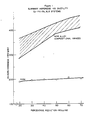
- the alloys are suitable for use either with or without gold or gold alloy top layers. Based upon the improved hardness and ductility of the novel alloys as compared with the currently employed commercial R156 alloy, it is expected that contacts made from these novel alloys will also have superior wear properties. It is contemplated that the new alloys are particularly suitable as an inlay material and therefore their ability to be rolled without cracking, i.e., their ductility, is important to the formation of such metal inlays or of cladded contacts. Also, the recrystallization behavior and ductility of the new alloys which are important to metal inlaying or cladding art at least equal to that of the prior art alloy.
- ductility as measured by percentage deformation by rolling without cracking versus the Vickers hardness of Pd-Co-Y alloys wherein Y is Ru, W or B, one of the alloy systems in accordance with the present invention, is shown in comparison to the prior art R156 alloy. It can be seen that for any given ductility i.e, percentage reduction in thickness by rolling, the new alloys generally have a higher Vickers hardness than R156. Correspondingly, for any given Vickers hardness the new alloys are more ductile than the prior art alloy.
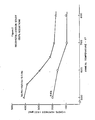
- the Vickers hardness of the novel alloy is greater than that of the referenced prior art alloy at any given anneal temperature.
- the particular novel alloy shown in fact, has a lower hardness than novel alloys with more Ru as well as many other alloys included in the claimed alloy systems.
- the preferred additive is ruthenium in a quantity of from 0.5 to 5 weight percent.
- the preferred additive is boron in a weight range of from 0.05 to 0.10 weight percent.
- the ruthenium, tungsten and niobium which are suitable additives to a palladium-cobalt alloy to achieve the desired properties of hardness and ductility, are not as suitable for a palladium-copper alloy due to their relative insolubility in such an alloy and the brittleness of the resulting ternary alloy. Further, in order to achieve the desired combination of hardness and ductility so as to allow the alloyed material to be rolled without cracking, one should stay within the weight percent ranges as previously set forth.
- the preferred amount of tungsten added to the palladium-cobalt system is 0.5 to 2 weight percent, while the preferred amount of boron in that system is 0.1 to 0.26 weight percent.
- the preferred amount of iridium added to a palladium-copper alloy is from 0.25 to 1 weight percent.
- the particular amounts of materials for achieving optimum performance will depend upon the ratio of palladium to cobalt and palladium to copper, respectively.
- Fig. 3 is an example showing the relative brittleness of one of the preferred ternary alloy systems, namely, the palladium-cobalt-ruthenium system. As can be seen from the figure, as one goes above 5 wt. % Ru (outside the ranges set forth herein), the brittleness of the alloy increase above that which is desirable.
- novel alloys can be prepared by simply melting the constituent components together to form a homogeneous molten solution, casting the solution onto an appropriate mold and then allowing the solution to cool so as to solidify the melt.
- a laminar structure metal tape 1 comprising the novel alloy as one of the layers.
- This tape is particularly suitable for cladding to or inlaying in a base metal such as a spring metal alloy base metal.
- the tape 1 comprises three layers.
- the top layer 2 is made of either a gold or gold-silver or gold-silver alloy doped further with carbon, carbides, nitrides, boron or borides. Examples of suitable nitrides, carbides and borides are boron nitride, titanium carbide and tantalum nitride.
- the top layer 2 When the top layer 2 is to act as an inert surface layer to inhibit corrosion, that layer should generally be between 1.27x10- 5 cm to 7.62x10- 5 cm (5 microinches to 30 microinches thick. Such a layer is generally termed a gold cap layer. Alternatively, one can also make the top layer 2 a flash gold coating which acts predominantly as a lubricant while only giving miniamal corrosion resistance. Such layers are generally from 1.27x10- 6 to 6.35x10- s cm (0.5 to 2.5 microinches in thickness.
- the second layer 4 of the tape 1 is a layer of the novel alloy as set forth herein. The preferred alloy for such a tape is 65 wt. % Co, 33 wt. % Pd and 2. wt. % Ru.
- this second layer 4 is from 3.81 x 10- 5 cm to 5.08x 10- 4 cm (15 to 200 microinches) in thickness.
- a bottom layer 6 made of nickel.
- the nickel should be a high purity nickel (99.9+%) so as not to add contaminants to the second layer 4 upon annealing.
- the thickness of the nickel layer 6 may be any desired thickness, but is typically from 3.81 x10- 4 cm to 11.43x10- 4 cm (150 to 450 microinches).
- the nickel layer 6 serves several purposes. First, the nickel layer 6 acts as a base material for the thin gold cap and palladium alloy layers. Secondly, the nickel layer 6 enhances the bondability of the tape 1 to the underlying base metal material.
- a fourth layer (not shown) between the palladium alloy layer 4 and the bottom nickel layer 6 to further insure that the ruthenium and cobalt or the like in the palladium alloy layer 4 does not diffuse into the nickel layer and underlaying base metal.
- This optional layer is preferably a thin silver layer of a thin layer of silver alloy.
- one can bond the novel alloy directly to a base metal, the tri-layer structure merely being the more generally preferred structure for a tape to be clad or inlayed to a base metal.
- the tape is annealed typically at temperatures of from 600°C to 850°C for times of from 0.5 to 60 minutes. During such annealing, there is a diffusion of constituents between layers and the relative hardness as well as the composition of the layers is effected.
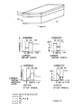
- Fig. 5 there is depicted the relative hardness and chemistry of each of the three layers 2, 4 and 6 before annealing and then again after annealing of a Pd-Cu-Ru alloy, showing the change in hardness and chemistry of the layers due to annealing.
- the chemistry of the layers changes upon annealing due to the diffusion of some of the gold into the underlying palladium alloy layer 4 and some of the palladium diffusing into the gold layer 2. Diffusion into the underlaying nickel layer 6 which acts as a diffusion barrier for components in the base metal strip, is not considered. Further, there is only minimal diffusion of ruthenium and cobalt into the gold layer 2 from the Pd alloy layer 4.
- the Co is believed not to effectively diffuse into the gold layer beyond the equilibrium Co in gold concentration which may be controlled by the annealing temperature.
- the hardness With respect to the hardness, a change in the hardness profile can be seen partially due to the diffusion and partially due simply to the effects of the annealing temperature.
- FIG. 6 there is shown a connector 10 incorporating a contact 14 which employs the novel alloy and metal tape 1 made from such alloy.
- Fig. 7 is a blow-up of the contact 14 portion of the connector 10.
- the connector 10 as shown, comprises a plastic body 12 encasing a plurality of spaced external elongated contacts 14 for interconnecting the connector 10 to various other devices or ciruits.
- the contacts 14 are embedded within cavities provided therefor within the plastic terminal block or insulating body 12.
- the contacts 14 have a solder coated tail 16 which extends out of the body 12 and a head portion 18 having a multilayer metal alloy tape 1 inlayed therein.
- the contacts 14 extend transversely within the connector 10 and are registered with a port or hole 22 on the side of the connector 10 or opposite the contact tail 16 for accepting a connector pin 24, e.g., from another circuit source.
- the contact 14 is better shown with the reference to Fig. 7 which shows a side view of a connector contact 14.
- the base 20 of the contact 14 is made primarily of a resilient or spring alloy composition, e.g., a Cu/Ni/Sn alloy.
- Extending transversely along the tip of the head 18 of the contact 14 is the metal inlay tape 1.
- the inlay tape 1 is a tri-layer tape as previously described with reference to Fig. 4. This tape 1 was rolled bonded into a channel scribed in the base metal. The base metal was then punched and formed as is well known in the art to result in the connector contact shown.
- the manufacture of the triclad tape starts with metal strips of each material to be bonded together, i.e., gold, novel alloy and nickel whose thickness represent the general thickness ratio of the final composite tape.
- the surfaces of the metal strips to be bonded are degreased, cleaned and scratch brushed to roughen the surfaces in order to improve the bonding capabilities. the scratch brushed surfaces are then recleaned to remove debris from the scratch brushing operation.
- the triclad tape can be manufactured in one step by alignement of the three strips stacked in the appropriate sequence and roll bonded together.
- Each strip should have a tack tension applied to it as it is being rolled to insure consistent rolling behavior and uniform product thickness.
- the exact layer thickness depends upon the levels of back and front tensions, strip initial thickness, strip material, percentage of deformation, use of lubrication, rolling pressure and amount of slippage between strips.
- the triclad tape can be manufactured in two steps by first bonding one pair of metal strips, i.e., the gold and hardened palladium alloy, and then bonding the bi-metal strip to the nickel.
- metal strips i.e., the gold and hardened palladium alloy
- the bi-metal strip to the nickel.
- a minimum reduction in thickness is required to achieve any bonding between two metal strips and the required minimum amount is a function of the metal (alloys) and rolling temperatures.
- a gold strip to the novel alloy a reduction of 45-65% is required.
- a deformation of about 75% reduction or more is required.
- the triclad tape can then be slit into the desired width and cut to length for metal inlaying or cladding to the base metal strip. More than one strip can be inlayed or cladded to a wide base metal strip at one time to allow for production of mulitple strips which may have multiple inlays on its surfaces.
- the novel palladium alloy can be bonded to the nickel strip and the gold surface layer can be applied either before or after inlay- ing/cladding into the base metal strip by plating, sputtering or some other process.
- Annealing the bonded strip is dependent upon the composition of the metal layers. Nickel can be fully annealed at 600°C for 5-15 minutes; the novel palladium alloys can be annealed in the temperature ranges of from 600-850°C.
- the most critical anneal for interdiffusion of elements between metal layers occurs when the layers are in the final base metal strip configuration just prior to the final rolling to achieve the desired temperature in the base metal strip. It is at this point in the processing when interdiffusion between layers is critical due to the very thin layer thicknesses.
- Cladding is typically defined as the operation where metal strips are joined by rolling together while the inlaying process involves cutting or skiving a channel in the base metal in order to incorporate a second metal strip, or in this case, a triclad metal strip containing the novel alloy.
- the metal inlaying process is generally preferred if the location of the second metal strip is critical or if the thickness of the inlay would be a significant proportion of the total thickness of the finished strip (i.e., greater than 15%).
- the cleaning procedures for metal cladding the triclad strip and base metal are identical to those described earlier, whereas for metal inlaying it is not necessary for extensive base metal cleaning or scratch brushing since a new surface will be skived into the strip just prior to bonding.
- the typical reduction to bond the nickel surface to a base metal alloy, i.e., CDA725 (a Cu-Ni-Sn alloy) is between 55-75% reduction with higher bond strength associated with the higher reduction.
- Annealing of the inlayed composite strip is in the range of 600-850°C for the typical novel alloy inlay for 0.5 to 60 minutes to control the interdiffusion of elements.
- the final rolling of the inlayed strip is typically 40-55% reduction to achieve the desired temperature in the (CDA725) base metal.
- the completed base metal strip containing the metal inlay can now be slit to the appropriate width which also accurately locates the position of the inlay in reference to the strip width for ease in stamping.
- the finished strip may be inspected and processed through a stretcher- leveler to reduce strip camber and coil set if it is necessary.
- Other optional processes might include application of a solder top and/or bottom layer for easier assembly of parts.
- the finished strip can then be fed into a high speed punch where the contact is stamped and formed. This is typically a reel-to-reel operation after which the formed contacts are inserted into the plastic housing of the connector and cut from the reel. Finished connectors are then inspected and tested.
Landscapes
- Chemical & Material Sciences (AREA)
- Engineering & Computer Science (AREA)
- Composite Materials (AREA)
- Materials Engineering (AREA)
- Contacts (AREA)
Abstract
Claims (20)
Applications Claiming Priority (2)
| Application Number | Priority Date | Filing Date | Title |
|---|---|---|---|
| US62527484A | 1984-06-27 | 1984-06-27 | |
| US625274 | 2000-07-25 |
Publications (2)
| Publication Number | Publication Date |
|---|---|
| EP0188444A1 EP0188444A1 (fr) | 1986-07-30 |
| EP0188444B1 true EP0188444B1 (fr) | 1989-03-15 |
Family
ID=24505329
Family Applications (1)
| Application Number | Title | Priority Date | Filing Date |
|---|---|---|---|
| EP19850902808 Expired EP0188444B1 (fr) | 1984-06-27 | 1985-05-13 | Contacts electriques comprenant un alliage de palladium et connecteurs composes de ces contacts |
Country Status (3)
| Country | Link |
|---|---|
| EP (1) | EP0188444B1 (fr) |
| DE (1) | DE3568901D1 (fr) |
| WO (1) | WO1986000461A1 (fr) |
Family Cites Families (4)
| Publication number | Priority date | Publication date | Assignee | Title |
|---|---|---|---|---|
| GB1188773A (en) * | 1968-03-25 | 1970-04-22 | Int Nickel Ltd | Ruthenium Alloys. |
| BE770653A (fr) * | 1970-08-06 | 1971-12-01 | Heraeus Gmbh W C | Utilisation d'un alliage de palladium pour des pieces de contact electriques |
| DE2753654C2 (de) * | 1977-12-02 | 1982-12-23 | W.C. Heraeus Gmbh, 6450 Hanau | Legierung aus Palladium, Kobalt und Kupfer für elektrische Kontakte |
| DE3307182A1 (de) * | 1982-05-26 | 1983-12-01 | Technical Materials, Inc., Lincoln, R.I. | Legierung fuer elektrische kontakte und verwendung fuer eine solche legierung |
-
1985
- 1985-05-13 DE DE8585902808T patent/DE3568901D1/de not_active Expired
- 1985-05-13 WO PCT/US1985/000895 patent/WO1986000461A1/fr not_active Ceased
- 1985-05-13 EP EP19850902808 patent/EP0188444B1/fr not_active Expired
Also Published As
| Publication number | Publication date |
|---|---|
| WO1986000461A1 (fr) | 1986-01-16 |
| EP0188444A1 (fr) | 1986-07-30 |
| DE3568901D1 (en) | 1989-04-20 |
Similar Documents
| Publication | Publication Date | Title |
|---|---|---|
| EP2045362A1 (fr) | Matériau plaqué, son procédé de fabrication et pièce électronique l'utilisant | |
| US6755958B2 (en) | Barrier layer for electrical connectors and methods of applying the layer | |
| EP2175460A1 (fr) | Matériau à revêtement argent pour élément de contact mobile et procédé de production | |
| US6495001B2 (en) | Method for manufacturing a metallic composite strip | |
| KR19980033263A (ko) | 단자재료 및 단자 | |
| JP2002339097A (ja) | 近表面をドープしたスズまたはスズ合金で被覆された金属製品 | |
| EP1391969A2 (fr) | Contact ayant une couche de Ruthenium et part l'utilisant | |
| JP2003171790A (ja) | めっき材料とその製造方法、それを用いた電気・電子部品 | |
| US20060204741A1 (en) | Contact surfaces for electrical contacts and method for producing the same | |
| JP2009084616A (ja) | リフローSnめっき材及びそれを用いた電子部品 | |
| US6641930B2 (en) | Electrically conductive metal tape and plug connector | |
| CN100511852C (zh) | 电接触器 | |
| US20050037229A1 (en) | Plated material, method of producing same, and electrical / electronic part using same | |
| US4579787A (en) | Material for low voltage current contacts | |
| EP0188444B1 (fr) | Contacts electriques comprenant un alliage de palladium et connecteurs composes de ces contacts | |
| Lindborg et al. | Intermetallic growth and contact resistance of tin contacts after aging | |
| JP3519726B1 (ja) | 端子およびそれを有する部品 | |
| JP2003328157A (ja) | めっき材料とその製造方法、それを用いた電気・電子部品 | |
| JP2851245B2 (ja) | Sn合金めっき材 | |
| JPH048883B2 (fr) | ||
| CA2069390A1 (fr) | Contacts ou connecteurs electriques anticorrosion haute temperature et methode de fabrication connexe | |
| JPH0711477A (ja) | 貴金属めっき品 | |
| JP3515226B2 (ja) | 銀被覆バネ用りん青銅とその製造方法 | |
| EP0082647A2 (fr) | Contacts à courant faible, résistant à la corrosion | |
| EP0084161A2 (fr) | Cadres de connexion pour dispositifs électroniques et électriques |
Legal Events
| Date | Code | Title | Description |
|---|---|---|---|
| PUAI | Public reference made under article 153(3) epc to a published international application that has entered the european phase |
Free format text: ORIGINAL CODE: 0009012 |
|
| AK | Designated contracting states |
Kind code of ref document: A1 Designated state(s): BE DE NL SE |
|
| 17P | Request for examination filed |
Effective date: 19860620 |
|
| 17Q | First examination report despatched |
Effective date: 19880504 |
|
| GRAA | (expected) grant |
Free format text: ORIGINAL CODE: 0009210 |
|
| AK | Designated contracting states |
Kind code of ref document: B1 Designated state(s): BE DE NL SE |
|
| REF | Corresponds to: |
Ref document number: 3568901 Country of ref document: DE Date of ref document: 19890420 |
|
| PLBE | No opposition filed within time limit |
Free format text: ORIGINAL CODE: 0009261 |
|
| STAA | Information on the status of an ep patent application or granted ep patent |
Free format text: STATUS: NO OPPOSITION FILED WITHIN TIME LIMIT |
|
| 26N | No opposition filed | ||
| EAL | Se: european patent in force in sweden |
Ref document number: 85902808.6 |
|
| PGFP | Annual fee paid to national office [announced via postgrant information from national office to epo] |
Ref country code: BE Payment date: 20010427 Year of fee payment: 17 |
|
| PGFP | Annual fee paid to national office [announced via postgrant information from national office to epo] |
Ref country code: SE Payment date: 20020416 Year of fee payment: 18 |
|
| PGFP | Annual fee paid to national office [announced via postgrant information from national office to epo] |
Ref country code: NL Payment date: 20020513 Year of fee payment: 18 |
|
| PG25 | Lapsed in a contracting state [announced via postgrant information from national office to epo] |
Ref country code: BE Free format text: LAPSE BECAUSE OF NON-PAYMENT OF DUE FEES Effective date: 20020531 |
|
| PGFP | Annual fee paid to national office [announced via postgrant information from national office to epo] |
Ref country code: DE Payment date: 20020628 Year of fee payment: 18 |
|
| PG25 | Lapsed in a contracting state [announced via postgrant information from national office to epo] |
Ref country code: SE Free format text: LAPSE BECAUSE OF NON-PAYMENT OF DUE FEES Effective date: 20030514 |
|
| PG25 | Lapsed in a contracting state [announced via postgrant information from national office to epo] |
Ref country code: NL Free format text: LAPSE BECAUSE OF NON-PAYMENT OF DUE FEES Effective date: 20031201 |
|
| PG25 | Lapsed in a contracting state [announced via postgrant information from national office to epo] |
Ref country code: DE Free format text: LAPSE BECAUSE OF NON-PAYMENT OF DUE FEES Effective date: 20031202 |
|
| EUG | Se: european patent has lapsed | ||
| NLV4 | Nl: lapsed or anulled due to non-payment of the annual fee |
Effective date: 20031201 |