EP0188624A1 - Vorrichtung zum nachweis eines spurfehlers eines optischen kopfes - Google Patents
Vorrichtung zum nachweis eines spurfehlers eines optischen kopfes Download PDFInfo
- Publication number
- EP0188624A1 EP0188624A1 EP85903393A EP85903393A EP0188624A1 EP 0188624 A1 EP0188624 A1 EP 0188624A1 EP 85903393 A EP85903393 A EP 85903393A EP 85903393 A EP85903393 A EP 85903393A EP 0188624 A1 EP0188624 A1 EP 0188624A1
- Authority
- EP
- European Patent Office
- Prior art keywords
- beams
- recording medium
- order
- optical recording
- semiconductor laser
- Prior art date
- Legal status (The legal status is an assumption and is not a legal conclusion. Google has not performed a legal analysis and makes no representation as to the accuracy of the status listed.)
- Granted
Links
Images


Classifications
-
- G—PHYSICS
- G11—INFORMATION STORAGE
- G11B—INFORMATION STORAGE BASED ON RELATIVE MOVEMENT BETWEEN RECORD CARRIER AND TRANSDUCER
- G11B7/00—Recording or reproducing by optical means, e.g. recording using a thermal beam of optical radiation by modifying optical properties or the physical structure, reproducing using an optical beam at lower power by sensing optical properties; Record carriers therefor
- G11B7/08—Disposition or mounting of heads or light sources relatively to record carriers
- G11B7/09—Disposition or mounting of heads or light sources relatively to record carriers with provision for moving the light beam or focus plane for the purpose of maintaining alignment of the light beam relative to the record carrier during transducing operation, e.g. to compensate for surface irregularities of the latter or for track following
- G11B7/095—Disposition or mounting of heads or light sources relatively to record carriers with provision for moving the light beam or focus plane for the purpose of maintaining alignment of the light beam relative to the record carrier during transducing operation, e.g. to compensate for surface irregularities of the latter or for track following specially adapted for discs, e.g. for compensation of eccentricity or wobble
- G11B7/0956—Disposition or mounting of heads or light sources relatively to record carriers with provision for moving the light beam or focus plane for the purpose of maintaining alignment of the light beam relative to the record carrier during transducing operation, e.g. to compensate for surface irregularities of the latter or for track following specially adapted for discs, e.g. for compensation of eccentricity or wobble to compensate for tilt, skew, warp or inclination of the disc, i.e. maintain the optical axis at right angles to the disc
-
- G—PHYSICS
- G11—INFORMATION STORAGE
- G11B—INFORMATION STORAGE BASED ON RELATIVE MOVEMENT BETWEEN RECORD CARRIER AND TRANSDUCER
- G11B7/00—Recording or reproducing by optical means, e.g. recording using a thermal beam of optical radiation by modifying optical properties or the physical structure, reproducing using an optical beam at lower power by sensing optical properties; Record carriers therefor
- G11B7/08—Disposition or mounting of heads or light sources relatively to record carriers
- G11B7/09—Disposition or mounting of heads or light sources relatively to record carriers with provision for moving the light beam or focus plane for the purpose of maintaining alignment of the light beam relative to the record carrier during transducing operation, e.g. to compensate for surface irregularities of the latter or for track following
- G11B7/0901—Disposition or mounting of heads or light sources relatively to record carriers with provision for moving the light beam or focus plane for the purpose of maintaining alignment of the light beam relative to the record carrier during transducing operation, e.g. to compensate for surface irregularities of the latter or for track following for track following only
- G11B7/0903—Multi-beam tracking systems
-
- G—PHYSICS
- G11—INFORMATION STORAGE
- G11B—INFORMATION STORAGE BASED ON RELATIVE MOVEMENT BETWEEN RECORD CARRIER AND TRANSDUCER
- G11B7/00—Recording or reproducing by optical means, e.g. recording using a thermal beam of optical radiation by modifying optical properties or the physical structure, reproducing using an optical beam at lower power by sensing optical properties; Record carriers therefor
- G11B7/12—Heads, e.g. forming of the optical beam spot or modulation of the optical beam
- G11B7/135—Means for guiding the beam from the source to the record carrier or from the record carrier to the detector
- G11B7/1353—Diffractive elements, e.g. holograms or gratings
-
- G—PHYSICS
- G11—INFORMATION STORAGE
- G11B—INFORMATION STORAGE BASED ON RELATIVE MOVEMENT BETWEEN RECORD CARRIER AND TRANSDUCER
- G11B7/00—Recording or reproducing by optical means, e.g. recording using a thermal beam of optical radiation by modifying optical properties or the physical structure, reproducing using an optical beam at lower power by sensing optical properties; Record carriers therefor
- G11B7/12—Heads, e.g. forming of the optical beam spot or modulation of the optical beam
- G11B7/135—Means for guiding the beam from the source to the record carrier or from the record carrier to the detector
- G11B7/1381—Non-lens elements for altering the properties of the beam, e.g. knife edges, slits, filters or stops
Definitions
- the present invention relates to an optical head tracking error detecting apparatus suitable for use with optical recording apparatus, reproducing apparatus and recording and reproducing apparatus.
- Reference letter OH generally designates an optical head.
- Reference numeral 1 designates a semiconductor laser element (laser diode).
- a diverging laser beam L having a cross section of ellipse-shape and emitted from the side of a laser beam emission end face lA of the semiconductor laser element is introduced into a collimator lens (not always necessary) 2 in which it is collimated as a parallel beam and then made incident on a diffraction grating (grating) 3.
- the 0 -order beam L 0 and ⁇ 1st-order beams L +1 and L -1 reflected on the optical recording medium 6 are passed through the objective lens 5 and then made incident on the beam splitter 4. Parts of them are reflected on a reflection surface 4a of the beam splitter and introduced into a photodetector 7.
- This photodetector 7 is formed of three photodetecting sections into which the 0-order beam L O and the ⁇ 1st-order beams L +1 and L -1 are introduced respectively.
- Reference numeral la designates an electrode layer, lb an n-GaAs layer (substrate layer), lc an n-Ga l- yAlyAs layer (cladding layer), ld a Ga 1-x Al x As layer (active layer), le a p-Ga 1-y Al y As layer (claddina layer) and If a p-GaAs layer.
- the above mentioned laser beam L is emitted from the active layer ld.
- the semiconductor laser element 1 is selected such that its width is in a range from 100 to 300um, the height (thickness) thereof is in a range from 80 to 100 ⁇ m and the depth thereof is in a range from 200 to 300um.
- the height of the active layer ld from the upper surface of the heat sink 8 is several ⁇ m.
- the present inventor et. al have studied the cause thereof and found out the following fact.
- the 0-order beam L O and the ⁇ 1st-order beams L +1 and L -1 reflected on the optical recording medium 6 are not only passed through the objective lens 5 and then reflected on the reflection surface 4a of the beam splitter 4 but also passed through the beam splitter 4 and then introduced into the diffraction grating 3, from which corresponding 0-order beam and ⁇ 1st-order beams are respectively generated and introduced through the collimator lens 2 to the semiconductor laser element 1.
- the beam amount of the beam to be directed to the semiconductor laser element 1 is large when the non-polarizing beam splitter is employed; while it is small when the polarizing beam splitter is employee. In this case, as shown in Fig.
- the locations of a central beam La and beth side teams Lb and Lc at the both sides of the former, each being introduced into the semiconductor laser element 1, are changed as follows: the central beam La is positioned at the active layer ld on the laser beam emission end face lA and the both side beams Lb and Lc are positioned up and down on a straight line perpendicular to the active layer ld passing through the position of the central beam La; the central beam La and the both side beams Lb and Lc are all positioned on the active layer ld; and the straight line connecting the central beam La and the both side beams Lb and Lc is placed at an arbitrary anglular position between the above mentioned two cases.
- central beam La and both side beams Lb and Lc are such ones that the 0-order beam L O and the ⁇ lst-order beams L +1 and L -1 in Fig. 3 are diffracted again by the diffraction grating 3 and then mixed in the superposed state.
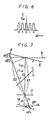
- Fig. 6 shows the cyclical property of the level change of the tracking error signal Se in response to the tangential skew angle ⁇ ° of the 0-order beam L 0 relative to the recording surface of the optical recording medium 6 when one beam Lb of the both side beams Lb and Lc is introduced into the laser beam emission end face lA of the semiconductor laser element 1, while the other beam Lc is introduced into the heat sink 8.
- is increased, the level of the tracking error signal Se is attenuated.
- the both side beams Lb and Lc are all incident on the laser beam emission end face lA, the amplitude of the waveform corresponding to Fig. 6 becomes twice that in Fig. 6 and the phase thereof becomes different from that in Fig. 6.
- a solid line lA designates the laser beam emission end face which is generally skewed relative to a broken line emission end face lA placed at the normal position.
- a solid line optical recoding medium 6 is inclined relative to a broken line optical recording medium 6 that is placed at the normal position.
- the 0-order beam L 0 is vertical to the laser beam emission end face lA placed at the normal position and the recording surface of the optical recording medium 6 placed at the normal position.
- ⁇ is an angle of the +lst-order beam L +1 relative to the 0-order beam L 0 .
- l 1 designates an optical length between the laser beam emission end face lA and the diffraction grating 3 and 1 2 an optical path length between the diffraction grating 3 and the recording surface of the optical recording medium 6.
- ⁇ l 1 and ⁇ l 2 designate optical path differences of the 0-order beam L 0 and +lst-order beam L +1 relative to the optical path lengths l 1 and l 2 , respectively.
- ⁇ l 3 and ⁇ l 4 respectively designate optical path differences brought about by the skew of the optical recording medium 6 and by the skew of the laser beam emission end face 1A.
- g designates a phase difference between the 0-order beam L 0 and +lst-order beam L +1 in the diffraction grating 3.
- i 0 and i 1 designate transmissivities of the 0-order beam L 0 and +lst-order beam L +1 in the diffraction grating 3, respectively, t a transmissivity of the half mirror 4, and r and f reflectivities on the recording surface of the optical recording medium 6 and on the laser beam emission end face lA, respectively.
- a 1 to a 4 are expressed by the following equations.
- intensity I A of light at the point A is expressed by the following equation.
- the light intensity I A at the point A is expressed exactly the same as that in the Eg. (5), while the light intensity I B at the point B is expressed by the following equation.
- the present invention is to propose the above mentioned optical tracking error detecting apparatus which can produce a tracking error signal that is not changed at all by the change of the tangential skew angle of the 0-order beam of the optical head relative to the optical recording medium.
- An optical head tracking error detecting apparatus of this invention comprising a semiconductor laser element, a diffraction grating to which laser beam from the semiconductor laser element is introduced, a beam splitter through which a 0-order beam and ⁇ lst-order beams emitted from the diffraction grating are passed, an objective lens for converging the C-order beam and the ⁇ lst-order beams from the beam splitter so as to introduce the same on an optical recording medium and a photodetector to which a 0-order beam and flst-order beams reflected on the optical recording medium, passed through the objective lens and then reflected on a reflection surface of the beam splitter are introduced wherein a pair of photo-detection outputs corresponding to the ⁇ lst-order beams are obtained from the photodetector and on the basis of the difference between the pair of photo-detection outputs, there is generated a tracking error signal corresponding to the tracking state of the 0-order beam on the optical recording medium,
- Figs. lA and 1B and Fig. 2 are locational representations showing an embodiment of a main part of an optical head tracking error detecting apparatus according to the present invention and a waveform diagram useful for the explanation thereof
- Fig. 3 is a schematic locational diagram showing a prior art optical head tracking error detecting apparatus
- Figs. 4 and 5 are front views showing one example of a semiconductor laser element used in the conventional optical head tracking error detecting apparatus
- Fig. 6 is a waveform diagram and
- Fig. 7 is a diagram useful for explaining the interference.
- the lenses 9 and 10 such one is desirable which has less aberration, a large effective aperture and a long focal length.
- the focal length is 17mm and NA is 0.14.
- a central aperture lla of the light shielding plate 11 is 60 t m in diameter (or width) and 10 ⁇ m in thickness.
- the wavelength of the laser beam L is 830nm. Further, the spacing between the beams is 75 ⁇ m and the beam spot size on the recording medium 6 is 7 ⁇ m.
- the diverging laser beam emitted from the semiconductor laser element 1 is collimated by the collimator lens 2 as the parallel beam and introduced into the lens 9 by which it is converged.
- the converged beam is further introduced into the lens 10 by which it is collimated again as the parallel beam and then introduced into the diffraction grating 3.
- the light shielding plate 11 is located near the converging point of the converged beam that is passed through the lens 9.
- Reference numeral lla designates the central aperture (slit) of the light shielding plate 11 which is used to pass therethrough only the central beam. Other arrangements are made similar to those in Figs. 3 to 7.
- the central beam La and both the side beams Lb and Lc thereof which are all reflected on the recording medium 6, passed through the objective lens 5, the beam splitter 4 and the diffraction grating 3 and directed to the semiconductor laser element 1 the central beam La passes through the central aperture (slit) lla of the light shileding plate 11, but both side beams Lb and Lc are shielded by the shielding plate 11.
- the light shielding plate 11 is given a light absorbence property or light diffused reflection property on its surface facing to the diffraction grating 3 side.
- curves a and b indicate respectively the level changing characteristics of the tracking error signal Se relative to the tangential skew angle ⁇ ° corresponding to that in Fig. 6 under the state that the lenses 9 and 10 and the light shielding plate 11 are not provided and under the state that they are provided.
- the curve b (broken line) becomes considerably small as compared with the curve a (solid line) in the amplitude level.
- the optical head tracking error detecting apparatus as set forth above, even when the beans reflected or the optical recording medium 6 are directed through the objective lens 5, the beam splitter 4 and the diffraction grating 3 to the semiconductor laser element 1, there is no fear that such beams will be reflected on the laser beam emission end face lA thereof. Therefore, it is possible to obtain the tracking error signal which is not changed at all by the change of the tangential skew angle of the 0-order beam of the optical head OH relative to the optical recording medium 6.
Landscapes
- Physics & Mathematics (AREA)
- Optics & Photonics (AREA)
- Optical Recording Or Reproduction (AREA)
- Optical Head (AREA)
Priority Applications (1)
| Application Number | Priority Date | Filing Date | Title |
|---|---|---|---|
| AT85903393T ATE41258T1 (de) | 1984-07-13 | 1985-07-11 | Vorrichtung zum nachweis eines spurfehlers eines optischen kopfes. |
Applications Claiming Priority (2)
| Application Number | Priority Date | Filing Date | Title |
|---|---|---|---|
| JP14576884A JPS6124033A (ja) | 1984-07-13 | 1984-07-13 | 光学式ヘツドのトラツキング誤差検出装置 |
| JP145768/84 | 1984-07-13 |
Publications (3)
| Publication Number | Publication Date |
|---|---|
| EP0188624A1 true EP0188624A1 (de) | 1986-07-30 |
| EP0188624A4 EP0188624A4 (de) | 1986-12-01 |
| EP0188624B1 EP0188624B1 (de) | 1989-03-08 |
Family
ID=15392710
Family Applications (1)
| Application Number | Title | Priority Date | Filing Date |
|---|---|---|---|
| EP85903393A Expired EP0188624B1 (de) | 1984-07-13 | 1985-07-11 | Vorrichtung zum nachweis eines spurfehlers eines optischen kopfes |
Country Status (6)
| Country | Link |
|---|---|
| US (1) | US4766585A (de) |
| EP (1) | EP0188624B1 (de) |
| JP (1) | JPS6124033A (de) |
| KR (1) | KR930007175B1 (de) |
| DE (1) | DE3568661D1 (de) |
| WO (1) | WO1986000742A1 (de) |
Cited By (3)
| Publication number | Priority date | Publication date | Assignee | Title |
|---|---|---|---|---|
| EP0372629A3 (en) * | 1988-12-05 | 1990-10-17 | N.V. Philips' Gloeilampenfabrieken | Apparatus for optically scanning an information plane |
| EP0351953A3 (de) * | 1988-06-20 | 1992-09-30 | Mitsubishi Denki Kabushiki Kaisha | Optischer Kopf mit Kippkorrekturservomechanismus |
| US5391865A (en) * | 1987-08-24 | 1995-02-21 | Sharp Kabushiki Kaisha | Optical pickup apparatus and optical grating assembly therefor |
Families Citing this family (6)
| Publication number | Priority date | Publication date | Assignee | Title |
|---|---|---|---|---|
| GB2209089B (en) * | 1987-08-26 | 1991-07-03 | Sony Corp | Optical recording and/or reproducing apparatus. |
| DE68924303T2 (de) * | 1988-06-14 | 1996-02-29 | Nippon Electric Co | Optische Kopfanordnung. |
| JPH0778904B2 (ja) * | 1989-01-27 | 1995-08-23 | シャープ株式会社 | 光ピックアップ装置 |
| US5247510A (en) * | 1990-06-29 | 1993-09-21 | Digital Equipment Corporation | Increasing storage density of optical data media by detecting a selected portion of a light spot image corresponding to a single domain |
| JP2973637B2 (ja) * | 1991-09-27 | 1999-11-08 | 松下電器産業株式会社 | 三次元測定装置 |
| CN1253871C (zh) * | 2001-06-29 | 2006-04-26 | 松下电器产业株式会社 | 光盘原盘曝光装置和光盘原盘曝光方法以及针孔机构 |
Family Cites Families (9)
| Publication number | Priority date | Publication date | Assignee | Title |
|---|---|---|---|---|
| US4160269A (en) * | 1971-03-04 | 1979-07-03 | U.S. Philips Corporation | Apparatus for optically reading a phase-modulated optical record carrier |
| NL7506495A (nl) * | 1975-06-02 | 1976-12-06 | Philips Nv | Inrichting voor het uitlezen van een registratie- drager. |
| US4180822A (en) * | 1978-04-13 | 1979-12-25 | Rca Corporation | Optical scanner and recorder |
| JPS56116004A (en) * | 1980-02-20 | 1981-09-11 | Olympus Optical Co Ltd | Lens for video disk |
| US4349901A (en) * | 1980-06-20 | 1982-09-14 | Eastman Kodak Company | Apparatus and method for reading optical discs |
| JPS5814332A (ja) * | 1981-07-16 | 1983-01-27 | Mitsubishi Electric Corp | 光学式情報再生装置 |
| NL8104946A (nl) * | 1981-11-02 | 1983-06-01 | Philips Nv | Inrichting voor het uitlezen en/of inschrijven van een optisch uitleesbare informatiestructuur op een registratiedrager. |
| US4462095A (en) * | 1982-03-19 | 1984-07-24 | Magnetic Peripherals Inc. | Moving diffraction grating for an information track centering system for optical recording |
| JPS5958637A (ja) * | 1982-09-28 | 1984-04-04 | Sony Corp | 光学式再生装置 |
-
1984
- 1984-07-13 JP JP14576884A patent/JPS6124033A/ja active Granted
-
1985
- 1985-07-11 EP EP85903393A patent/EP0188624B1/de not_active Expired
- 1985-07-11 KR KR1019860700143A patent/KR930007175B1/ko not_active Expired - Fee Related
- 1985-07-11 DE DE8585903393T patent/DE3568661D1/de not_active Expired
- 1985-07-11 US US06/844,178 patent/US4766585A/en not_active Expired - Lifetime
- 1985-07-11 WO PCT/JP1985/000391 patent/WO1986000742A1/ja not_active Ceased
Cited By (4)
| Publication number | Priority date | Publication date | Assignee | Title |
|---|---|---|---|---|
| US5391865A (en) * | 1987-08-24 | 1995-02-21 | Sharp Kabushiki Kaisha | Optical pickup apparatus and optical grating assembly therefor |
| EP0351953A3 (de) * | 1988-06-20 | 1992-09-30 | Mitsubishi Denki Kabushiki Kaisha | Optischer Kopf mit Kippkorrekturservomechanismus |
| US5216649A (en) * | 1988-06-20 | 1993-06-01 | Mitsubishi Denki Kabushiki Kaisha | Optical head with a tilt correction servo mechanism |
| EP0372629A3 (en) * | 1988-12-05 | 1990-10-17 | N.V. Philips' Gloeilampenfabrieken | Apparatus for optically scanning an information plane |
Also Published As
| Publication number | Publication date |
|---|---|
| EP0188624A4 (de) | 1986-12-01 |
| JPH0513334B2 (de) | 1993-02-22 |
| US4766585A (en) | 1988-08-23 |
| DE3568661D1 (en) | 1989-04-13 |
| WO1986000742A1 (fr) | 1986-01-30 |
| EP0188624B1 (de) | 1989-03-08 |
| JPS6124033A (ja) | 1986-02-01 |
| KR930007175B1 (ko) | 1993-07-31 |
Similar Documents
| Publication | Publication Date | Title |
|---|---|---|
| EP0219908B1 (de) | Gerät zur optischen Abtastung einer Informationsebene | |
| US5016954A (en) | Optical pickup and hologram therefor | |
| KR920010949B1 (ko) | 광전자식 포커싱 오차 검출 시스템 | |
| US4987292A (en) | Method and apparatus for detecting focus and tracking errors | |
| EP0188624A1 (de) | Vorrichtung zum nachweis eines spurfehlers eines optischen kopfes | |
| US4742506A (en) | Tracking error detecting apparatus for an optical head with skew error reduction by using an inclined header portion | |
| EP0612064B1 (de) | Optische Abtastvorrichtung | |
| US5231621A (en) | Focus detector which serves to split off a portion of a detected light beam only when the detected light beam is not refocused at an expected refocus point | |
| US5745304A (en) | Integrated optical pickup system capable of reading optical disks of different thickness | |
| JP3762440B2 (ja) | 光学式走査装置 | |
| US5570334A (en) | Optical pickup with a double refraction polarizing plate to split light beams into two polarized beams | |
| KR940004656B1 (ko) | 광학식 헤드의 트랙킹 오차 검출장치 | |
| KR930002163B1 (ko) | 광학식 헤드의 트랙킹 오차 검출장치 | |
| JPH09259457A (ja) | 光エミッタ−レシーバ装置及び光学読み取りシステム | |
| EP0605929B1 (de) | Vorrichtung zur optischen Abtastung einer Fläche | |
| JP2575099B2 (ja) | 光学式ヘツドのトラツキング誤差検出装置 | |
| EP0543481B1 (de) | Optisches Informationsaufnahmegerät mit abgetrennt-eingeordneten Fotodetektoreinrichtungen | |
| KR930007176B1 (ko) | 광학식 헤드의 트랙킹 오차 검출 장치 | |
| KR930002162B1 (ko) | 광학식 헤드의 트랙킹 오차 검출장치 | |
| JP3108976B2 (ja) | 光ヘッドのトラッキング誤差検出装置 | |
| KR0137246B1 (ko) | 콤팩트 디스크 플레이어의 광 픽업장치 (optical pick-up device of compact disc player) | |
| JPH0573918A (ja) | 光学式再生装置 | |
| JPS6265247A (ja) | 光学式ピツクアツプ装置 | |
| JPH058501B2 (de) | ||
| KR20000012240U (ko) | 회절미러를 갖는 홀로그램 소자 |
Legal Events
| Date | Code | Title | Description |
|---|---|---|---|
| PUAI | Public reference made under article 153(3) epc to a published international application that has entered the european phase |
Free format text: ORIGINAL CODE: 0009012 |
|
| 17P | Request for examination filed |
Effective date: 19860325 |
|
| AK | Designated contracting states |
Kind code of ref document: A1 Designated state(s): AT DE FR GB IT NL |
|
| A4 | Supplementary search report drawn up and despatched |
Effective date: 19861201 |
|
| 17Q | First examination report despatched |
Effective date: 19880510 |
|
| GRAA | (expected) grant |
Free format text: ORIGINAL CODE: 0009210 |
|
| AK | Designated contracting states |
Kind code of ref document: B1 Designated state(s): AT DE FR GB IT NL |
|
| REF | Corresponds to: |
Ref document number: 41258 Country of ref document: AT Date of ref document: 19890315 Kind code of ref document: T |
|
| REF | Corresponds to: |
Ref document number: 3568661 Country of ref document: DE Date of ref document: 19890413 |
|
| ET | Fr: translation filed | ||
| ITF | It: translation for a ep patent filed | ||
| PLBE | No opposition filed within time limit |
Free format text: ORIGINAL CODE: 0009261 |
|
| STAA | Information on the status of an ep patent application or granted ep patent |
Free format text: STATUS: NO OPPOSITION FILED WITHIN TIME LIMIT |
|
| 26N | No opposition filed | ||
| ITTA | It: last paid annual fee | ||
| REG | Reference to a national code |
Ref country code: GB Ref legal event code: IF02 |
|
| PGFP | Annual fee paid to national office [announced via postgrant information from national office to epo] |
Ref country code: GB Payment date: 20030709 Year of fee payment: 19 |
|
| PGFP | Annual fee paid to national office [announced via postgrant information from national office to epo] |
Ref country code: FR Payment date: 20030711 Year of fee payment: 19 Ref country code: AT Payment date: 20030711 Year of fee payment: 19 |
|
| PGFP | Annual fee paid to national office [announced via postgrant information from national office to epo] |
Ref country code: DE Payment date: 20030724 Year of fee payment: 19 |
|
| PGFP | Annual fee paid to national office [announced via postgrant information from national office to epo] |
Ref country code: NL Payment date: 20030730 Year of fee payment: 19 |
|
| PG25 | Lapsed in a contracting state [announced via postgrant information from national office to epo] |
Ref country code: GB Free format text: LAPSE BECAUSE OF NON-PAYMENT OF DUE FEES Effective date: 20040711 Ref country code: AT Free format text: LAPSE BECAUSE OF NON-PAYMENT OF DUE FEES Effective date: 20040711 |
|
| PG25 | Lapsed in a contracting state [announced via postgrant information from national office to epo] |
Ref country code: NL Free format text: LAPSE BECAUSE OF NON-PAYMENT OF DUE FEES Effective date: 20050201 Ref country code: DE Free format text: LAPSE BECAUSE OF NON-PAYMENT OF DUE FEES Effective date: 20050201 |
|
| GBPC | Gb: european patent ceased through non-payment of renewal fee |
Effective date: 20040711 |
|
| PG25 | Lapsed in a contracting state [announced via postgrant information from national office to epo] |
Ref country code: FR Free format text: LAPSE BECAUSE OF NON-PAYMENT OF DUE FEES Effective date: 20050331 |
|
| NLV4 | Nl: lapsed or anulled due to non-payment of the annual fee |
Effective date: 20050201 |
|
| REG | Reference to a national code |
Ref country code: FR Ref legal event code: ST |