EP0189523B1 - Mikroprozessorsystem - Google Patents
Mikroprozessorsystem Download PDFInfo
- Publication number
- EP0189523B1 EP0189523B1 EP85112374A EP85112374A EP0189523B1 EP 0189523 B1 EP0189523 B1 EP 0189523B1 EP 85112374 A EP85112374 A EP 85112374A EP 85112374 A EP85112374 A EP 85112374A EP 0189523 B1 EP0189523 B1 EP 0189523B1
- Authority
- EP
- European Patent Office
- Prior art keywords
- address
- memory
- microprocessor
- instruction
- data
- Prior art date
- Legal status (The legal status is an assumption and is not a legal conclusion. Google has not performed a legal analysis and makes no representation as to the accuracy of the status listed.)
- Expired - Lifetime
Links
Images



Classifications
-
- G—PHYSICS
- G06—COMPUTING OR CALCULATING; COUNTING
- G06F—ELECTRIC DIGITAL DATA PROCESSING
- G06F13/00—Interconnection of, or transfer of information or other signals between, memories, input/output devices or central processing units
-
- G—PHYSICS
- G11—INFORMATION STORAGE
- G11C—STATIC STORES
- G11C11/00—Digital stores characterised by the use of particular electric or magnetic storage elements; Storage elements therefor
- G11C11/21—Digital stores characterised by the use of particular electric or magnetic storage elements; Storage elements therefor using electric elements
- G11C11/34—Digital stores characterised by the use of particular electric or magnetic storage elements; Storage elements therefor using electric elements using semiconductor devices
- G11C11/40—Digital stores characterised by the use of particular electric or magnetic storage elements; Storage elements therefor using electric elements using semiconductor devices using transistors
- G11C11/41—Digital stores characterised by the use of particular electric or magnetic storage elements; Storage elements therefor using electric elements using semiconductor devices using transistors forming static cells with positive feedback, i.e. cells not needing refreshing or charge regeneration, e.g. bistable multivibrator or Schmitt trigger
- G11C11/413—Auxiliary circuits, e.g. for addressing, decoding, driving, writing, sensing, timing or power reduction
- G11C11/417—Auxiliary circuits, e.g. for addressing, decoding, driving, writing, sensing, timing or power reduction for memory cells of the field-effect type
- G11C11/419—Read-write [R-W] circuits
-
- G—PHYSICS
- G06—COMPUTING OR CALCULATING; COUNTING
- G06F—ELECTRIC DIGITAL DATA PROCESSING
- G06F13/00—Interconnection of, or transfer of information or other signals between, memories, input/output devices or central processing units
- G06F13/38—Information transfer, e.g. on bus
- G06F13/40—Bus structure
- G06F13/4004—Coupling between buses
- G06F13/4009—Coupling between buses with data restructuring
- G06F13/4018—Coupling between buses with data restructuring with data-width conversion
-
- G—PHYSICS
- G06—COMPUTING OR CALCULATING; COUNTING
- G06F—ELECTRIC DIGITAL DATA PROCESSING
- G06F15/00—Digital computers in general; Data processing equipment in general
Definitions
- the present invention relates to a microprocessor system configured by connecting a memory and/or I/O having an n/2-bit data bus width to a microprocessor having an n-bit data bus width.
- a programmer must create a program by considering combinations of the architecture of the system and executable instructions (1-/2-/4-byte access instructions or the like). Since a word transfer instruction cannot be used in the 8-bit peripheral control LSI, existing software for 16-bit microprocessors must be rewritten such that a 16-bit word instruction is replaced with two byte transfer instructions.
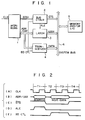
- Fig. 1 is a block diagram of a conventional microprocessor system.
- the system comprises a microprocessor ( ⁇ CPU 8086) 1, a bus controller (BUS CTRLR) 2, a latch (LATCH) 3, a bus transceiver (TRANSCEIVER) 4, a memory and/or I/O (MEMORY AND/OR I/O) (to be referred to as a memory hereinafter) 5 having a 16-bit data bus width, and a system bus 6.
- the microprocessor 1 comprises, for example, a microprocessor 8086 available from Intel Corp., U.S.A.
- the microprocessor 1 receives a clock CLK and sends status data STS1 to the controller 2.
- the controller 2 Upon reception of the data STS1, the controller 2 supplies a read/write control signal STS to the memory 5 or the like.
- the microprocessor 1 is connected to the latch 3 and the transceiver 4 through an address data bus ADR/DAT.
- the microprocessor 1 supplies an address signal to the latch 3 and a data signal to the transceiver 4.
- the latch 3 receives the address signal from the microprocessor and supplies an address ADDR to the memory 5.
- the transceiver 4 is connected to the memory 5 through a data bus DATA and the bus 6, and transfers data from or to the memory 5.
- the controller 2 supplies a signal ALE to the latch 3 and a signal BDCTL to the transceiver 4.
- the signal ALE controls a latch timing of the address, and the signal BDCTL controls the input/output of the transceiver 4.
- Figs. 2A to 2E are timing charts explaining a read cycle word transfer instruction starting from an even address in the circuit of Fig. 1.
- the machine cycle basically consists of clocks (CLK) T1, T2, T3 and T4, as shown in Fig. 2A.
- the microprocessor 1 In the read cycle starting from the even address, the microprocessor 1 generates the address and the status data in response to the clock T1, as shown in Fig. 2B.
- the controller 2 supplies the signal ALE to the latch 3 in response to the status data, as shown in Fig. 2D.
- the controller 2 supplies the signal STS to the memory 5, as shown in Fig. 2C.
- the latch 3 latches the address in response to the signal ALE generated from the controller 2.
- 16-bit data is read out from the memory 5 onto the bus DATA, and the transceiver 4 sends the 16-bit data shown in Fig. 2B from the memory 5 onto the bus ADR/DAT by the control signal BDCTL shown in Fig. 2E from the bus controller 2.
- the microprocessor 1 fetches the data at the trailing edge of the clock T3.
- the word transfer instruction of the read cycle starting from an odd address there are two access cycles. Data fetching is performed in the same manner as in the read cycle starting from an even address. However, in the first access cycle, the data corresponding to the start even address is fetched as the most significant part of the 16-bit data. The address is then updated, and in the second access cycle, the data corresponding to the start odd address is fetched as the least significant part. In this manner, 16-bit data is thus fetched by the microprocessor 1.
- the above operation can be performed in the same manner as in the word transfer instruction of the write cycle.
- the prior art microprocessor system has a 16-byte boundary. Although one address has 1-byte data, the address has, as its objective, a memory of basically a 16-bit data bus width. For this reason, the microprocessor system configuration is not flexible, resulting in inconvenience (see MEMORY ORGANIZATION of MICROPROCESSOR AND PERIPHERALS HANDBOOK 1983 published by Intel Corp. for further reference).
- This method comprises the steps of: (a) extracting a read/write control signal for said memory and/or I/O from status data generated from said microprocessor when said microprocessor executes the word transfer instruction, supplying the read/write control signal together with an address to said memory and/or I/O setting a bus converter for connecting a data bus coupled to said memory and/or I/O with a n-bit data bus width, and starting a first access cycle, and (b) causing said microprocessor to inhibit generation of the read/write control signal to complete the word transfer instruction.
- a first access cycle for said memory and/or I/O is performed said first step comprising: a step of detecting that the instruction executed by said microprocessor is a word transfer instruction for said memory and/or I/O; a step of setting said microprocessor in a wait state before the first access cycle is completed and when the instruction is determined to be the word transfer instruction for said memory and/or I/O; and a step of inhibiting generation of the read/write control signal to complete the first access cycle.
- the address is updated by adding 1 to the address while the read/write control signal is disabled and the updated address is supplied to said memory and/or I/O and the read/write control signal is enabled again to start the second access cycle.
- a second access cycle for said memory and/or I/O is performed the wait state of said microprocessor being cancelled during said second access cycle.
- the present invention provides a microprocessor system and a method as defined in claims 1 and 11, respectively.
- a software programmer need not selectively use the word transfer instruction and the byte transfer instruction in accordance with the data bus width of the memory and/or I/O. In other words, the programmer can always use word transfer instructions.
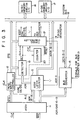
- Fig. 3 is a block diagram of a microprocessor system configured by connecting a memory and/or I/O 17 having an 8-bit data bus width to a 16-bit microprocessor 11.
- the microprocessor system comprises the microprocessor 11, a read/write controller 12, an address latch counter 13, a timing generator 14, a bus converter 15, a 16-bit memory and/or I/O 16, the 8-bit memory and/or I/O 17, and a system bus 18.
- the timing generator 14 further comprises a detector 19, a counter 20, and a timing controller 21.
- the microprocessor 11 receives a clock CLK and a wait control signal WAIT from the controller 21 and supplies status data STS1 to the controller 12 and an address ADR 19-0 to the counter 13.
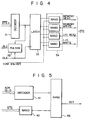
- the controller 12 comprises a decoder 31, a pulser 32, a latch 33 and a gate 34, as shown in Fig. 4.
- the decoder 31 decodes the status data STS1 supplied from the microprocessor 11 and supplies the decoded data to the pulser 32 and the latch 33.
- the pulser 32 supplies an address latch enable signal ALE to the counter 13 in response to the clock CLK.
- the latch 33 latches the outputs from the decoder 31 in response to the clock CLK, and the latched data is supplied to the gate 34.
- the gate 34 supplies, to the detector 19 and the controller 21, a read/write control signal STS representing the memory or I/O write or read mode, and controlled by the control signal COM EN/ DIS from the controller 21 to be described later.
- the gate 34 also supplies the read/write control signal STS to the memories and/or I/Os 16 and 17 through the bus 18.
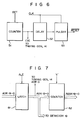
- the address latch counter 13 comprises a latch 61 and a counter 62, as shown in Fig. 7.
- the latch 61 latches the address ADR 19-0 from the microprocessor 11 in response-to the signal ALE from the controller 12.
- An address ADR 19-0 is supplied to the counter 62 and the detector 19.
- the least significant bit ADR 0 of the address is supplied to the controller 21.
- the counter 62 receives, as a preset value, the output from the latch 61, and is counted up in response to a signal of logic "1" from the controller 21.
- the updated address data is supplied from the counter 62 to the memories and/or I/Os 16 and 17 through a bus ADDR 19-0 and the bus 18.
- the detector 19 comprises a decoder 41 and gates 42 and 43, as shown in Fig. 5.
- the decoder 41 decodes the address data ADR 19-0 generated from the counter 13 and supplies the decoded result to the gate 43.
- the gate 42 calculates the NAND product of the read/write control signals STS as outputs from the controller 12 and supplies the NAND signal to the gate 43.
- the gate 43 also calculates the NAND product of the inputs.
- the gate 43 supplies a detection signal DET to the counter 20 and the controller 21.
- the counter 20 comprises a counter 51, a delay 52 and a pulser 53, as shown in Fig. 6.
- the counter 51 counts the output signal DET from the detector 19.
- the counter 51 supplies a signal CYC to the controller 21 and the delay 52.
- the delay 52 receives the output from the counter 51 and the clock signal CLK.
- the delay 52 supplies a signal to the pulser 53.
- the pulser 53 supplies a signal RESET to the controller 21 to reset the controller 21.
- the microprocessor 11 exchanges data with the converter 15 through a data bus DAT.
- the converter 15 comprises bidirectional bus drivers 71, 73 and 75, and latches 72 and 74.
- a set of the driver 71 and the latch 72, and another set of the driver 73 and the latch 74 are connected in parallel between the data buses DAT 15-8 and DATA 15-8, and between the data buses DAT 7-0 and DATA 7-0.
- the latches 72 and 74 are connected to supply data to the microprocessor 11.
- the driver 75 is arranged to connect the bus DATA 15-8 to the bus DATA 7-0.
- the converter 15 receives from the controller 21 control signals BD1EN and BD1DIR for the driver 71, control signals BD2EN and BD2DIR for the driver 73, control signals BD3EN and BD3DIR for the driver 75, control signals LT2CNT and LT2EN for the latch 72, and control signals LT1CNT and LT1EN for the latch 74.
- the memories and/or I/Os 16 and 17 receive the signal STS and an address ADDR.
- a data bus DATA 15-0 is connected to the 16-bit memory and/or I/O 16
- the bus DATA 7-0 is connected to the 8-bit memory and/or I/O 17.
- the memory and/or I/O 17 is connected to a previously assigned address.
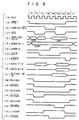
- the operation of the microprocessor system of this embodiment will be described with reference to the timing charts of Figs. 9A to 11T.
- the clock signal CLK basically consists of clock pulses T1, T2, T3 and T4.
- TW When the microprocessor 11 is held in the wait state, the clock signal CLK is represented by TW.
- the microprocessor 11 executes the word transfer instruction, it supplies the status STS1 to the controller 12, as shown in Fig. 9B.
- the microprocessor 11 also supplies the address to the address latch counter 13, as shown in Fig. 9E.
- the counter 13 latches the address in response to a latch control signal ALE from the read/write controller 12, as shown in Figs.
- the signals BD1EN , BD2EN , BD3EN and LT1EN are output enable/disable signals.
- the signals BD1DIR, BD2DIR and BD3DIR are output direction control signals.
- the signal is output from the directions A to B illustrated in Fig. 8.
- the signal is output from direction B to direction A when the signal BD1DIR, BD2DIR or BD3DIR is set at a low level.
- the signal LT1CNT is a latch timing control signal.
- the drivers 71 and 73 are operated to supply data from the memories and/or I/Os 16 and 17 to the microprocessor 11.
- the detector 19 detects, in accordance with the read/write control signal and the address, that the instruction is an instruction for the 8-bit memory and/or I/O 17, the detector 19 supplies the DET signal to the controller 21.
- the controller 21 then supplies the signal WAIT to the microprocessor 11, as shown in Fig. 9H, so as to set the microprocessor 11 in the wait state.
- the data from the memory and/or I/O 17 is sent onto the bus DAT 7-0.
- the microprocessor 11 does not fetch data.
- the controller 21 supplies the signal LT1CNT to the latch 74, so that the data on the bus DAT 7-0 is latched by the latch 74.
- the controller 21 supplies the signal BD2EN to the driver 73 to inhibit data output, as shown in Fig. 9P.
- the controller 21 supplies the signal COM EN/ DIS to the controller 12 to inhibit generation of the signal STS .
- the read/write control signal STS is disabled.
- the controller 21 supplies a signal of logic "1" to the counter 62.
- the counter 62 sends the updated address onto an address bus ADDR. As shown in Fig.
- the controller 21 supplies the signal LT1EN to the latch 74.
- the latch 74 sends the data onto the data bus DAT 7-0, as shown in Fig. 9L.
- the controller 21 supplies the signal COM EN/ DIS to the controller 12 to enable generation of the read/write control signal STS .
- the signal STS is enabled again so that the second access cycle can be started.
- the driver 75 supplies the data read out from the memory and/or I/O 17 to the bus DATA 15-8 through the bus DATA 7-0, as shown in Figs. 9J and 9K, in response to the signal BD3EN (Fig. 9R) from the controller 21.
- Figs. 9R the signal BD3EN
- the driver 71 sends the data from the bus DATA 15-8 onto the bus DAT 15-8 in response to the signal BD1EN from the controller 21.
- the 16-bit data appears on the bus DAT 15-0.
- the controller 21 generates the signal WAIT , as shown in Fig. 9H, so that the wait state of the microprocessor 11 is cancelled.
- the microprocessor 11 fetches the 16-bit data and inhibits generation of the data STS1 , as shown in Fig. 9B.
- the signal STS is also inhibited.
- the pulser 53 supplies the signal RESET to the controller 21, as shown in Fig. 91.
- the controller 21 resets the signals BD1EN , BD3EN , LT1CNT and LT1EN , as shown in Figs. 9N, 9R, 9S and 9T, respectively. Subsequently, the controller 21 resets the signals BD1DIR, BD2DIR and BD3DIR (Figs. 9M, 90 and 9Q). In this manner, conversion operation is completed. In a read cycle starting with an even address, the latch 72 is kept disabled.
- a write cycle starting with an even address will be described with reference to Figs. 10A to 10T.
- the clock signal CLK, the data STS1 , the control signal COM EN/ DIS , the read/write control signal STS , the control signal WAIT for the microprocessor 11, the reset signal RESET and the signal of logic "1" are the same as those of the read cycle starting with the even address.
- the signals associated with the converter 15 will mainly be considered in the following description.
- the drivers 71 and 73 are operated to supply 16-bit data to the memory and/or I/O 16, as shown in Figs. 10M, 10N, 100 and 10P. Since the driver 75 is disabled, as shown in Fig.
- the driver 73 supplies data from the bus DAT 7-0 to the bus DATA 7-0, as shown in Fig. 10J. This data is transferred to the memory and/or I/O 17 through the bus DATA 7-0.
- the driver 71 is kept enabled, as shown in Figs. 10M and 10N. However, the driver 73 is disabled, as shown in Fig. 10P. Instead, the driver 75 is enabled, as shown in Fig. 10R. For this reason, the most significant part of the 16-bit data generated from the microprocessor 11 is supplied by the drivers 71 and 75 to the memory and/or I/O 17 through the bus DATA 7-0, as shown in Fig. 10J.
- the latches 72 and 74 are kept disabled. In this manner, the write cycle with the even address is executed.
- the clock signal CLK, the data STS1, the control signal COM EN/ DIS , the read/write control signal STS , the control signal WAIT for the microprocessor 11, the reset signal RESET and the signal of logic "1" are the same as those of a read cycle starting with an even address.
- the signals associated with the converter 15 will be considered in the following description.
- the drivers 71 and 73 are operated to supply the 16-bit data from the memory and/or I/O 16 to the microprocessor 11, as shown in Figs. 11M, 11N, 110 and 11P.
- the converter 75 is held operative, as shown in Figs.
- the data (Fig. 11J) read out from the memory and/or I/O 17, and appearing on the bus DATA 7-0 is sent onto the bus DATA 15-8, as shown in Fig. 11K.
- the drivers 71 and 73 transfer the data from the bus DATA 15-0 to the bus DAT 15-0, as shown in Fig. 11E.
- the microprocessor 11 is held in the wait state, as shown in Fig. 11H, and does not fetch the data.
- the controller 21 supplies the signal LT2CNT to the latch 72, as shown in Fig. 11S, so that the latch 72 latches the data.
- the controller 21 supplies the signal BD1EN and BD3EN to the drivers 71 and 75, as shown in Figs.
- the latch 72 sends the data onto the bus DAT 15-8, as shown in Fig. 11L.
- the driver 73 sends the data read out from the memory and/or I/O 17 onto the bus DAT 7-0, as shown in Fig. 11K. Therefore, as shown in Fig. 11E, the 16-bit data appears on the bus DAT 15-0.
- the wait state of the microprocessor 11 is cancelled in response to the signal WAIT from the controller 21, as shown in Fig. 11H, and the microprocessor 11 fetches the 16-bit data. In this manner, the read cycle starting with the odd address is completed. In the read cycle starting from the odd address, the latch 74 is kept disabled.
- the output CYC from the counter 20 can be omitted when the controller 21 performs sequential operation.
- a read/write word transfer instruction is performed for the memory and/or I/O 16 having the 16-bit data bus width, the operation is performed at timings as shown in Figs. 2A to 2E.
- the microprocessor 11 comprises a 8086 available from Intel Corp.
- the latch 72 in the converter 15 can be omitted.
- a portion for controlling the latch 72 can also be omitted from the controller 21.
- the address latch counter 13 can be simplified, as shown in Fig. 12.
- the counter 13 comprises a latch 81 and a gate 82.
- the latch 81 latches the address from the microprocessor 11 and supplies the least significant bit thereof to the controller 21 and the gate 82.
- the remaining bits of the address are sent from the latch 81 onto an address bus ADDR 19-1.
- the gate 82 calculates a logical OR of the output from the latch 81 and the logic "1" from the controller 21, and generates the sum as the least significant bit of the address data. All bits of the address signal appear on the address bus ADDR and are supplied to the memories and/or I/Os 16 and 17.
- the timing charts of this microprocessor system are the same as those of the word transfer instruction starting with an even address in Figs. 9A to 10T.
- the present invention is exemplified by a microprocessor system configured by connecting an 8-bit memory and/or I/O to a 16-bit microprocessor.
- a 16-bit memory and/or I/O may be connected to a 32-bit microprocessor, or a 32-bit memory and/or I/O may be connected to a 64-bit microprocessor.
Landscapes
- Engineering & Computer Science (AREA)
- Theoretical Computer Science (AREA)
- General Engineering & Computer Science (AREA)
- Computer Hardware Design (AREA)
- Physics & Mathematics (AREA)
- General Physics & Mathematics (AREA)
- Microelectronics & Electronic Packaging (AREA)
- Bus Control (AREA)
Claims (11)
- Mikroprozessorsystem zur Wandlung einer Übergabeanweisung für ein Wort in eine Übergabeanweisung für 1/2 Wort, welches folgendes umfaßt:
einen Mikroprozessor mit einem n Bit breiten Datenbus (11);
einen Speicher und/oder ein E/A-Gerät mit einem n/2 Bit breiten Datenbus (17);
eine Lese-/Schreibsteuerungseinrichtung (12) zur Lieferung eines aus den Statusdaten des Mikroprozessors (11) abgeleiteten Lese-/Schreibsteuersignals an den Speicher und/oder an das E/A-Gerät (17);
eine Adreßsignalspeicher-Zählereinrichtung (13) zum Holen einer Adresse aus dem Mikroprozessor (11) und zur Lieferung der Adresse an den Speicher und/oder das E/A-Gerät (17);
eine Taktgeneratoreinrichtung (14) zur Generierung von Steuersignalen mit einem Status zum Zugriff auf einen n Bit breiten Speicher oder ein E/A-Gerät (16); und
eine Buswandlereinrichtung (15) zum Setzen eines Busses in einen Status für den Zugriff auf den Speicher oder das E/A-Gerät (16) mit dem n Bit breiten Datenbus als Reaktion auf die Steuersignale;
wobei die Lese-/Schreibsteuerungseinrichtung (12) des weiteren eine Schaltungseinrichtung zur Ausführung der beiden Zugriffszyklen umfaßt, indem das Lese-/Schreibsteuersignal durch ein Steuersignal aktiviert/deaktiviert wird;
wobei die Adreßsignalspeicher-Zählereinrichtung (13) des weiteren eine Schaltungseinrichtung zur Lieferung der zwischengespeicherten Adresse an die Taktgeneratoreinrichtung (14), zur Aktualisierung der Adreßdaten als Reaktion auf das Steuersignal von der Taktgeneratoreinrichtung (14), während das Lese-/Schreibsteuersignal deaktiviert ist, und zur Lieferung einer aktualisierten Adresse an den Speicher und/oder das E/A-Gerät (17) enthält;
wobei die Buswandlereinrichtung (15) des weiteren eine auf die Steuersignale ansprechende und so arbeitende Schaltungseinrichtung enthält, daß das n Bit breite Datum des Mikroprozessors (11) in zwei n/2 Bit breite Daten geteilt wird, und die Daten durch die beiden Zugriffszyklen entsprechend der Adresse, auf die die Einschreibanweisung zugreift, an den Speicher und/oder die E/A-Einheit (17) ausgegeben werden, so daß sie mit dem n/2 Bit breiten Datum aus der Zugriffsadresse in dem Speicher und/oder dem E/A-Gerät (17) durch die Anweisung, ein n Bit breites Datum zu bilden, kombiniert und im Lesezyklus an den Mikroprozessor (11) ausgegeben werden; und
wobei die Taktgeneratoreinrichtung (14) des weiteren eine Schaltungseinrichtung zur Lieferung von Steuersignalen an den Mikroprozessor (11), die Lese-/Schreibsteuerungseinrichtung (12), die Adreßsignalspeicher-Zählereinrichtung (13) und die Buswandlereinrichtung (15), um die Wandlung einer Wortübergabeanweisung in zwei 1/2-Wort-Übergabeanweisungen zu gestatten; und eine Einrichtung zur Erkennung, daß es sich bei der Anweisung um die Wortübergabeanweisung für den Speicher und/oder das E/A-Gerät handelt, enthält;
dadurch gekennzeichnet, daß
die Detektoreinrichtung des weiteren erkennt, ob die Startadresse, auf die die Anweisung zugreift, eine gerad- oder ungeradzahlige Adresse ist;
wobei die Buswandlereinrichtung (15) als Reaktion auf Steuersignale in einem ersten Zugriffszyklus so arbeitet, daß dann, wenn die Anweisung als eine Wortübergabeanweisung eines Lesezyklus erkannt wird und ab der geradzahligen Adresse beginnt, das Datum von dem Speicher und/oder dem E/A-Gerät (17) als der niedrigstwertige Teil des n Bit breiten Datums zwischengespeichert wird, während in dem Fall, in dem die Wortübergabeanweisung des Lesezyklus ab der ungeradzahligen Adresse beginnt, das Datum von dem Speicher und/oder dem E/A-Gerät (17) als der höchstwertige Teil des n Bit breiten Datums zwischengespeichert wird, so daß dann, wenn die Anweisung als eine Wortübergabeanweisung eines Schreibzyklus erkannt wird und ab der geradzahligen Adresse beginnt, der niedrigstwertige Teil des vom Mikroprozessor (11) generierten n Bit breiten Datums an den Speicher und/oder das E/A-Gerät (17) geliefert wird, und in dem Fall, in dem die Wortübergabeanweisung des Schreibzyklus ab der ungeradzahligen Adresse beginnt, der höchstwertige Teil an den Speicher und/oder das E/A-Gerät (17) geliefert wird; und die Buswandlereinrichtung (15) in einem zweiten Zugriffszyklus so arbeitet, daß dann, wenn die Anweisung als Wortübergabeanweisung eines Lesezyklus erkannt wird und ab der geradzahligen Adresse beginnt, das Datum von dem Speicher und/oder dem E/A-Gerät (17) als der höchstwertige Teil des n Bit breiten Datums und zusammen mit dem Datum des ersten Zugriffszyklus an den Mikroprozessor (11) geliefert wird, und in dem Fall, in dem die Wortübergabeanweisung des Lesezyklus ab der ungeradzahligen Adresse beginnt, das Datum von dem Speicher und/oder dem E/A-Gerät (17) als der niedrigstwertige Teil des n Bit breiten Datums und zusammen mit dem Datem des ersten Zugriffszyklus an den Mikroprozessor (11) geliefert wird, so daß dann, wenn die Anweisung als Wortübergabeanweisung des Schreibzyklus erkannt wird und ab der geradzahligen Adresse beginnt, der höchstwertige Teil des n Bit breiten Datums von dem Mikroprozessor (11) an den Speicher und/oder das E/A-Gerät (17) geliefert wird, und in dem Fall, in dem die Wortübergabeanweisung des Schreibzyklus ab der ungeradzahligen Adresse beginnt, der niedrigstwertige Teil des n Bit breiten Datums an den Speicher und/oder das E/A-Gerät (17) geliefert wird. - Mikroprozessorsystem gemäß Anspruch 1, dadurch gekennzeichnet, daß die Lese-/Schreibsteuerungseinrichtung (12) des weiteren eine Schaltungseinrichtung zur Lieferung eines Steuersignals zur Zwischenspeicherung einer Adresse des Mikroprozessors (1) in der Adreßsignal-Zählereinrichtung (13) umfaßt.
- Mikroprozessorsystem gemäß Anspruch 2, dadurch gekennzeichnet, daß die Lese-/Schreibsteuerungseinrichtung (12) einen Decodierer, einen Signalspeicher, eine Gateschaltung und einen Impulsgeber umfaßt, wobei der Decodierer zur Decodierung der vom Mikroprozessor (11) generierten Statusdaten arbeitet, der Impulsgeber als Reaktion auf einen Ausgang des Decodierers ein Zwischenspeicherungstaktsteuersignal an die Adreßsignalspeicher-Zählereinrichtung (13) liefert, der Signalspeicher den Ausgang des Decodierers zwischenspeichert, die Gateschaltung zur Steuerung der Generierung des Lese-/Schreibsteuersignals durch eine logische Operation eines Ausgangs des Signalspeichers und eine Ausgangs der Taktgeneratoreinrichtung (14) arbeitet, und ein Ausgang der Gateschaltung an die Taktgeneratoreinrichtung (14) und den Speicher und/oder das E/A-Gerät (17) geliefert wird.
- Mikroprozessorsystem gemäß Anspruch 1, dadurch gekennzeichnet, daß die Adreßsignalspeicher-Zählereinrichtung (13) eine Signalspeicher- und eine Zählerschaltung umfaßt, wobei der Signalspeicher als Reaktion auf das Steuersignal von der Lese-/Schreibsteuerungseinrichtung (12) aktiviert wird, um die Adresse von dem Mikroprozessor zwischenzuspeichern und um die Adresse als einen voreingestellten Wert an die Zählerschaltung und an den Taktgenerator zu liefern, um zu erkennen, daß die Anweisung eine Wortübergabeanweisung für den Speicher und/oder das E/A-Gerät (17) ist und dann, ob die Startadresse, auf welche die Anweisung zugreift, eine gerad- oder ungeradzahlige Adresse ist, und wobei die Zählerschaltung aktiviert wird, um die Adresse aus dem Signalspeicher als einen voreingestellten Wert an den Speicher und/oder das E/A-Gerät (17) zu liefern, die Adresse als Reaktion auf das Signal von der Taktgeneratoreinrichtung (14) zu inkrementieren, während das Lese-/Schreibsteuersignal deaktiviert ist, und um eine aktualisierte Adresse an den Speicher und/oder das E/A-Gerät (17) zu liefern.
- Mikroprozessorsystem gemäß Anspruch 1, dadurch gekennzeichnet, daß die Adreßsignalspeicher-Zählereinrichtung (13) einen Signalspeicher und ein OR-Gate umfaßt, wenn das System durch Kopplung des Speichers und/oder des E/A-Geräts (17) mit einem 8 Bit breitem Datenbus an einen 16-Bit-Mikroprozessor (11) konfiguriert ist, in welchem nur die mit der geradzahligen Adresse beginnende Wortübergabeanweisung in zwei Byte-übergabeanweisungen zu wandeln ist, wobei der Signalspeicher aktiviert wird, um das vom Mikroprozessor (11) generierte Adreßdatum zwischenzuspeichern und das Adreßdatum an die Taktgeneratoreinrichtung (14) zu liefern, und wobei das OR-Gate aktiviert wird, um eine logische Summe aus dem niedrigstwertigen Bit vom Signalspeicher und einem Adressenaktualisierungssignal von der Taktgeneratoreinrichtung (14) zu bilden, und um das resultierende Signal als Adreßdatum zusammen mit den restlichen Bits der Adresse an den Speicher und/oder das E/A-Gerät (17) zu liefern.
- Mikroprozessorsystem gemäß Anspruch 1, dadurch gekennzeichnet, daß die Buswandlereinrichtung (15) den Datenbus in den höchst- und den niedrigstwertigen Teil teilt und bidirektionale Bustreiber koppelt, um die höchst- oder niedrigstwertigen Teile der mit dem Mikroprozessor (11) und einem n-Bit-Speicher und/oder E/A-Gerät (16) gekoppelten Datenbusse zu verbinden, wobei die bidirektionalen Bustreiber parallel zu Signalspeichern zur Lieferung der Daten aus dem Speicher und/oder dem E/A-Gerät (17) an den Mikroprozessor (11) geschaltet sind und zusätzliche Bustreiber so geschaltet sind, daß sie die höchst- und niedrigstwertigen Teile der mit dem n-Bit-Speicher und/oder dem E/A-Gerät (16) verbundenen Datenbusse koppeln.
- Mikroprozessorsystem gemäß Anspruch 1, dadurch gekennzeichnet, daß dann, wenn der Speicher und/oder das E/A-Gerät (17) mit einem 8 Bit breitem Datenbus mit einem 16-Bit-Mikroprozessor gekoppelt und nur die mit der geradzahligen Adresse beginnende Wortübergabeanweisung in zwei Byte-Übergabeanweisungen zu wandeln ist, die Buswandlereinrichtung (15) den Datenbus in den höchst- und den niedrigstwertigen Teil teilt und bidirektionale Bustreiber koppelt, um die höchst- oder niedrigstwertigen Teile der mit dem Mikroprozessor (11) und dem n-Bit-Speicher und/oder dem E/A-Gerät (16) gekoppelten Datenbusse zu verbinden.
- Mikroprozessorsystem gemäß Anspruch 1, dadurch gekennzeichnet, daß die Taktgeneratoreinrichtung (14) folgendes umfaßt:
eine Detektoreinrichtung (19) zur Bestimmung, daß die Anweisung die Wortübergabeanweisung für den Speicher und/oder das E/A-Gerät ist und zwei Zugriffszyklen erfordert;
eine Wartesteuerungseinrichtung (11) zur Generierung des den Mikroprozessor während des ersten Zugriffszyklus in den Wartezustand versetzenden Steuersignals und zur Aufhebung des Wartezustands des Mikroprozessors während des zweiten Zugriffszyklus, wenn bestimmt wird, daß es sich bei der Anweisung um die Wortübergabeanweisung für den Speicher und/oder das E/A-Gerät (17) handelt;
eine Zählereinrichtung (20) zur Zählung der Anzahl von Malen, in denen die Generierung des Lese-/Schreibsteuersignals gestattet ist, und zum Rücksetzen einer internen Schaltung, wenn der zweite Zugriffszyklus abgeschlossen ist; und
eine Taktgebersteuerungseinrichtung (21) zur Lieferung des Signals zur Steuerung der Generierung des Lese-/Schreibsteuersignals an die Lese-/Schreibsteuerungseinrichtung (12), des Adreßaktualisierungssignals an die Adreßsignalspeicher-Zählereinrichtung (13) und der Signale zur Steuerung der Wandlung an die Buswandlereinrichtung (15). - Mikroprozessorsystem gemäß Anspruch 8, dadurch gekennzeichnet, daß die Detektoreinrichtung (19) einen Decodierer und eine Gateschaltung umfaßt, wobei der Decodierer so arbeitet, daß er die von der Adreßsignalspeicher-Zählereinrichtung generierte Adresse decodiert, und die Gateschaltung eine logische Operation der Ausgänge der Lese-/Schreibsteuerungseinrichtung vornimmt, und ein Ausgang von der Gateschaltung und ein Ausgang vom Decodierer einer weiteren logischen Operation unterworfen werden, um zu bestimmen, daß die Anweisung die Wortübergabeanweisung für den Speicher und/oder das E/A-Gerät ist, wobei der resultierende Ausgang der logischen Operation an die Zählereinrichtung (29) und die Taktgebersteuerungseinrichtung (21) geliefert wird.
- Mikroprozessorsystem gemäß Anspruch 8, dadurch gekennzeichnet, daß die Zählereinrichtung (20) einen Zähler, eine Verzögerungsschaltung und einem Impulsgeber umfaßt, wobei der Zähler so arbeitet, daß er die von der Lese-/Schreibsteuerungseinrichtung (12) generierten Lese-/Schreibsteuersignale zählt und der Verzögerungsschaltung signalisiert, wenn der diesbezügliche Zählwert 2 erreicht, wobei die Verzögerungsschaltung einen um eine vorgegebene Zeitspanne verzögerten Ausgang an den Impulsgeber absetzt und der Impulsgeber einen Impuls an die die Taktgebersteuerungseinrichtung (21) absetzt, welche dann rückgesetzt wird.
- Verfahren zur automatischen Wandlung einer Wortübergabeanweisung in zwei 1/2-Wortübergabeanweisungen in einem Mikroprozessorsystem, welches durch die Verbindung eines Speichers und/oder eines E/A-Geräts mit einem n/2 Bit breiten Datenbus mit einem Mikroprozessor mit einem n Bit breiten Datenbus konfiguriert ist, welches umfaßt:
einen Schritt zum Extrahieren eine Lese-/Schreibsteuersignals für den Speicher und/oder das E/A-Gerät (17) aus den vom Mikroprozessor (11) generierten Statusdaten, wenn der Mikroprozessor (11) die Wortübergabeanweisung ausführt, zum Liefern des Lese-/Schreibsteuersignals zusammen mit einer Adresse an den Speicher und/oder das E/A-Gerät (17), zum Setzen eines Buswandlers (15) für die Verbindung eines mit dem Speicher und/oder dem E/A-Gerät (17) gekoppelten Datenbusses mit einem mit dem Mikroprozessor (11) gekoppelten Datenbus in einen Status für den Zugriff auf einen Speicher und/oder ein E/A-Gerät (16) mit einem n Bit breiten Datenbus, und zum Starten eines ersten Zugriffszyklus; und
einen Schritt zum Veranlassen des Mikroprozessors (11), die Generierung des Lese-/Schreibsteuersignals zu sperren, um die Wortübergabeanweisung abzuschließen; wobei:
ein erster Schritt zur Ausführung des ersten Zugriffszyklus auf den Speicher und/oder das E/A-Gerät (17);
ein zweiter Schritt zur Aktualisierung der Adresse und zur Lieferung der aktualisierten Adresse an den Speicher und/oder das E/A-Gerät (17); und
ein dritter Schritt zur Ausführung des zweiten Zugriffszyklus auf den Speicher und/oder das E/A-Gerät (17) vorgesehen sind, und(a) der erste Schritt folgendes umfaßt:
einen Schritt zur Bestimmung, daß die vom Mikroprozessor (11) ausgeführte Anweisung eine Wortübergabeanweisung für den Speicher und/oder das E/A-Gerät (17) und daß eine Startadresse, auf die zugegriffen wird, eine gerad- oder eine ungeradzahlige Adresse ist;
einen Schritt zum Setzen des Mikroprozessors (11) in einen Wartestatus, bevor der ersten Zugriffszyklus abgeschlossen ist und wenn bestimmt wird, daß es sich bei der Anweisung um eine Wortübergabeanweisung für den Speicher und/oder das E/A-Gerät (17) ist;
einen Schritt zum Zwischenspeichern als den niedrigstwertigen Teil des n Bit breiten Datums des vom Speicher und/oder dem E/A-Gerät (17) gelieferten Datums, wenn die Anweisung mit der geradzahligen Adresse beginnt, und als den höchstwertigen Teil, wenn die Anweisung mit der ungeradzahligen Adresse in einem Lesezyklus für die Wortübergabeanweisung beginnt, zum Liefern des niedrigstwertigen Teils des n Bit breiten Datums vom Mikroprozessor (11) an den Speicher und/oder das E/A-Gerät (17), wenn die Anweisung mit der geradzahligen Adresse in einem Schreibzyklus für die Wortübergabeanweisung beginnt; und zum Liefern des höchstwertigen Teils des n Bit breiten Datums vom Mikroprozessor (11) an den Speicher und/oder das E/A-Gerät (17), wenn die Anweisung mit der ungeradzahligen Adresse in einem Schreibzyklus für die Wortübergabeanweisung beginnt; und einen Schritt zum Sperren der Generierung des Lese-/Schreibsteuersignals, um den ersten Zugriffszyklus zu beenden;(b) der zweite Schritt folgendes umfaßt:
einen Schritt zur Aktualisierung, indem 1 zu der Adresse addiert wird, während das Lese-/Schreibsteuersignal deaktiviert ist;
einen Schritt zur Lieferung der aktualisierten Adresse an den Speicher und/oder das E/A-Gerät (17); und einen Schritt zur Freigabe des Lese-/Schreibsteuersignals, um den zweiten Zugriffszyklus zu starten, und(c) der dritte Schritt folgendes umfaßt:
einen Schritt zum Liefern als den höchststwertigen Teil des vom Speicher und/oder dem E/A-Gerät (17) gelieferten n Bit breiten Datums an den Mikroprozessor (11), wenn die Anweisung mit der geradzahligen Adresse beginnt, und als den niedrigstwertigen Teil an den Mikroprozessor (11), wenn die Anweisung mit der ungeradzahligen Adresse in einem Lesezyklus für die Wortübergabeanweisung beginnt, wobei der höchst- oder niedrigstwertige Teil zusammen mit dem im ersten Zugriffszyklus zwischengespeicherten Datum an den Mikroprozessor (11) geleifert wird, und zum Liefern des höchstwertigen Teils des n Bit breiten Datums vom Mikroprozessor (11) an den Speicher und/oder das E/A-Gerät (17), wenn die Anweisung mit der geradzahligen Adresse beginnt, und des niedrigstwertigen Teils an den Speicher und/oder das E/A-Gerät (17), wenn die Anweisung mit der ungeradzahligen Adresse im Schreibzyklus für die Wortübergabeanweisung beginnt; einen Schritt zum Aufheben des Wartestatus des Mikroprozessors (11) während des zweiten Zugriffszyklus; und
einen Schritt zum Veranlassen des Mikrosprozessors (11), das n Bit breite Datum zu holen, wenn es sich bei der Anweisung um die Wortübergabeanweisung des Lesezyklus handelt, oder zum Liefern des n Bit breiten Datums an den Speicher und das E/A-Gerät (17), wenn es sich bei der Anweisung um die Wortübergabeanweisung des Schreibzyklus handelt.
Applications Claiming Priority (2)
| Application Number | Priority Date | Filing Date | Title |
|---|---|---|---|
| JP16777/85 | 1985-01-31 | ||
| JP60016777A JPS61175845A (ja) | 1985-01-31 | 1985-01-31 | マイクロプロセツサシステム |
Publications (3)
| Publication Number | Publication Date |
|---|---|
| EP0189523A2 EP0189523A2 (de) | 1986-08-06 |
| EP0189523A3 EP0189523A3 (en) | 1988-08-24 |
| EP0189523B1 true EP0189523B1 (de) | 1994-11-30 |
Family
ID=11925626
Family Applications (1)
| Application Number | Title | Priority Date | Filing Date |
|---|---|---|---|
| EP85112374A Expired - Lifetime EP0189523B1 (de) | 1985-01-31 | 1985-09-30 | Mikroprozessorsystem |
Country Status (6)
| Country | Link |
|---|---|
| US (1) | US4860198A (de) |
| EP (1) | EP0189523B1 (de) |
| JP (1) | JPS61175845A (de) |
| KR (1) | KR900004006B1 (de) |
| CN (1) | CN1004729B (de) |
| DE (1) | DE3587948T2 (de) |
Families Citing this family (76)
| Publication number | Priority date | Publication date | Assignee | Title |
|---|---|---|---|---|
| JPS6226561A (ja) * | 1985-07-26 | 1987-02-04 | Toshiba Corp | パ−ソナルコンピユ−タ |
| BG45007A1 (de) * | 1987-03-19 | 1989-03-15 | Khristo A Turlakov | |
| US5280589A (en) * | 1987-07-30 | 1994-01-18 | Kabushiki Kaisha Toshiba | Memory access control system for use with a relatively small size data processing system |
| US5093807A (en) | 1987-12-23 | 1992-03-03 | Texas Instruments Incorporated | Video frame storage system |
| US5587962A (en) * | 1987-12-23 | 1996-12-24 | Texas Instruments Incorporated | Memory circuit accommodating both serial and random access including an alternate address buffer register |
| US5230067A (en) * | 1988-05-11 | 1993-07-20 | Digital Equipment Corporation | Bus control circuit for latching and maintaining data independently of timing event on the bus until new data is driven onto |
| JPH0235553A (ja) * | 1988-07-25 | 1990-02-06 | Tokyo Electron Ltd | 回路モジュール |
| US5440749A (en) * | 1989-08-03 | 1995-08-08 | Nanotronics Corporation | High performance, low cost microprocessor architecture |
| US5319769A (en) * | 1989-09-11 | 1994-06-07 | Sharp Kabushiki Kaisha | Memory access circuit for handling data pockets including data having misaligned addresses and different widths |
| US5995443A (en) * | 1990-04-18 | 1999-11-30 | Rambus Inc. | Synchronous memory device |
| US5243703A (en) * | 1990-04-18 | 1993-09-07 | Rambus, Inc. | Apparatus for synchronously generating clock signals in a data processing system |
| US6751696B2 (en) | 1990-04-18 | 2004-06-15 | Rambus Inc. | Memory device having a programmable register |
| IL96808A (en) * | 1990-04-18 | 1996-03-31 | Rambus Inc | Introductory / Origin Circuit Agreed Using High-Performance Brokerage |
| US5388227A (en) * | 1990-08-14 | 1995-02-07 | Nexgen Microsystems | Transparent data bus sizing |
| JPH04157550A (ja) * | 1990-10-22 | 1992-05-29 | Toshiba Corp | パーソナルコンピュータシステム |
| US5537624A (en) * | 1991-02-12 | 1996-07-16 | The United States Of America As Represented By The Secretary Of The Navy | Data repacking circuit having toggle buffer for transferring digital data from P1Q1 bus width to P2Q2 bus width |
| JP2719052B2 (ja) * | 1991-02-21 | 1998-02-25 | 三菱電機株式会社 | マイクロコンピュータ |
| WO1992021088A1 (en) * | 1991-05-17 | 1992-11-26 | Eastman Kodak Company | Novel electrical bus structure |
| EP0518488A1 (de) * | 1991-06-12 | 1992-12-16 | Advanced Micro Devices, Inc. | Busschnittstelle und Verarbeitungssystem |
| DE4391003B4 (de) * | 1992-03-06 | 2005-12-22 | Rambus Inc., Los Altos | Hochgeschwindigkeitsbussystem |
| US5355391A (en) * | 1992-03-06 | 1994-10-11 | Rambus, Inc. | High speed bus system |
| JP3517237B2 (ja) * | 1992-03-06 | 2004-04-12 | ラムバス・インコーポレーテッド | 同期バス・システムおよびそのためのメモリ装置 |
| USRE39879E1 (en) * | 1992-03-06 | 2007-10-09 | Rambus, Inc. | Method of transferring data by transmitting lower order and upper order memory address bits in separate words with respective op codes and start information |
| WO1993018459A1 (en) * | 1992-03-06 | 1993-09-16 | Rambus Inc. | Prefetching into a cache to minimize main memory access time and cache size in a computer system |
| US5715407A (en) * | 1992-03-06 | 1998-02-03 | Rambus, Inc. | Process and apparatus for collision detection on a parallel bus by monitoring a first line of the bus during even bus cycles for indications of overlapping packets |
| JPH07504773A (ja) * | 1992-03-18 | 1995-05-25 | セイコーエプソン株式会社 | マルチ幅のメモリ・サブシステムをサポートするためのシステム並びに方法 |
| US5254883A (en) * | 1992-04-22 | 1993-10-19 | Rambus, Inc. | Electrical current source circuitry for a bus |
| EP0568329A1 (de) * | 1992-05-01 | 1993-11-03 | Advanced Micro Devices, Inc. | Peripheriespeicherpuffergerät und Verfahren, das dieses benutzt |
| US5485490A (en) * | 1992-05-28 | 1996-01-16 | Rambus, Inc. | Method and circuitry for clock synchronization |
| USRE38482E1 (en) * | 1992-05-28 | 2004-03-30 | Rambus Inc. | Delay stage circuitry for a ring oscillator |
| US5268639A (en) * | 1992-06-05 | 1993-12-07 | Rambus, Inc. | Testing timing parameters of high speed integrated circuit devices |
| DE4239461A1 (de) * | 1992-11-24 | 1994-05-26 | Siemens Ag | Anordnung zur Übertragung von Daten über einen Bus |
| JP3608804B2 (ja) * | 1993-05-14 | 2005-01-12 | 株式会社ソニー・コンピュータエンタテインメント | バス制御装置 |
| US5793990A (en) * | 1993-06-11 | 1998-08-11 | Vlsi Technology, Inc. | Multiplex address/data bus with multiplex system controller and method therefor |
| FR2707118B1 (fr) * | 1993-06-30 | 1995-10-06 | Sgs Thomson Microelectronics | Système à processeur, notamment de traitement d'image, comprenant un bus mémoire de taille variable. |
| JPH07152721A (ja) * | 1993-11-29 | 1995-06-16 | Mitsubishi Electric Corp | マイクロコンピュータ |
| US5835960A (en) * | 1994-01-07 | 1998-11-10 | Cirrus Logic, Inc. | Apparatus and method for interfacing a peripheral device having a ROM BIOS to a PCI bus |
| JP3000977U (ja) * | 1994-02-10 | 1994-08-16 | 株式会社メルコ | 入出力インタフェース装置 |
| TW321744B (de) * | 1994-04-01 | 1997-12-01 | Ibm | |
| AU682959B2 (en) * | 1994-04-13 | 1997-10-23 | Ericsson Inc. | Efficient addressing of large memories |
| JP2704113B2 (ja) * | 1994-04-26 | 1998-01-26 | 日本電気アイシーマイコンシステム株式会社 | データ処理装置 |
| US5535345A (en) * | 1994-05-12 | 1996-07-09 | Intel Corporation | Method and apparatus for sequencing misaligned external bus transactions in which the order of completion of corresponding split transaction requests is guaranteed |
| US5559969A (en) * | 1994-08-09 | 1996-09-24 | Unisys Corporation | Method and apparatus for efficiently interfacing variable width data streams to a fixed width memory |
| US5652847A (en) * | 1995-12-15 | 1997-07-29 | Padwekar; Kiran A. | Circuit and system for multiplexing data and a portion of an address on a bus |
| US5805843A (en) * | 1996-02-01 | 1998-09-08 | Qualcomm Incorporated | Microprocessor bus interface unit for interfacing an N-bit microprocessor bus to an M-bit memory device |
| US6009487A (en) * | 1996-05-31 | 1999-12-28 | Rambus Inc. | Method and apparatus for setting a current of an output driver for the high speed bus |
| US5864822A (en) | 1996-06-25 | 1999-01-26 | Baker, Iii; Bernard R. | Benefits tracking and correlation system for use with third-party enabling organization |
| JPH1078934A (ja) * | 1996-07-01 | 1998-03-24 | Sun Microsyst Inc | パケット切替えコンピュータ・システムのマルチサイズ・バス結合システム |
| US6523080B1 (en) | 1996-07-10 | 2003-02-18 | International Business Machines Corporation | Shared bus non-sequential data ordering method and apparatus |
| JPH10116247A (ja) * | 1996-10-15 | 1998-05-06 | Nec Corp | マイクロコンピュータ |
| US5970253A (en) * | 1997-01-09 | 1999-10-19 | Unisys Corporation | Priority logic for selecting and stacking data |
| US5822766A (en) * | 1997-01-09 | 1998-10-13 | Unisys Corporation | Main memory interface for high speed data transfer |
| US6094075A (en) | 1997-08-29 | 2000-07-25 | Rambus Incorporated | Current control technique |
| DE69840141D1 (de) * | 1997-08-29 | 2008-11-27 | Rambus Inc | Stromsteuerungstechnik |
| US6870419B1 (en) | 1997-08-29 | 2005-03-22 | Rambus Inc. | Memory system including a memory device having a controlled output driver characteristic |
| WO1999021097A1 (en) * | 1997-10-16 | 1999-04-29 | Melco Inc. | Bus conversion adapter |
| JPH11134245A (ja) * | 1997-10-31 | 1999-05-21 | Brother Ind Ltd | データ処理システム |
| JPH11134246A (ja) * | 1997-10-31 | 1999-05-21 | Brother Ind Ltd | データ処理システム及びデータ処理システムにおける記憶装置からのデータ入力方法 |
| US7051130B1 (en) | 1999-10-19 | 2006-05-23 | Rambus Inc. | Integrated circuit device that stores a value representative of a drive strength setting |
| US6321282B1 (en) | 1999-10-19 | 2001-11-20 | Rambus Inc. | Apparatus and method for topography dependent signaling |
| US6646953B1 (en) * | 2000-07-06 | 2003-11-11 | Rambus Inc. | Single-clock, strobeless signaling system |
| US7079775B2 (en) | 2001-02-05 | 2006-07-18 | Finisar Corporation | Integrated memory mapped controller circuit for fiber optics transceiver |
| US6806728B2 (en) * | 2001-08-15 | 2004-10-19 | Rambus, Inc. | Circuit and method for interfacing to a bus channel |
| KR100449721B1 (ko) * | 2002-05-20 | 2004-09-22 | 삼성전자주식회사 | 서로 다른 데이터 버스 폭을 갖는 장치들을 위한인터페이스 및 이를 이용한 데이터 전송방법 |
| US6970985B2 (en) | 2002-07-09 | 2005-11-29 | Bluerisc Inc. | Statically speculative memory accessing |
| US7119549B2 (en) * | 2003-02-25 | 2006-10-10 | Rambus Inc. | Output calibrator with dynamic precision |
| US20050114850A1 (en) | 2003-10-29 | 2005-05-26 | Saurabh Chheda | Energy-focused re-compilation of executables and hardware mechanisms based on compiler-architecture interaction and compiler-inserted control |
| US7996671B2 (en) | 2003-11-17 | 2011-08-09 | Bluerisc Inc. | Security of program executables and microprocessors based on compiler-architecture interaction |
| US8607209B2 (en) | 2004-02-04 | 2013-12-10 | Bluerisc Inc. | Energy-focused compiler-assisted branch prediction |
| WO2006109728A1 (ja) * | 2005-04-11 | 2006-10-19 | Matsushita Electric Industrial Co., Ltd. | システム性能プロファイリング装置 |
| JP4158935B2 (ja) * | 2005-09-12 | 2008-10-01 | シャープ株式会社 | メモリカード用入出力装置及びその制御方法 |
| US20080126766A1 (en) | 2006-11-03 | 2008-05-29 | Saurabh Chheda | Securing microprocessors against information leakage and physical tampering |
| US20080154379A1 (en) * | 2006-12-22 | 2008-06-26 | Musculoskeletal Transplant Foundation | Interbody fusion hybrid graft |
| TWI425354B (zh) | 2007-10-16 | 2014-02-01 | Mstar Semiconductor Inc | 資料存取系統及方法 |
| CN101419599B (zh) * | 2007-10-25 | 2013-03-13 | 晨星半导体股份有限公司 | 数据存取系统与方法 |
| US20110019760A1 (en) * | 2009-07-21 | 2011-01-27 | Rambus Inc. | Methods and Systems for Reducing Supply and Termination Noise |
Family Cites Families (12)
| Publication number | Priority date | Publication date | Assignee | Title |
|---|---|---|---|---|
| JPS5438724A (en) * | 1977-09-02 | 1979-03-23 | Hitachi Ltd | Display unit |
| US4213177A (en) * | 1978-04-24 | 1980-07-15 | Texas Instruments Incorporated | Eight bit standard connector bus for sixteen bit microcomputer using mirrored memory boards |
| US4447878A (en) * | 1978-05-30 | 1984-05-08 | Intel Corporation | Apparatus and method for providing byte and word compatible information transfers |
| GB2021823B (en) * | 1978-05-30 | 1983-04-27 | Intel Corp | Data transfer system |
| JPS55135076A (en) * | 1979-03-31 | 1980-10-21 | Tokyo Shibaura Electric Co | Device for displaying position of cage of elevator |
| US4286321A (en) * | 1979-06-18 | 1981-08-25 | International Business Machines Corporation | Common bus communication system in which the width of the address field is greater than the number of lines on the bus |
| US4371928A (en) * | 1980-04-15 | 1983-02-01 | Honeywell Information Systems Inc. | Interface for controlling information transfers between main data processing systems units and a central subsystem |
| US4554627A (en) * | 1980-04-25 | 1985-11-19 | Data General Corporation | Data processing system having a unique micro-sequencing system |
| JPS5779551A (en) * | 1980-11-06 | 1982-05-18 | Nec Corp | Information transfer device |
| US4534011A (en) * | 1982-02-02 | 1985-08-06 | International Business Machines Corporation | Peripheral attachment interface for I/O controller having cycle steal and off-line modes |
| US4580213A (en) * | 1982-07-07 | 1986-04-01 | Motorola, Inc. | Microprocessor capable of automatically performing multiple bus cycles |
| US4716527A (en) * | 1984-12-10 | 1987-12-29 | Ing. C. Olivetti | Bus converter |
-
1985
- 1985-01-31 JP JP60016777A patent/JPS61175845A/ja active Pending
- 1985-06-12 KR KR1019850004135A patent/KR900004006B1/ko not_active Expired
- 1985-09-28 CN CN85107221.6A patent/CN1004729B/zh not_active Expired
- 1985-09-30 DE DE3587948T patent/DE3587948T2/de not_active Expired - Lifetime
- 1985-09-30 EP EP85112374A patent/EP0189523B1/de not_active Expired - Lifetime
-
1988
- 1988-05-17 US US07/196,752 patent/US4860198A/en not_active Expired - Lifetime
Also Published As
| Publication number | Publication date |
|---|---|
| EP0189523A3 (en) | 1988-08-24 |
| KR900004006B1 (ko) | 1990-06-07 |
| KR860006061A (ko) | 1986-08-18 |
| CN1004729B (zh) | 1989-07-05 |
| DE3587948D1 (de) | 1995-01-12 |
| CN85107221A (zh) | 1986-07-30 |
| EP0189523A2 (de) | 1986-08-06 |
| JPS61175845A (ja) | 1986-08-07 |
| US4860198A (en) | 1989-08-22 |
| DE3587948T2 (de) | 1995-04-20 |
Similar Documents
| Publication | Publication Date | Title |
|---|---|---|
| US4860198A (en) | Microprocessor system | |
| US5483646A (en) | Memory access control method and system for realizing the same | |
| US5613078A (en) | Microprocessor and microprocessor system with changeable effective bus width | |
| US4112490A (en) | Data transfer control apparatus and method | |
| JP2597954B2 (ja) | フルパイプライン共起メモリ制御器 | |
| US4851990A (en) | High performance processor interface between a single chip processor and off chip memory means having a dedicated and shared bus structure | |
| EP0166272B1 (de) | Buszugriff für Prozessor | |
| EP0617364B1 (de) | Rechnersystem, das den Schreibschutzstatus im Systemverwaltungszustand übergeht | |
| EP0172493B1 (de) | Datenverarbeitungssystem | |
| US5537659A (en) | Bus controller for adjusting port size communication between a bus master and bus slave using bus master information | |
| US20020138156A1 (en) | System of connecting multiple processors in cascade | |
| US5579492A (en) | Data processing system and a method for dynamically ignoring bus transfer termination control signals for a predetermined amount of time | |
| US4250547A (en) | Information processing apparatus capable of effecting parallel processings by using a divided common bus | |
| WO1988006762A1 (en) | Central processor unit for digital data processing system including cache management mechanism | |
| US5226170A (en) | Interface between processor and special instruction processor in digital data processing system | |
| US5664230A (en) | Data processing with adaptable external burst memory access | |
| US5506995A (en) | Bus master for selectively disconnecting/connecting a first bus to and from a second bus in response to an acquisition request | |
| US5696957A (en) | Integrated circuit comprising a central processing unit for executing a plurality of programs | |
| JPS62179033A (ja) | 集積回路マイクロプロセツサ | |
| US5459852A (en) | Cache bypass system with simultaneous initial transfer of target data to both processor and cache | |
| US5742842A (en) | Data processing apparatus for executing a vector operation under control of a master processor | |
| EP0184320B1 (de) | Speicherbusarchitektur | |
| JPH0159610B2 (de) | ||
| JPH0644295B2 (ja) | タイマ装置及びタイマ方法 | |
| KR0184633B1 (ko) | 씨피유코어 |
Legal Events
| Date | Code | Title | Description |
|---|---|---|---|
| PUAI | Public reference made under article 153(3) epc to a published international application that has entered the european phase |
Free format text: ORIGINAL CODE: 0009012 |
|
| 17P | Request for examination filed |
Effective date: 19851025 |
|
| AK | Designated contracting states |
Kind code of ref document: A2 Designated state(s): DE FR GB |
|
| PUAL | Search report despatched |
Free format text: ORIGINAL CODE: 0009013 |
|
| RHK1 | Main classification (correction) |
Ipc: G06F 13/40 |
|
| AK | Designated contracting states |
Kind code of ref document: A3 Designated state(s): DE FR GB |
|
| 17Q | First examination report despatched |
Effective date: 19900622 |
|
| GRAA | (expected) grant |
Free format text: ORIGINAL CODE: 0009210 |
|
| AK | Designated contracting states |
Kind code of ref document: B1 Designated state(s): DE FR GB |
|
| REF | Corresponds to: |
Ref document number: 3587948 Country of ref document: DE Date of ref document: 19950112 |
|
| ET | Fr: translation filed | ||
| PLBE | No opposition filed within time limit |
Free format text: ORIGINAL CODE: 0009261 |
|
| STAA | Information on the status of an ep patent application or granted ep patent |
Free format text: STATUS: NO OPPOSITION FILED WITHIN TIME LIMIT |
|
| 26N | No opposition filed | ||
| REG | Reference to a national code |
Ref country code: GB Ref legal event code: IF02 |
|
| PGFP | Annual fee paid to national office [announced via postgrant information from national office to epo] |
Ref country code: FR Payment date: 20040908 Year of fee payment: 20 |
|
| PGFP | Annual fee paid to national office [announced via postgrant information from national office to epo] |
Ref country code: DE Payment date: 20040923 Year of fee payment: 20 |
|
| PGFP | Annual fee paid to national office [announced via postgrant information from national office to epo] |
Ref country code: GB Payment date: 20040929 Year of fee payment: 20 |
|
| PG25 | Lapsed in a contracting state [announced via postgrant information from national office to epo] |
Ref country code: GB Free format text: LAPSE BECAUSE OF EXPIRATION OF PROTECTION Effective date: 20050929 |
|
| REG | Reference to a national code |
Ref country code: GB Ref legal event code: PE20 |