EP0189914A2 - Semiconductor integrated circuit device and method of manufacturing the same - Google Patents
Semiconductor integrated circuit device and method of manufacturing the same Download PDFInfo
- Publication number
- EP0189914A2 EP0189914A2 EP86101166A EP86101166A EP0189914A2 EP 0189914 A2 EP0189914 A2 EP 0189914A2 EP 86101166 A EP86101166 A EP 86101166A EP 86101166 A EP86101166 A EP 86101166A EP 0189914 A2 EP0189914 A2 EP 0189914A2
- Authority
- EP
- European Patent Office
- Prior art keywords
- semiconductor
- region
- mosfet
- regions
- mask
- Prior art date
- Legal status (The legal status is an assumption and is not a legal conclusion. Google has not performed a legal analysis and makes no representation as to the accuracy of the status listed.)
- Granted
Links
Images


Classifications
-
- H—ELECTRICITY
- H10—SEMICONDUCTOR DEVICES; ELECTRIC SOLID-STATE DEVICES NOT OTHERWISE PROVIDED FOR
- H10D—INORGANIC ELECTRIC SEMICONDUCTOR DEVICES
- H10D84/00—Integrated devices formed in or on semiconductor substrates that comprise only semiconducting layers, e.g. on Si wafers or on GaAs-on-Si wafers
- H10D84/01—Manufacture or treatment
- H10D84/0123—Integrating together multiple components covered by H10D12/00 or H10D30/00, e.g. integrating multiple IGBTs
- H10D84/0126—Integrating together multiple components covered by H10D12/00 or H10D30/00, e.g. integrating multiple IGBTs the components including insulated gates, e.g. IGFETs
- H10D84/0165—Integrating together multiple components covered by H10D12/00 or H10D30/00, e.g. integrating multiple IGBTs the components including insulated gates, e.g. IGFETs the components including complementary IGFETs, e.g. CMOS devices
- H10D84/0184—Manufacturing their gate sidewall spacers
-
- H—ELECTRICITY
- H10—SEMICONDUCTOR DEVICES; ELECTRIC SOLID-STATE DEVICES NOT OTHERWISE PROVIDED FOR
- H10B—ELECTRONIC MEMORY DEVICES
- H10B12/00—Dynamic random access memory [DRAM] devices
- H10B12/01—Manufacture or treatment
- H10B12/02—Manufacture or treatment for one transistor one-capacitor [1T-1C] memory cells
- H10B12/05—Making the transistor
-
- H—ELECTRICITY
- H10—SEMICONDUCTOR DEVICES; ELECTRIC SOLID-STATE DEVICES NOT OTHERWISE PROVIDED FOR
- H10D—INORGANIC ELECTRIC SEMICONDUCTOR DEVICES
- H10D30/00—Field-effect transistors [FET]
- H10D30/60—Insulated-gate field-effect transistors [IGFET]
-
- H—ELECTRICITY
- H10—SEMICONDUCTOR DEVICES; ELECTRIC SOLID-STATE DEVICES NOT OTHERWISE PROVIDED FOR
- H10D—INORGANIC ELECTRIC SEMICONDUCTOR DEVICES
- H10D84/00—Integrated devices formed in or on semiconductor substrates that comprise only semiconducting layers, e.g. on Si wafers or on GaAs-on-Si wafers
- H10D84/01—Manufacture or treatment
- H10D84/02—Manufacture or treatment characterised by using material-based technologies
- H10D84/03—Manufacture or treatment characterised by using material-based technologies using Group IV technology, e.g. silicon technology or silicon-carbide [SiC] technology
- H10D84/038—Manufacture or treatment characterised by using material-based technologies using Group IV technology, e.g. silicon technology or silicon-carbide [SiC] technology using silicon technology, e.g. SiGe
-
- H—ELECTRICITY
- H10—SEMICONDUCTOR DEVICES; ELECTRIC SOLID-STATE DEVICES NOT OTHERWISE PROVIDED FOR
- H10D—INORGANIC ELECTRIC SEMICONDUCTOR DEVICES
- H10D84/00—Integrated devices formed in or on semiconductor substrates that comprise only semiconducting layers, e.g. on Si wafers or on GaAs-on-Si wafers
- H10D84/80—Integrated devices formed in or on semiconductor substrates that comprise only semiconducting layers, e.g. on Si wafers or on GaAs-on-Si wafers characterised by the integration of at least one component covered by groups H10D12/00 or H10D30/00, e.g. integration of IGFETs
- H10D84/82—Integrated devices formed in or on semiconductor substrates that comprise only semiconducting layers, e.g. on Si wafers or on GaAs-on-Si wafers characterised by the integration of at least one component covered by groups H10D12/00 or H10D30/00, e.g. integration of IGFETs of only field-effect components
- H10D84/83—Integrated devices formed in or on semiconductor substrates that comprise only semiconducting layers, e.g. on Si wafers or on GaAs-on-Si wafers characterised by the integration of at least one component covered by groups H10D12/00 or H10D30/00, e.g. integration of IGFETs of only field-effect components of only insulated-gate FETs [IGFET]
- H10D84/85—Complementary IGFETs, e.g. CMOS
- H10D84/856—Complementary IGFETs, e.g. CMOS the complementary IGFETs having different architectures than each other, e.g. high-voltage and low-voltage CMOS
-
- H—ELECTRICITY
- H10—SEMICONDUCTOR DEVICES; ELECTRIC SOLID-STATE DEVICES NOT OTHERWISE PROVIDED FOR
- H10D—INORGANIC ELECTRIC SEMICONDUCTOR DEVICES
- H10D89/00—Aspects of integrated devices not covered by groups H10D84/00 - H10D88/00
- H10D89/60—Integrated devices comprising arrangements for electrical or thermal protection, e.g. protection circuits against electrostatic discharge [ESD]
- H10D89/601—Integrated devices comprising arrangements for electrical or thermal protection, e.g. protection circuits against electrostatic discharge [ESD] for devices having insulated gate electrodes, e.g. for IGFETs or IGBTs
- H10D89/811—Integrated devices comprising arrangements for electrical or thermal protection, e.g. protection circuits against electrostatic discharge [ESD] for devices having insulated gate electrodes, e.g. for IGFETs or IGBTs using FETs as protective elements
Definitions
- the present invention relates to semiconductor integrated circuit devices, and more particularly to a semiconductor integrated circuit device in which a measure against hot carriers and a measure against electrostatic breakdown are taken and whose internal circuit has a MOS field effect transistor of the LDD (Lightly Doped Drain) structure, as well as a method of manufacturing the same.
- LDD Lightly Doped Drain
- a semiconductor device especially microminiaturized semiconductor device, comprising metal-oxide-semiconductor field effect transistors (MOSFETs)
- MOSFETs metal-oxide-semiconductor field effect transistors
- source and drain regions are constructed of a high impurity concentration region which is formed away from a gate electrode (hereinbelow, expressed as 'formed in offset to a gate electrode'), and a low impurity concentration region which is disposed between the high impurity concentration region and the gate electrode.
- the electric field of a drain edge in the direction of a channel is relaxed, with the result that the appearance of hot carriers is suppressed.
- the degradations of element characteristics attributed to the hot carriers can be restrained to enhance reliability.
- the low impurity concentration region mentioned above is set at a concentration on the order of 10 13 c m -2 and at a length of 0.2 - 0.4 ⁇ m.
- the LDD is described in "P. J. Tsang et al, IEEE Transactions on Electron Devices, Vol. ED-29, No. 4, P 590 (1982)".
- the prevention of hot carriers it is more effective to make the source and drain regions of a MOSFET for the input or output circuit, out of phosphorus than to make them out of only arsenic. Further, in a case where the source and drain regions of the MOSFET of the input or output circuit are formed by utilizing phosphorus used for the.low impurity concentration region of the LDD structure, the impurity concentration is not satisfactory. That is, the voltage with which the protective element turns 'on' becomes high.
- an effective channel length under a gate becomes small because the diffusion rate of phosphorus is great.
- the length of the gate increases contrariwise to the microminiaturization of the semiconductor device.
- the hot carriers appear with the construction which uses only arsenic for the formation of the source and drain regions.
- An object of the present invention is to enhance the breakdown or destruction voltage of a MOS type semiconductor integrated circuit device
- Another object of the present invention is to provide a semiconductor device which can enhance an electrostatic breakdown or destruction (ESD) voltage in a semiconductor device employing a MOSFET of the LDD structure in its internal circuit
- Another object of the present invention is to provide a semiconductor device which renders the appearance of hot carriers difficult while enhancing an electrostatic breakdown voltage.
- a further object of the present invention is to provide a semiconductor device which can achieve rise in the operating speed of an element without increasing the resistances of source and drain regions.
- Still another object of the present invention is to provide a method of manufacturing a semiconductor device which can produce the aforementioned semiconductor devices readily without drastically altering a manufacturing process for a semiconductor device of the LDD structure.
- internal circuit is constructed of a MOSFET of a structure in which source and drain regions are doped with phosphorus at a high concentration.
- phosphorus at a high concentration is introduced in such a way that side wall spacers formed on both the sides of a gate electrode are used as a mask.
- the diffusion rate of phosphorus is great, source and drain regions which overlap the gate electrode little can be formed.
- the step of forming the side wall spacers the step of forming side wall spacers for the LDD structure of the internal circuit can be utilized as it is, so that sharp increase in the number of steps is not involved.
- Fig. 1 shows an embodiment in which the present invention is applied to a semiconductor device, for example, a D-RAM constructed of complementary MOSFETs.
- a region 1 is a region (input/output circuit region) in which an element for an input/output circuit is formed, while a region 2 is a region (internal circuit region) in which elements constituting an internal circuit other than a memory cell are formed.
- the figure illustrates the sections of the respective elements.
- An NMOSFET 11 is formed as the element of the input/ output circuit 1 on a semiconductor substrate 10 made of a P-type silicon single crystal.
- An NMOSFET 12 and a P-channel MOSFET (hereinbelow, termed 'PMOSFET') 13 are respectively formed as the elements of the internal circuit 2 on the substrate 10 and an N-type well 14 provided therein.
- the individual MOSFETs are insulated from one another by a field insulator film (Si0 2 ) 15 which is an element isolating insulator film.
- the NMOSFET 11 comprises a gate electrode 17 made of polycrystalline silicon, which is formed on a gate insulator film (Si0 2 ) 16, and N-type regions 18 as source and drain regions, which are provided in the main surface of the substrate 10. Side wall spacers (insulator films) 22 made of Si0 2 are formed on both the sides of the gate electrode 17 by the.low-pressure CVD process. However, the MOSFET 11 has no LDD structure.
- Each of the N-type regions 18 is composed of a region (low concentration phosphorus region) 19 which is doped with phosphorus at a low concentration, and a region (high concentration phosphorus region) 20 which is doped with phosphorus at a high concentration.
- the concentrations of the respective phosphorus regions 19 and 20 are 10 13 cm -2 (approximately 1 x 10 18 cm ) or less and 1 - 10 x 10 15 cm -2 .
- the phosphorus region 20 is set at a concentration of 1 - 20 x 10 19 cm -3 or above.
- the concentration of the phosphorus region 20 needs to be, at least, higher than that of a phosphorus region 26 to be described later. The inventors have verified that, even when the phosphorus regions of such a high concentration are used as the source and drain regions, the appearance of hot carriers is little, while a strength against electrostatic destruction increases, as will be stated later.
- the , depths of junctions which the respective regions 19 and 20 define with the substrate 10 are set to 0.2 ⁇ m and 0.5 ⁇ m.
- the high concentration phosphorus regions 20 have their inner ends diffused to positions under both the ends of the gate electrode 17, into the shape in which they encompass the low concentration phosphorus regions 19 therein.
- the NMOSFET 12 comprises a gate electrode 23 made of polycrystalline silicon on a gate insulator film 16, and N-type regions 24 as source and drain regions. Side wall spacers 25 are formed on both the sdies of the gate electrode 23.
- Each of the N-type regions 24 is composed of the low concentration phosphorus region 26, and a region (arsenic region) 27 which is doped with arsenic at a high concentration.
- the arsenic region 27 is formed so as to be apart from a projection of the gate electrode 23 in the main surface of the substrate 10 by the side wall spacer 25, and the low concentration phosphorus region 26 is formed so as to extend to under the side wall spacer 25.
- LDD structure is established.
- the concentration of the low concentration phosphorus region 26 is at most 10 13 cm -2 (approximately 1 x 10 18 cm -3 ), and that of the arsenic region 27 is 5 - 10 x 10 15 cm -2 ( 1 - 4 x 10 20 cm -3 ).
- the depths of junctions which the respective regions 26 and 27 define with the substrate 10 are 0.2 ⁇ m and 0.2 - 0.3 pm.
- the PMOSFET 13 comprises a gate electrode 28 made of polycrystalline silicon on a gate insulator film 16, and P-type regions 29 as source and drain regins formed in the N-type well 14.
- the PMOSFET 13 is not of the LDD structure.
- the P-type regions 29 are formed by doping with boron at a concentration of approximately 5 x 10 15 cm -2 .
- Fig. 5 is a diagram showing an input circuit
- Fig. 6 is a diagram showing an output circuit, and they exemplify the input/output circuits 1 respectively.
- the input/output circuits 1 are circuits which are connected to bonding pads BP.
- NMOSFETs Q N1 - Q N3 and P M O SFETs Q P1 , Q P2 are respectively put into the same structures as those of the NMOSFET 11 and the PMOSFET 13.
- the internal circuit 2 includes a portion except for the input/output circuits 1 and the memory cell, in other words, a circuit such as decoder, sense amplifier, main amplifier or any of various signal generators.
- the NMOSFET of the memory cell is put into the same structure as that of the NMOSFET I
- the N-type region 24 is formed into the LDD structure by the arsenic region 27 and the low concentration phopshorus region 26, so that an electric field at the edge of the drain region 24 can be moderated to suppress the appearance of hot carriers.
- the fluctuation of a threshold voltage can be prevented to enhance the reliability of characteristics in the internal circuit 2.
- the source or drain region (N-type region) 18 is formed of the high concentration phosphorus region 20 encompassing the low concentration phosphorus region 19, so that the reverse breakdown voltage of the junction between the high concentration phosphorus region 20 and the substrate 10 becomes small.
- the destruction voltage of the gate insulator film against electrostatic destruction can be enhanced.
- the electric field strength is raised. Since, however, the impurity is phosphorus, the impurity concentration gradient is gentle, and hence, the appearance of hot carriers as in the case of arsenic is not involved. Of course, in the input/output circuits, the influences of the hot carriers are originally little on the basis of the relations between element sizes and voltages to be applied.
- the silicide layer 33 it is possible to reduce the resistance of the semiconductor region 18 and to raise the operating speed of the element even when phosphorus is employed as the impurity.
- an N-type well 14 is formed in a semiconductor substrate 10 made of a P-type silicon single crystal, and an element isolating insulator film (field insulator film) 15 and a gate insulator film 16 are formed.
- Polycrystalline silicon is deposited on the whole surface of the substrate by CVD, and it is patterned to form gate electrodes 17, 23 and 28 of respective MOSFETs 11, 12 and 13. It is needless to say that these gate electrodes are formed of a second polycrystalline silicon layer in the case of a D-RAM.
- phosphorus at a low concentration 10 13 cm -2 or less
- the gate electrodes 17 and 23 as a mask.
- low-concentration ion-implanted layers 41 are formed.
- an input/output circuit domain 1 may well be covered with the photoresist film 40 so as to prevent the phosphorus from being introduced into the source and drain regions of the NMOSFET 11.
- the Si0 2 film 42 is etched by reactive ion etching (RIE), whereby side wall spacers 22, 25 and 30 are respectively formed on both the sides of the gate electrodes 17, 23 and 28 as shown in Fig. 2D.
- RIE reactive ion etching
- the resultant structure is annealed thereby to form source and drain regions 18 made up of high concentration phosphorus regions 20 encompassing the low concentration phosphorus regions 19 as shown in Fig. 2F.
- arsenic is ion-implanted at a concentration of 5 - 10 x 10 15 cm -2 by employing the gate electrode 23 and the side wall spacers 25 as a mask.
- arsenic ion-implanted layers 46 are formed for the NMOSFET 12.
- arsenic regions 27 are formed as shown in Fig. 2G. That is, the source and drain regions 24 of the NMOSFET 12 of the internal circuit 2 are finished up as the LDD structures.
- boron (B) is ion-implanted at a concentration of 5 x 10 15 cm -2 by employing the gate electrode 28 and the side wall spacers 30 as a mask.
- boron- implanted layers are formed.
- P -type regions 29 as source and drain regions are formed.
- the parts of the insulator film 16 on the source and drain regions are removed.
- a metal film of molybdenum (Mo) or the like is formed on the whole surface of the resultant substrate and is heat-treated into a silicide, and the unreacted parts of the metal film are removed, whereby silicide layers 33 and 34 are formed.
- an inter-layer insulator film 31,aluminumwiring 32 and final passivation film (not shown) are formed by well-known processes, whereby the semiconductor device in Fig. 1 can be completed.
- the NMOSFET of the input/output circuit can be readily formed merely by adding the masking step of the photoresist film 43 and the doping step of the high concentration phosphorus as shown in Fig. 2E, to the steps of fabricating the NMOSFET (12) of the LDD structure.
- the side wall spacers 22 are utilized, and hence, the high concentration phosphorus regions 20 can be formed into a required depth.
- the channel length can be readily formed into a required length, and increase in the channel length is not incurred, which is effective for microminiaturization.
- Fig. 3 shows another embodiment of the present invention.
- the same portions as in Fig. 1 are assigned the same symbols, and they shall not be repeatedly explained.
- each of N-type regions 18A as the source and drain regions of the NMOSFET 11A of an input/output circuit 1 comprises a low concentration phosphorus region 19, a high concentration phosphorus region 20 so as to substantially encompass the region 19, and an arsenic region 21 which is formed on the surface side of the region 20 and.shallower than this region 20 and to be apart from a gate electrode 17.
- the concentrations of the phosphorus regions 19 and 20 are the same as in the foregoing example, and the concentration of the arsenic region 21 is the same as that of the arsenic region 27 of the NMOSFET 12 of an internal circuit 2.
- the depths of the respective regions 19, 20 and 21 are 0.2 pm, 0.5 pm and 0.2 - 0.3 pm.
- a method of manufacturing this semiconductor device is as follows. First, the steps of Fig. 2A - Fig. 2E in the foregoing example are carried out. Thereafter, as shown in Fig. 4A, under the state under which only the PMOSFET 12 of the internal circuit 2 is covered with a mask of photoresist 50, arsenic is ion-implanted at a concentration of 5 - 10 x 10 15 cm- 2 . Arsenic ion-implanted layers 51 formed for both the NMOSFETs 11A and 12 are annealed, and the arsenic regions 21 and 27 being apart from respect to the corresponding gate electrodes 17 and 23 can be formed. Thus, the above-stated construction of the source and drain regions 18A is obtained in the NMOSFET 11A, and the LDD structures are obtained in the NMOSFET 12.
- the NMOSFETs 11A and 12 are masked by the use of a photoresist film 52, and if necessary, side wall spacers 30 are etched and removed, whereupon boron is ion-implanted. By subsequent annealing, source and drain regions 29 are formed.
- the NMOSFET 12 of the internal circuit 2 is put into the LDD construction as in the preceding example, so that the appearance of hot carriers is suppressed.
- the main constituents of the source and drain regions 18A are the high concentration phosphorus regions 20 extended to both the ends of the gate electrode 17, so that the electrostatic destruction voltage can be enhanced.
- the regions 20 have the high impurity concentration but.use phosphorus, so that the lowering of the hot carrier generation can be suppressed.
- the overlaps of the high concentration phosphorus regions 20 with the gate electrode 17 can be made smaller than in the preceding example, and the transconductance can be enhanced owing to reduction in the junction capacitances.
- the operating speed can also be raised by the lowered resistances of the source and drain regions 18A owing to the arsenic regions 21.
- the source and drain regions of a MOSFET for an input/output circuit are so constructed as to be doped with phosphorus at a high concentration, so that the electrostatic destruction voltage can be enhanced.
- source and drain regions are constructed by the use of phosphorus at a high concentration, the concentration gradient is gentle in spite of the high impurity concentration, and the apperance of hot carriers can be suppressed.
- the concentration of phosphorus is made as high as 1 - 20 x 10 19 cm -3 , the appearance of hot carriers can be suppressed, and the electrostatic destruction voltage can be enhanced.
- source and drain regions are formed with arsenic regions, resistances can be reduced to achieve a raised speed.
- source and drain regions are formed with silicide layers, resistances can be reduced to achieve a raised speed.
- source and drain regions are formed with arsenic regions a part with respect to a gate electrode, the overlaps between phosphorus regions and the gate electrode can be diminished, and junction capacitances can be reduced to enhance a transconductance.
- the LDD structures can be formed in the internal circuit, and source and drain regions of the high concentration of phosphorus can be formed in an input/output circuit.
- a semiconductor device of the present invention can be readily manufactured by adding the step of the masking and the step of the doping with the high concentration of phosphorus, to a process for manufacturing an NMOSFET of the LDD structure.
- An impurity is introduced by doping beforehand with a gate electrode used as a mask. Therefore, even when the diffusion of a high concentration of phosphorus is insufficient in case of doping with the high concentration of phosphorus, the MOS structure is not spoilt.
- the present invention is effective for a MOSFET, Q N1 or Q N3 whose drain is connected to a bonding pad, especially a bonding pad to which an input or output signal is applied.
- the reason is that electrostatic breakdown is liable to occur in a circuit connected to the bonding pad to which the input or output signal is applied.
- the MOSFET Q N2 in Fig. 5 need not be put into the same structure as that of the MOSFET 11.
- the present invention is also applicable to an NMOSFET constituting a circuit of the next stage which is connected to an inverter INV 1 or INV 2 constructed of the MOSFET Q N1 or Q N3 . Further, it is possible that only the drain region of an N-channel MOSFET such as the MOSFET QN1 or Q N3 is put into the structure conforming with the present invention.
- the low impurity concentration regions 19 in the MOSFET 11 can be omitted.
- each of the source and drain regions 18 of the MOSFET 11 is made up of only the phosphorus region 20 of high impurity concentration. This can be achieved in such a way that the resist mask 40 shown in Fig. 2B is formed so as to cover the input/output circuit domain 1. That is, the number of manufacturing steps does not increase in a CMOSIC.
- NMOSIC NMOSIC which is constructed of NMOSFETs without having the PMOSFET 13
- a masking step needs to be added.
- the layers 33 and 34 of the silicide of platinum or a refractory metal can be omitted.
- An input protective resistor'R shown in Fig. 5 can be formed by extending the source or drain region 18 of the MOSFET 11.
- the structure shown in Fig. 7 is desirable. That is, the source and drain regions 18 of the MOSFET 11 are constructed only of the phosphorus regions 20.
- the resistor R is formed by extending either phosphorus region 20.
- the silicide layer 33 is not formed.
- at least the arsenic region 27 is not formed. Accordingly, the resistor R can be formed in a small area.
- One end of the resistor R is connected to the bonding pad BP which is made of the aluminum layer 32.
- the present invention is applicable to a memory IC and also a logic IC other than a DRAM as long as a MOSFET of the LDD structure is included in an internal structure. Further, it is applicable, not only to CMOSICs, but also to NMOSICs.
- the LDD structure in the present invention may include, at least, a first semiconductor region has a high impurity concentration, and a second semiconductor region which has an impurity concentration lower than that of the first semiconductor region and which is formed closer to a channel side (gate electrode side) than the first semiconductor region.
- the first semiconductor region need not be deeper than the second semiconductor region.
- a bonding pad includes, not only a pad for wire bonding, but also a pad for bonding which utilizes a bump electrode or the like.
- Various semiconductor regions may well be opposite in conductivity type to the foregoing.
- concentrations of phosphorus and arsenic can be variously altered within the scope of the purport of the present invention.
Landscapes
- Engineering & Computer Science (AREA)
- Manufacturing & Machinery (AREA)
- Metal-Oxide And Bipolar Metal-Oxide Semiconductor Integrated Circuits (AREA)
- Insulated Gate Type Field-Effect Transistor (AREA)
Abstract
Description
- The present invention relates to semiconductor integrated circuit devices, and more particularly to a semiconductor integrated circuit device in which a measure against hot carriers and a measure against electrostatic breakdown are taken and whose internal circuit has a MOS field effect transistor of the LDD (Lightly Doped Drain) structure, as well as a method of manufacturing the same.
- In a semiconductor device, especially microminiaturized semiconductor device, comprising metal-oxide-semiconductor field effect transistors (MOSFETs), it is proposed to employ the LDD structure for a source and a drain to the end of preventing the appearance of hot carriers. With the LDD structure, source and drain regions are constructed of a high impurity concentration region which is formed away from a gate electrode (hereinbelow, expressed as 'formed in offset to a gate electrode'), and a low impurity concentration region which is disposed between the high impurity concentration region and the gate electrode. Owing to the LDD structure, the electric field of a drain edge in the direction of a channel is relaxed, with the result that the appearance of hot carriers is suppressed. Thus, the degradations of element characteristics attributed to the hot carriers can be restrained to enhance reliability. In case of, for example, an N-channel MOSFET (hereinbelow, termed 'NMOSFET'), the low impurity concentration region mentioned above is set at a concentration on the order of 10 13 cm-2 and at a length of 0.2 - 0.4 µm.
- The LDD is described in "P. J. Tsang et al, IEEE Transactions on Electron Devices, Vol. ED-29, No. 4, P 590 (1982)".
- Using the LDD structure, the inventors manufactured D-RAMs (Dynamic-RAMs) etc. by way of trial. Then, it has been revealed that electrostatic breakdown voltages in input/output circuits are problematic. That is, in a case where an element of the LDD structure is utilized as an element in a place, such as the input or output circuit, to which external electrostatic energy is directly applied, particularly as an input protective element, the breakdown or destruction of a gate insulator film is induced even by comparatively low electrostatic energy. A cause therefor will be that, since a voltage with which the input protective element turns 'on' is raised by the presence of the low impurity concentration region, a voltage to act on the gate insulator film becomes higher, resulting in a lower electrostatic breakdown voltage.
- The inventors therefore repeated studies, and have found out the following.
- As regards the prevention of hot carriers, it is more effective to make the source and drain regions of a MOSFET for the input or output circuit, out of phosphorus than to make them out of only arsenic. Further, in a case where the source and drain regions of the MOSFET of the input or output circuit are formed by utilizing phosphorus used for the.low impurity concentration region of the LDD structure, the impurity concentration is not satisfactory. That is, the voltage with which the protective element turns 'on' becomes high. Besides, in a case where phosphorus at a high concentration is introduced into a substrate by an ordinary method (a method employing a gate electrode as a mask) in order to form the source and drain regions, an effective channel length under a gate (gate effective length) becomes small because the diffusion rate of phosphorus is great. When it is intended to cope with this drawback, the length of the gate increases contrariwise to the microminiaturization of the semiconductor device. Of course, the hot carriers appear with the construction which uses only arsenic for the formation of the source and drain regions.
- An object of the present invention is to enhance the breakdown or destruction voltage of a MOS type semiconductor integrated circuit device
- Another object of the present invention is to provide a semiconductor device which can enhance an electrostatic breakdown or destruction (ESD) voltage in a semiconductor device employing a MOSFET of the LDD structure in its internal circuit
- Another object of the present invention is to provide a semiconductor device which renders the appearance of hot carriers difficult while enhancing an electrostatic breakdown voltage.
- A further object of the present invention is to provide a semiconductor device which can achieve rise in the operating speed of an element without increasing the resistances of source and drain regions.
- Still another object of the present invention is to provide a method of manufacturing a semiconductor device which can produce the aforementioned semiconductor devices readily without drastically altering a manufacturing process for a semiconductor device of the LDD structure.
- The above-mentioned and other objects and novel features of the present invention will become apparent from the description of this specification and the accompanying drawings.
- Typical aspects of performance. of the present invention will be briefly summarized below.
- The input or output circuit of a semiconductor device employing a MOSFET of the LDD structure in its . internal circuit is constructed of a MOSFET of a structure in which source and drain regions are doped with phosphorus at a high concentration. Thus, enhancement in an electrostatic destrustion voltage is achieved, while the appearance of hot carriers is rendered difficult.
- Further, phosphorus at a high concentration is introduced in such a way that side wall spacers formed on both the sides of a gate electrode are used as a mask. Thus, notwithstanding that the diffusion rate of phosphorus is great, source and drain regions which overlap the gate electrode little can be formed. As the step of forming the side wall spacers, the step of forming side wall spacers for the LDD structure of the internal circuit can be utilized as it is, so that sharp increase in the number of steps is not involved.
-
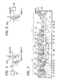
- Fig. 1 is a sectional view showing an embodiment of the present invention.
- Figs. 2A - 2G are sectional views showing a manufacturing process for the embodiment in Fig. 1.
- Fig. 3 is a sectional view of another embodiment of the present invention.
- Figs. 4A and 4B are sectional views showing some steps of a manufacturing process for the embodiment in Fig. 3.
- Figs. 5 and 6 are circuit diagrams showing examples of input and output circuits to which the present invention is applied, respectively.
- Fig. 7 is a sectional view showing still another embodiment of the present invention.
- Fig. 1 shows an embodiment in which the present invention is applied to a semiconductor device, for example, a D-RAM constructed of complementary MOSFETs. A
region 1 is a region (input/output circuit region) in which an element for an input/output circuit is formed, while aregion 2 is a region (internal circuit region) in which elements constituting an internal circuit other than a memory cell are formed. The figure illustrates the sections of the respective elements. - An NMOSFET 11 is formed as the element of the input/
output circuit 1 on asemiconductor substrate 10 made of a P-type silicon single crystal. An NMOSFET 12 and a P-channel MOSFET (hereinbelow, termed 'PMOSFET') 13 are respectively formed as the elements of theinternal circuit 2 on thesubstrate 10 and an N-type well 14 provided therein. The individual MOSFETs are insulated from one another by a field insulator film (Si02) 15 which is an element isolating insulator film. - The NMOSFET 11 comprises a
gate electrode 17 made of polycrystalline silicon, which is formed on a gate insulator film (Si02) 16, and N-type regions 18 as source and drain regions, which are provided in the main surface of thesubstrate 10. Side wall spacers (insulator films) 22 made of Si02 are formed on both the sides of thegate electrode 17 by the.low-pressure CVD process. However, theMOSFET 11 has no LDD structure. Each of the N-type regions 18 is composed of a region (low concentration phosphorus region) 19 which is doped with phosphorus at a low concentration, and a region (high concentration phosphorus region) 20 which is doped with phosphorus at a high concentration. In case of this example, the concentrations of therespective phosphorus regions phosphorus region 20 is set at a concentration of 1 - 20 x 10 19 cm-3 or above. The concentration of thephosphorus region 20 needs to be, at least, higher than that of aphosphorus region 26 to be described later. The inventors have verified that, even when the phosphorus regions of such a high concentration are used as the source and drain regions, the appearance of hot carriers is little, while a strength against electrostatic destruction increases, as will be stated later. In addition, the , depths of junctions which therespective regions substrate 10 are set to 0.2 µm and 0.5 µm. The highconcentration phosphorus regions 20 have their inner ends diffused to positions under both the ends of thegate electrode 17, into the shape in which they encompass the lowconcentration phosphorus regions 19 therein. - The NMOSFET 12 comprises a
gate electrode 23 made of polycrystalline silicon on agate insulator film 16, and N-type regions 24 as source and drain regions.Side wall spacers 25 are formed on both the sdies of thegate electrode 23. Each of the N-type regions 24 is composed of the lowconcentration phosphorus region 26, and a region (arsenic region) 27 which is doped with arsenic at a high concentration. In particular, thearsenic region 27 is formed so as to be apart from a projection of thegate electrode 23 in the main surface of thesubstrate 10 by theside wall spacer 25, and the lowconcentration phosphorus region 26 is formed so as to extend to under theside wall spacer 25. Thus, the so-called LDD structure is established. The concentration of the lowconcentration phosphorus region 26 is at most 10 13 cm-2 (approximately 1 x 10 18 cm-3), and that of thearsenic region 27 is 5 - 10 x 1015 cm-2 (1 - 4 x 10 20 cm-3). The depths of junctions which therespective regions substrate 10 are 0.2 µm and 0.2 - 0.3 pm. - The
PMOSFET 13 comprises agate electrode 28 made of polycrystalline silicon on agate insulator film 16, and P-type regions 29 as source and drain regins formed in the N-type well 14. In this example, thePMOSFET 13 is not of the LDD structure. The P-type regions 29 are formed by doping with boron at a concentration of approximately 5 x 1015 cm-2. -
Layers regions gate electrodes - Fig. 5 is a diagram showing an input circuit, while Fig. 6 is a diagram showing an output circuit, and they exemplify the input/
output circuits 1 respectively. As seen from Figs. 5 and 6, the input/output circuits 1 are circuits which are connected to bonding pads BP. NMOSFETs QN1 - QN3 and PMOSFETs QP1, QP2 are respectively put into the same structures as those of theNMOSFET 11 and thePMOSFET 13. Theinternal circuit 2 includes a portion except for the input/output circuits 1 and the memory cell, in other words, a circuit such as decoder, sense amplifier, main amplifier or any of various signal generators. - In the present embodiment, the NMOSFET of the memory cell is put into the same structure as that of the NMOSFET I
- According to this construction, in the
NMOSFET 12 in theinternal circuit 2, the N-type region 24 is formed into the LDD structure by thearsenic region 27 and the lowconcentration phopshorus region 26, so that an electric field at the edge of thedrain region 24 can be moderated to suppress the appearance of hot carriers. As a result, the fluctuation of a threshold voltage can be prevented to enhance the reliability of characteristics in theinternal circuit 2. - On the other hand, in the
NMOSFET 11 of the input/output circuit 1, the source or drain region (N-type region) 18 is formed of the highconcentration phosphorus region 20 encompassing the lowconcentration phosphorus region 19, so that the reverse breakdown voltage of the junction between the highconcentration phosphorus region 20 and thesubstrate 10 becomes small. Thus, the destruction voltage of the gate insulator film against electrostatic destruction can be enhanced. - By setting the source and drain
regions 18 at the high impurity concentration, the electric field strength is raised. Since, however, the impurity is phosphorus, the impurity concentration gradient is gentle, and hence, the appearance of hot carriers as in the case of arsenic is not involved. Of course, in the input/output circuits, the influences of the hot carriers are originally little on the basis of the relations between element sizes and voltages to be applied. - Further, owing to the use of the
silicide layer 33, it is possible to reduce the resistance of thesemiconductor region 18 and to raise the operating speed of the element even when phosphorus is employed as the impurity. - Next, a method of manufacturing the semiconductor device of the above construction will be described with reference to Figs. 2A - 2G.
- First, as shown in Fig. 2A, an N-
type well 14 is formed in asemiconductor substrate 10 made of a P-type silicon single crystal, and an element isolating insulator film (field insulator film) 15 and agate insulator film 16 are formed. Polycrystalline silicon is deposited on the whole surface of the substrate by CVD, and it is patterned to formgate electrodes respective MOSFETs - Subsequently, as shown in Fig. 2B, under the state under which the portion of the
PMOSFET 13 is masked by aphotoresist film 40, phosphorus at a low concentration (10 13 cm-2 or less) is ion-implanted into the whole surface by employing thegate electrodes layers 41 are formed. At this time, an input/output circuit domain 1 may well be covered with thephotoresist film 40 so as to prevent the phosphorus from being introduced into the source and drain regions of theNMOSFET 11. - After removing the
photoresist film 40, the resultant structure is annealed thereby to form lowconcentration phosphorus regions - The Si02 film 42 is etched by reactive ion etching (RIE), whereby
side wall spacers gate electrodes - Next, as shown in Fig. 2E, under the state under which an
internal circuit region 2, namely, the portion of theNMOSFET 12 as well as the portion of thePMOSFET 13 is masked by aphotoresist film 43, phosphorus at a high concentration (1 - 10 x 1015 cm-2) is ion-implanted by employing thegate electrode 17 and theside wall spacers 22 as a mask. Thus, layers 44 ion-implanted with the high concentration of phosphorus are formed. - After removing the
photoresist film 43, the resultant structure is annealed thereby to form source and drainregions 18 made up of highconcentration phosphorus regions 20 encompassing the lowconcentration phosphorus regions 19 as shown in Fig. 2F. - Thereafter, as shown in Fig. 2F, under the state under which the
PMOSFET 13 and the input/output circuit region 1 are masked by aphotoresist film 45, arsenic is ion-implanted at a concentration of 5 - 10 x 1015 cm -2 by employing thegate electrode 23 and theside wall spacers 25 as a mask. Thus, arsenic ion-implantedlayers 46 are formed for theNMOSFET 12. - By annealing after the removal of the
photoresist film 45,arsenic regions 27 are formed as shown in Fig. 2G. That is, the source and drainregions 24 of theNMOSFET 12 of theinternal circuit 2 are finished up as the LDD structures. - Subsequently, as shown in Fig. 2G, under the state under which the
NMOSFETs photoresist film 47, boron (B) is ion-implanted at a concentration of 5 x 10 15 cm -2 by employing thegate electrode 28 and theside wall spacers 30 as a mask. Thus, boron- implanted layers are formed. By annealing after the removal of thephotoresist film 47, P -type regions 29 as source and drain regions are formed. Thereafter, the parts of theinsulator film 16 on the source and drain regions are removed. Subsequently, a metal film of molybdenum (Mo) or the like is formed on the whole surface of the resultant substrate and is heat-treated into a silicide, and the unreacted parts of the metal film are removed, whereby silicide layers 33 and 34 are formed. - Thenceforth, an
inter-layer insulator film 31,aluminumwiring 32 and final passivation film (not shown) are formed by well-known processes, whereby the semiconductor device in Fig. 1 can be completed. - With this method, the NMOSFET of the input/output circuit can be readily formed merely by adding the masking step of the
photoresist film 43 and the doping step of the high concentration phosphorus as shown in Fig. 2E, to the steps of fabricating the NMOSFET (12) of the LDD structure. Besides, in forming the highconcentration phosphorus regions 20, theside wall spacers 22 are utilized, and hence, the highconcentration phosphorus regions 20 can be formed into a required depth. Also, the channel length can be readily formed into a required length, and increase in the channel length is not incurred, which is effective for microminiaturization. - Fig. 3 shows another embodiment of the present invention. In the figure, the same portions as in Fig. 1 are assigned the same symbols, and they shall not be repeatedly explained.
- In this example, each of N-
type regions 18A as the source and drain regions of theNMOSFET 11A of an input/output circuit 1 comprises a lowconcentration phosphorus region 19, a highconcentration phosphorus region 20 so as to substantially encompass theregion 19, and anarsenic region 21 which is formed on the surface side of theregion 20 and.shallower than thisregion 20 and to be apart from agate electrode 17. The concentrations of thephosphorus regions arsenic region 21 is the same as that of thearsenic region 27 of theNMOSFET 12 of aninternal circuit 2. The depths of therespective regions - A method of manufacturing this semiconductor device is as follows. First, the steps of Fig. 2A - Fig. 2E in the foregoing example are carried out. Thereafter, as shown in Fig. 4A, under the state under which only the
PMOSFET 12 of theinternal circuit 2 is covered with a mask of photoresist 50, arsenic is ion-implanted at a concentration of 5 - 10 x 1015 cm-2. Arsenic ion-implantedlayers 51 formed for both theNMOSFETs arsenic regions corresponding gate electrodes drain regions 18A is obtained in theNMOSFET 11A, and the LDD structures are obtained in theNMOSFET 12. - Subsequently, as shown in Fig. 4B, the
NMOSFETs photoresist film 52, and if necessary,side wall spacers 30 are etched and removed, whereupon boron is ion-implanted. By subsequent annealing, source and drainregions 29 are formed. - Thereafter, an
inter-layer insulator film 31,aluminum wiring 32 and final passivation film are formed, whereby the semiconductor device in Fig. 3 is finished up. - According to this example, the
NMOSFET 12 of theinternal circuit 2 is put into the LDD construction as in the preceding example, so that the appearance of hot carriers is suppressed. On the other hand, in theNMOSFET 11A of the input/output circuit, the main constituents of the source anddrain regions 18A are the highconcentration phosphorus regions 20 extended to both the ends of thegate electrode 17, so that the electrostatic destruction voltage can be enhanced. Moreover, theregions 20 have the high impurity concentration but.use phosphorus, so that the lowering of the hot carrier generation can be suppressed. - Further, since the
arsenic regions 21 apart from the gate electrode are included in the source anddrain regions 18A, the overlaps of the highconcentration phosphorus regions 20 with thegate electrode 17 can be made smaller than in the preceding example, and the transconductance can be enhanced owing to reduction in the junction capacitances. Of course, the operating speed can also be raised by the lowered resistances of the source anddrain regions 18A owing to thearsenic regions 21. - Even in a case where the high
concentration phosphorus regions 20 do not get to both the sides of thegate electrode 17, the lowconcentration phosphorus regions 19 previously formed have been formed by utilizing thegate electrode 17 and reliably extend to under this gate electrode, so that the MOS structure is not spoilt. - According to the present invention, the following effects are produced.
- In a semiconductor device whose internal circuit has a MOSFET of the LDD structure, the source and drain regions of a MOSFET for an input/output circuit are so constructed as to be doped with phosphorus at a high concentration, so that the electrostatic destruction voltage can be enhanced.
- Since source and drain regions are constructed by the use of phosphorus at a high concentration, the concentration gradient is gentle in spite of the high impurity concentration, and the apperance of hot carriers can be suppressed.
- Since the concentration of phosphorus is made as high as 1 - 20 x 1019 cm-3, the appearance of hot carriers can be suppressed, and the electrostatic destruction voltage can be enhanced.
- Only an input/output circuit is provided with regions made by the use of a high concentration of phosphorus, and the others are put into the LDD structures, so that even when the junction capacitances between a substrate and the phosphorus regions increase, the operating speed of the whole IC does not lower.
- Since source and drain regions are formed with arsenic regions, resistances can be reduced to achieve a raised speed.
- Since source and drain regions are formed with silicide layers, resistances can be reduced to achieve a raised speed.
- Since source and drain regions are formed with arsenic regions a part with respect to a gate electrode, the overlaps between phosphorus regions and the gate electrode can be diminished, and junction capacitances can be reduced to enhance a transconductance.
- Since the overlaps between a gate electrode and high concentration phosphorus regions can be diminished, a gate length relative to an effective gate length is shortened, which is effective for the microminiaturization of an element.
- Under the state under which at least an internal circuit is masked, doping with a high concentration of phosphorus is carried out by utilizing side wall spacers, whereupon doping with arsenic is carried out for at least the internal circuit by utilizing the side wall spacers. Thus, the LDD structures can be formed in the internal circuit, and source and drain regions of the high concentration of phosphorus can be formed in an input/output circuit. A semiconductor device of the present invention can be readily manufactured by adding the step of the masking and the step of the doping with the high concentration of phosphorus, to a process for manufacturing an NMOSFET of the LDD structure.
- An impurity is introduced by doping beforehand with a gate electrode used as a mask. Therefore, even when the diffusion of a high concentration of phosphorus is insufficient in case of doping with the high concentration of phosphorus, the MOS structure is not spoilt.
- While, in the above, the invention made by the inventors has been concretely described in conjunction with embodiments, it is needless to say that the present invention is not restricted to the foregoing embodiments but that it can be variously modified within a scope not departing from the purport thereof.
- The present invention is effective for a MOSFET, QN1 or QN3 whose drain is connected to a bonding pad, especially a bonding pad to which an input or output signal is applied. The reason is that electrostatic breakdown is liable to occur in a circuit connected to the bonding pad to which the input or output signal is applied.
- Accordingly, the MOSFET QN2 in Fig. 5 need not be put into the same structure as that of the
MOSFET 11. To the contrary, the present invention is also applicable to an NMOSFET constituting a circuit of the next stage which is connected to an inverter INV1 or INV2 constructed of the MOSFET QN1 or QN3. Further, it is possible that only the drain region of an N-channel MOSFET such as the MOSFET QN1 or QN3 is put into the structure conforming with the present invention. - The low
impurity concentration regions 19 in theMOSFET 11 can be omitted. As shown in Fig. 7, each of the source and drainregions 18 of theMOSFET 11 is made up of only thephosphorus region 20 of high impurity concentration. This can be achieved in such a way that the resistmask 40 shown in Fig. 2B is formed so as to cover the input/output circuit domain 1. That is, the number of manufacturing steps does not increase in a CMOSIC. In an IC (NMOSIC) which is constructed of NMOSFETs without having thePMOSFET 13, a masking step needs to be added. - As shown in Fig. 7, the
layers - An input protective resistor'R shown in Fig. 5 can be formed by extending the source or drain
region 18 of theMOSFET 11. In case of forming a resistor R made of a semiconductor region which is identical and continuous to theregion 18, the structure shown in Fig. 7 is desirable. That is, the source and drainregions 18 of theMOSFET 11 are constructed only of thephosphorus regions 20. The resistor R is formed by extending eitherphosphorus region 20. In order to bring the sheet resistance of theregion 20 to a proper value, thesilicide layer 33 is not formed. For the same reason, at least thearsenic region 27 is not formed. Accordingly, the resistor R can be formed in a small area. One end of the resistor R is connected to the bonding pad BP which is made of thealuminum layer 32. - While, in the above, the invention made by the inventors has been chiefly described on the applications to semiconductor devices of the CMOS type which form the background field of utilization, it is not restricted thereto. The present invention is applicable to a memory IC and also a logic IC other than a DRAM as long as a MOSFET of the LDD structure is included in an internal structure. Further, it is applicable, not only to CMOSICs, but also to NMOSICs. The LDD structure in the present invention may include, at least, a first semiconductor region has a high impurity concentration, and a second semiconductor region which has an impurity concentration lower than that of the first semiconductor region and which is formed closer to a channel side (gate electrode side) than the first semiconductor region. The first semiconductor region need not be deeper than the second semiconductor region. A bonding pad includes, not only a pad for wire bonding, but also a pad for bonding which utilizes a bump electrode or the like. Various semiconductor regions may well be opposite in conductivity type to the foregoing. The concentrations of phosphorus and arsenic can be variously altered within the scope of the purport of the present invention.
Claims (14)
wherein said first semiconductor region (27) is defined by said gate electrode (23) of said first MOSFET (12) and said side wall spacers (25), and said second semiconductor region (26) is defined by said gate electrode (23) of said first MOSFET (12).
Applications Claiming Priority (2)
| Application Number | Priority Date | Filing Date | Title |
|---|---|---|---|
| JP16508/85 | 1985-02-01 | ||
| JP60016508A JPH0695563B2 (en) | 1985-02-01 | 1985-02-01 | Semiconductor device |
Publications (3)
| Publication Number | Publication Date |
|---|---|
| EP0189914A2 true EP0189914A2 (en) | 1986-08-06 |
| EP0189914A3 EP0189914A3 (en) | 1987-04-15 |
| EP0189914B1 EP0189914B1 (en) | 1992-05-06 |
Family
ID=11918210
Family Applications (1)
| Application Number | Title | Priority Date | Filing Date |
|---|---|---|---|
| EP86101166A Expired - Lifetime EP0189914B1 (en) | 1985-02-01 | 1986-01-29 | Semiconductor integrated circuit device and method of manufacturing the same |
Country Status (7)
| Country | Link |
|---|---|
| US (1) | US4717684A (en) |
| EP (1) | EP0189914B1 (en) |
| JP (1) | JPH0695563B2 (en) |
| KR (1) | KR930001560B1 (en) |
| CN (1) | CN1007681B (en) |
| DE (1) | DE3685124D1 (en) |
| HK (1) | HK51294A (en) |
Cited By (9)
| Publication number | Priority date | Publication date | Assignee | Title |
|---|---|---|---|---|
| EP0266768A1 (en) * | 1986-11-07 | 1988-05-11 | Kabushiki Kaisha Toshiba | Manufacturing method for forming a MOS transistor by self-alignment of the source/drain regions |
| EP0356039A1 (en) * | 1988-08-19 | 1990-02-28 | Seiko Epson Corporation | MOS semiconductor integrated circuit |
| EP0387944A1 (en) * | 1989-03-13 | 1990-09-19 | Koninklijke Philips Electronics N.V. | Semiconductor device provided with a protection circuit |
| EP0444686A1 (en) * | 1990-03-02 | 1991-09-04 | Kabushiki Kaisha Toshiba | Semiconductor device having increased elctrostatic breakdown voltage |
| EP0470371A3 (en) * | 1990-07-06 | 1992-07-01 | Kabushiki Kaisha Toshiba | Semiconductor device with input protection circuit of high withstand voltage |
| EP0516146A1 (en) * | 1991-05-29 | 1992-12-02 | Nec Corporation | Semiconductor integrated circuit having improved protection element |
| DE4223313A1 (en) * | 1991-07-16 | 1993-01-21 | Mitsubishi Electric Corp | SEMICONDUCTOR DEVICE AND METHOD FOR THE PRODUCTION THEREOF |
| EP0675543A3 (en) * | 1994-03-31 | 1996-10-16 | Seiko Instr Inc | Semiconductor device comprising protection means and associated manufacturing method. |
| WO1997016852A1 (en) * | 1995-10-30 | 1997-05-09 | Advanced Micro Devices, Inc. | A semiconductor circuit including non-esd transistors with reduced degradation due to an impurity implant and method for making same |
Families Citing this family (37)
| Publication number | Priority date | Publication date | Assignee | Title |
|---|---|---|---|---|
| JP3437863B2 (en) * | 1993-01-18 | 2003-08-18 | 株式会社半導体エネルギー研究所 | Method for manufacturing MIS type semiconductor device |
| US5247199A (en) * | 1986-01-15 | 1993-09-21 | Harris Corporation | Process for forming twin well CMOS integrated circuits |
| US5215936A (en) * | 1986-10-09 | 1993-06-01 | Kabushiki Kaisha Toshiba | Method of fabricating a semiconductor device having a lightly-doped drain structure |
| US4978628A (en) * | 1986-11-19 | 1990-12-18 | Teledyne Industries, Inc. | Drail-well/extension high voltage MOS transistor structure and method of fabrication |
| US4764482A (en) * | 1986-11-21 | 1988-08-16 | General Electric Company | Method of fabricating an integrated circuit containing bipolar and MOS transistors |
| US4764477A (en) * | 1987-04-06 | 1988-08-16 | Motorola, Inc. | CMOS process flow with small gate geometry LDO N-channel transistors |
| JPH07107919B2 (en) * | 1987-05-07 | 1995-11-15 | 松下電子工業株式会社 | Semiconductor integrated circuit |
| JPS6455855A (en) * | 1987-08-27 | 1989-03-02 | Mitsubishi Electric Corp | Complementary type field effect transistor |
| US5086008A (en) * | 1988-02-29 | 1992-02-04 | Sgs-Thomson Microelectronics S.R.L. | Process for obtaining high-voltage N channel transistors particularly for EEPROM memories with CMOS technology |
| US4874713A (en) * | 1989-05-01 | 1989-10-17 | Ncr Corporation | Method of making asymmetrically optimized CMOS field effect transistors |
| JP2625602B2 (en) * | 1991-01-18 | 1997-07-02 | インターナショナル・ビジネス・マシーンズ・コーポレイション | Manufacturing process of integrated circuit devices |
| US5268317A (en) * | 1991-11-12 | 1993-12-07 | Siemens Aktiengesellschaft | Method of forming shallow junctions in field effect transistors |
| AU5669794A (en) * | 1992-12-11 | 1994-07-04 | Intel Corporation | A mos transistor having a composite gate electrode and method of fabrication |
| US5953582A (en) * | 1993-02-10 | 1999-09-14 | Seiko Epson Corporation | Active matrix panel manufacturing method including TFTS having variable impurity concentration levels |
| US5838033A (en) * | 1993-09-08 | 1998-11-17 | Lucent Technologies Inc. | Integrated circuit with gate conductor defined resistor |
| CN1881620B (en) * | 1993-10-01 | 2010-06-23 | 株式会社半导体能源研究所 | Semiconductor device and a manufacturing method for the same |
| US5472887A (en) * | 1993-11-09 | 1995-12-05 | Texas Instruments Incorporated | Method of fabricating semiconductor device having high-and low-voltage MOS transistors |
| JP2682425B2 (en) * | 1993-12-24 | 1997-11-26 | 日本電気株式会社 | Method for manufacturing semiconductor device |
| US5432105A (en) * | 1994-09-19 | 1995-07-11 | United Microelectronics Corporation | Method for fabricating self-aligned polysilicon contacts on FET source/drain areas |
| US5672527A (en) * | 1996-03-08 | 1997-09-30 | United Microelectronics Corp. | Method for fabricating an electrostatic discharge protection circuit |
| US6037227A (en) * | 1997-06-03 | 2000-03-14 | United Microelectronics Corp. | Method of making high density mask ROM having a two level bit line |
| US6603180B1 (en) * | 1997-11-28 | 2003-08-05 | Advanced Micro Devices, Inc. | Semiconductor device having large-area silicide layer and process of fabrication thereof |
| JP3149937B2 (en) * | 1997-12-08 | 2001-03-26 | 日本電気株式会社 | Semiconductor device and method of manufacturing the same |
| FR2773266B1 (en) * | 1997-12-31 | 2001-11-09 | Sgs Thomson Microelectronics | ELECTRONIC STRUCTURE COMPRISING HIGH AND LOW VOLTAGE TRANSISTORS AND CORRESPONDING METHOD OF MANUFACTURING |
| US5953601A (en) * | 1998-02-17 | 1999-09-14 | Taiwan Semiconductor Manufacturing Company, Ltd. | ESD implantation scheme for 0.35 μm 3.3V 70A gate oxide process |
| US5897348A (en) * | 1998-03-13 | 1999-04-27 | Texas Instruments - Acer Incorporated | Low mask count self-aligned silicided CMOS transistors with a high electrostatic discharge resistance |
| US5998247A (en) * | 1998-04-09 | 1999-12-07 | Texas Instruments - Acer Incorporated | Process to fabricate the non-silicide region for electrostatic discharge protection circuit |
| JP2001127270A (en) * | 1999-10-27 | 2001-05-11 | Nec Corp | Semiconductor device and manufacturing method therefor |
| KR100308087B1 (en) * | 1999-11-26 | 2001-11-05 | 박종섭 | Electrostatic discharge protection circuit and method for fabricating the same |
| US6509223B2 (en) * | 2001-01-19 | 2003-01-21 | United Microelectronics Corp. | Method for making an embedded memory MOS |
| EP1263033A1 (en) * | 2001-05-24 | 2002-12-04 | Texas Instruments Inc. | Fabrication of analog core CMOS, digital core CMOS, and I/O CMOS transistors |
| US6563175B2 (en) * | 2001-09-24 | 2003-05-13 | Texas Instruments Incorporated | NMOS ESD protection device with thin silicide and methods for making same |
| KR100574948B1 (en) * | 2003-08-23 | 2006-04-28 | 삼성전자주식회사 | Semiconductor memory device with reduced parasitic capacitance and manufacturing method thereof |
| JP2006019511A (en) * | 2004-07-01 | 2006-01-19 | Fujitsu Ltd | Semiconductor device and manufacturing method thereof |
| US7585737B2 (en) | 2006-11-30 | 2009-09-08 | Taiwan Semiconductor Manufacturing Company, Ltd. | Method of manufacturing double diffused drains in semiconductor devices |
| US8026135B2 (en) * | 2007-08-15 | 2011-09-27 | Texas Instruments Incorporated | Formation of shallow junctions by diffusion from a dielectric doped by cluster or molecular ion beams |
| JP5778900B2 (en) * | 2010-08-20 | 2015-09-16 | 富士通セミコンダクター株式会社 | Manufacturing method of semiconductor device |
Family Cites Families (17)
| Publication number | Priority date | Publication date | Assignee | Title |
|---|---|---|---|---|
| US3731161A (en) * | 1970-09-05 | 1973-05-01 | Nippon Electric Co | Semiconductor integrated circuit |
| JPS5368581A (en) * | 1976-12-01 | 1978-06-19 | Hitachi Ltd | Semiconductor device |
| FR2445617A1 (en) * | 1978-12-28 | 1980-07-25 | Ibm France | IMPROVED BREAKDOWN VOLTAGE RESISTANCE ACHIEVED BY DOUBLE ION IMPLANTATION IN A SEMICONDUCTOR SUBSTRATE AND MANUFACTURING METHOD THEREOF |
| US4325180A (en) * | 1979-02-15 | 1982-04-20 | Texas Instruments Incorporated | Process for monolithic integration of logic, control, and high voltage interface circuitry |
| JPS5696850A (en) * | 1979-12-30 | 1981-08-05 | Fujitsu Ltd | Semiconductor device and manufacture thereof |
| JPS5715459A (en) * | 1980-07-01 | 1982-01-26 | Fujitsu Ltd | Semiconductor integrated circuit |
| US4356623A (en) * | 1980-09-15 | 1982-11-02 | Texas Instruments Incorporated | Fabrication of submicron semiconductor devices |
| US4475280A (en) * | 1980-12-24 | 1984-10-09 | General Electric Company | Method of making an integrated circuit incorporating low voltage and high voltage semiconductor devices |
| JPS5833870A (en) * | 1981-08-24 | 1983-02-28 | Hitachi Ltd | Semiconductor device |
| US4590663A (en) * | 1982-02-01 | 1986-05-27 | Texas Instruments Incorporated | High voltage CMOS technology with N-channel source/drain extensions |
| JPS59920A (en) * | 1982-06-23 | 1984-01-06 | Fujitsu Ltd | Manufacture of semiconductor device |
| JPS5972759A (en) * | 1982-10-20 | 1984-04-24 | Toshiba Corp | Semiconductor device and manufacture thereof |
| US4466177A (en) * | 1983-06-30 | 1984-08-21 | International Business Machines Corporation | Storage capacitor optimization for one device FET dynamic RAM cell |
| JPS6072272A (en) * | 1983-09-28 | 1985-04-24 | Toshiba Corp | Manufacture of semiconductor device |
| JPH0693494B2 (en) * | 1984-03-16 | 1994-11-16 | 株式会社日立製作所 | Method for manufacturing semiconductor integrated circuit device |
| US4577391A (en) * | 1984-07-27 | 1986-03-25 | Monolithic Memories, Inc. | Method of manufacturing CMOS devices |
| FR2571178B1 (en) * | 1984-09-28 | 1986-11-21 | Thomson Csf | INTEGRATED CIRCUIT STRUCTURE HAVING HIGH VOLTAGE HOLD CMOS TRANSISTORS, AND MANUFACTURING METHOD THEREOF |
-
1985
- 1985-02-01 JP JP60016508A patent/JPH0695563B2/en not_active Expired - Lifetime
-
1986
- 1986-01-13 KR KR1019860000142A patent/KR930001560B1/en not_active Expired - Fee Related
- 1986-01-29 DE DE8686101166T patent/DE3685124D1/en not_active Expired - Lifetime
- 1986-01-29 EP EP86101166A patent/EP0189914B1/en not_active Expired - Lifetime
- 1986-01-31 CN CN86100841A patent/CN1007681B/en not_active Expired
- 1986-02-03 US US06/825,587 patent/US4717684A/en not_active Expired - Lifetime
-
1994
- 1994-05-19 HK HK51294A patent/HK51294A/en not_active IP Right Cessation
Cited By (13)
| Publication number | Priority date | Publication date | Assignee | Title |
|---|---|---|---|---|
| EP0266768A1 (en) * | 1986-11-07 | 1988-05-11 | Kabushiki Kaisha Toshiba | Manufacturing method for forming a MOS transistor by self-alignment of the source/drain regions |
| EP0356039A1 (en) * | 1988-08-19 | 1990-02-28 | Seiko Epson Corporation | MOS semiconductor integrated circuit |
| EP0387944A1 (en) * | 1989-03-13 | 1990-09-19 | Koninklijke Philips Electronics N.V. | Semiconductor device provided with a protection circuit |
| US5239194A (en) * | 1990-03-02 | 1993-08-24 | Kabushiki Kaisha Toshiba | Semiconductor device having increased electrostatic breakdown voltage |
| EP0444686A1 (en) * | 1990-03-02 | 1991-09-04 | Kabushiki Kaisha Toshiba | Semiconductor device having increased elctrostatic breakdown voltage |
| EP0470371A3 (en) * | 1990-07-06 | 1992-07-01 | Kabushiki Kaisha Toshiba | Semiconductor device with input protection circuit of high withstand voltage |
| US5210436A (en) * | 1990-07-06 | 1993-05-11 | Kabushiki Kaisha Toshiba | Semiconductor device with input protection circuit of high withstand voltage |
| EP0516146A1 (en) * | 1991-05-29 | 1992-12-02 | Nec Corporation | Semiconductor integrated circuit having improved protection element |
| DE4223313A1 (en) * | 1991-07-16 | 1993-01-21 | Mitsubishi Electric Corp | SEMICONDUCTOR DEVICE AND METHOD FOR THE PRODUCTION THEREOF |
| US5327000A (en) * | 1991-07-16 | 1994-07-05 | Mitsubishi Denki Kabushiki Kaisha | Semiconductor device interconnected to analog IC driven by high voltage |
| EP0675543A3 (en) * | 1994-03-31 | 1996-10-16 | Seiko Instr Inc | Semiconductor device comprising protection means and associated manufacturing method. |
| US6097064A (en) * | 1994-03-31 | 2000-08-01 | Seiko Instruments Inc. | Semiconductor device and manufacturing method thereof |
| WO1997016852A1 (en) * | 1995-10-30 | 1997-05-09 | Advanced Micro Devices, Inc. | A semiconductor circuit including non-esd transistors with reduced degradation due to an impurity implant and method for making same |
Also Published As
| Publication number | Publication date |
|---|---|
| CN1007681B (en) | 1990-04-18 |
| KR860006840A (en) | 1986-09-15 |
| EP0189914B1 (en) | 1992-05-06 |
| JPS61177769A (en) | 1986-08-09 |
| JPH0695563B2 (en) | 1994-11-24 |
| HK51294A (en) | 1994-05-27 |
| KR930001560B1 (en) | 1993-03-04 |
| EP0189914A3 (en) | 1987-04-15 |
| US4717684A (en) | 1988-01-05 |
| CN86100841A (en) | 1986-07-30 |
| DE3685124D1 (en) | 1992-06-11 |
Similar Documents
| Publication | Publication Date | Title |
|---|---|---|
| EP0189914B1 (en) | Semiconductor integrated circuit device and method of manufacturing the same | |
| US5436484A (en) | Semiconductor integrated circuit device having input protective elements and internal circuits | |
| US4052229A (en) | Process for preparing a substrate for mos devices of different thresholds | |
| EP0164449A2 (en) | Process for producing a semiconductor integrated circuit device including a MISFET | |
| EP0248292B1 (en) | Semiconductor device having a high breakdown voltage | |
| US5610089A (en) | Method of fabrication of semiconductor integrated circuit device | |
| US5838033A (en) | Integrated circuit with gate conductor defined resistor | |
| KR950012705A (en) | Transistor of electrostatic discharge protection circuit and its manufacturing method | |
| US6278162B1 (en) | ESD protection for LDD devices | |
| US4960725A (en) | Semiconductor device and manufacturing process for providing device regions on the semiconductor device and isolation regions to isolate the device regions from each other. | |
| JP2894966B2 (en) | Asymmetric MOS semiconductor device, method of manufacturing the same, and electrostatic discharge protection circuit including the semiconductor device | |
| US5675168A (en) | Unsymmetrical MOS device having a gate insulator area offset from the source and drain areas, and ESD protection circuit including such a MOS device | |
| EP0144248A2 (en) | Mis type semiconductor device element on a semiconductor substrate having a well region | |
| JP3425043B2 (en) | Method for manufacturing MIS type semiconductor device | |
| KR930001561B1 (en) | Semiconductor integrated circuit device | |
| KR100428931B1 (en) | Semiconductor device and method of manufacturing the same | |
| JP2993784B2 (en) | Semiconductor device and manufacturing method thereof | |
| JP2841467B2 (en) | Method for manufacturing MOS type semiconductor device | |
| JPS62265765A (en) | Semiconductor device and manufacture thereof | |
| JPH0817206B2 (en) | Semiconductor device | |
| KR100214860B1 (en) | Electrostatic discharge protecting structure for semiconductor device and manufacture thereof | |
| JPS627710B2 (en) | ||
| JP3448465B2 (en) | Method for manufacturing semiconductor device | |
| JPH0278228A (en) | Field-effect transistor | |
| JPH0456280A (en) | Semiconductor device and manufacture thereof |
Legal Events
| Date | Code | Title | Description |
|---|---|---|---|
| PUAI | Public reference made under article 153(3) epc to a published international application that has entered the european phase |
Free format text: ORIGINAL CODE: 0009012 |
|
| AK | Designated contracting states |
Kind code of ref document: A2 Designated state(s): DE FR GB IT |
|
| PUAL | Search report despatched |
Free format text: ORIGINAL CODE: 0009013 |
|
| AK | Designated contracting states |
Kind code of ref document: A3 Designated state(s): DE FR GB IT |
|
| 17P | Request for examination filed |
Effective date: 19870930 |
|
| 17Q | First examination report despatched |
Effective date: 19901123 |
|
| GRAA | (expected) grant |
Free format text: ORIGINAL CODE: 0009210 |
|
| AK | Designated contracting states |
Kind code of ref document: B1 Designated state(s): DE FR GB IT |
|
| REF | Corresponds to: |
Ref document number: 3685124 Country of ref document: DE Date of ref document: 19920611 |
|
| ET | Fr: translation filed | ||
| ITF | It: translation for a ep patent filed | ||
| PLBE | No opposition filed within time limit |
Free format text: ORIGINAL CODE: 0009261 |
|
| STAA | Information on the status of an ep patent application or granted ep patent |
Free format text: STATUS: NO OPPOSITION FILED WITHIN TIME LIMIT |
|
| 26N | No opposition filed | ||
| REG | Reference to a national code |
Ref country code: GB Ref legal event code: IF02 |
|
| PGFP | Annual fee paid to national office [announced via postgrant information from national office to epo] |
Ref country code: GB Payment date: 20021223 Year of fee payment: 18 |
|
| PGFP | Annual fee paid to national office [announced via postgrant information from national office to epo] |
Ref country code: FR Payment date: 20021230 Year of fee payment: 18 |
|
| PGFP | Annual fee paid to national office [announced via postgrant information from national office to epo] |
Ref country code: DE Payment date: 20030310 Year of fee payment: 18 |
|
| PG25 | Lapsed in a contracting state [announced via postgrant information from national office to epo] |
Ref country code: GB Free format text: LAPSE BECAUSE OF NON-PAYMENT OF DUE FEES Effective date: 20040129 |
|
| PG25 | Lapsed in a contracting state [announced via postgrant information from national office to epo] |
Ref country code: DE Free format text: LAPSE BECAUSE OF NON-PAYMENT OF DUE FEES Effective date: 20040803 |
|
| GBPC | Gb: european patent ceased through non-payment of renewal fee |
Effective date: 20040129 |
|
| PG25 | Lapsed in a contracting state [announced via postgrant information from national office to epo] |
Ref country code: FR Free format text: LAPSE BECAUSE OF NON-PAYMENT OF DUE FEES Effective date: 20040930 |
|
| REG | Reference to a national code |
Ref country code: FR Ref legal event code: ST |
|
| PG25 | Lapsed in a contracting state [announced via postgrant information from national office to epo] |
Ref country code: IT Free format text: LAPSE BECAUSE OF NON-PAYMENT OF DUE FEES;WARNING: LAPSES OF ITALIAN PATENTS WITH EFFECTIVE DATE BEFORE 2007 MAY HAVE OCCURRED AT ANY TIME BEFORE 2007. THE CORRECT EFFECTIVE DATE MAY BE DIFFERENT FROM THE ONE RECORDED. Effective date: 20050129 |