EP0190484A2 - Ordinateur numérique à vitesse augmentée et méthode d'augmentation de vitesse - Google Patents
Ordinateur numérique à vitesse augmentée et méthode d'augmentation de vitesse Download PDFInfo
- Publication number
- EP0190484A2 EP0190484A2 EP85307894A EP85307894A EP0190484A2 EP 0190484 A2 EP0190484 A2 EP 0190484A2 EP 85307894 A EP85307894 A EP 85307894A EP 85307894 A EP85307894 A EP 85307894A EP 0190484 A2 EP0190484 A2 EP 0190484A2
- Authority
- EP
- European Patent Office
- Prior art keywords
- microinstruction
- branch
- instruction
- address
- register
- Prior art date
- Legal status (The legal status is an assumption and is not a legal conclusion. Google has not performed a legal analysis and makes no representation as to the accuracy of the status listed.)
- Withdrawn
Links
Images















Classifications
-
- G—PHYSICS
- G06—COMPUTING OR CALCULATING; COUNTING
- G06F—ELECTRIC DIGITAL DATA PROCESSING
- G06F9/00—Arrangements for program control, e.g. control units
- G06F9/06—Arrangements for program control, e.g. control units using stored programs, i.e. using an internal store of processing equipment to receive or retain programs
- G06F9/22—Microcontrol or microprogram arrangements
- G06F9/26—Address formation of the next micro-instruction ; Microprogram storage or retrieval arrangements
- G06F9/262—Arrangements for next microinstruction selection
- G06F9/264—Microinstruction selection based on results of processing
- G06F9/267—Microinstruction selection based on results of processing by instruction selection on output of storage
-
- G—PHYSICS
- G06—COMPUTING OR CALCULATING; COUNTING
- G06F—ELECTRIC DIGITAL DATA PROCESSING
- G06F9/00—Arrangements for program control, e.g. control units
- G06F9/06—Arrangements for program control, e.g. control units using stored programs, i.e. using an internal store of processing equipment to receive or retain programs
- G06F9/22—Microcontrol or microprogram arrangements
- G06F9/28—Enhancement of operational speed, e.g. by using several microcontrol devices operating in parallel
Definitions
- a stored-program computer typically includes a device for storing the memory address, or the equivalent thereof, of the next instruction to be executed by the central processing unit; this device usually takes the form of a register, and is typically called the "program counter", or "PC".
- the program counter typically is loaded with the starting address of a desired sequence of instructions, and is incremented from that point to "point to" successive addresses of the subsequent instructions.
- the next instruction to be executed is typically the next sequential instruction in the memory device. Bowever, some of the instructions may be “branch” or “jump,” instructions, which result in next executing an instruction other than the next sequential instruction. Such other instruction is known as the "target" instruction of a branch.
- a "conditional branch" instruction specifies that a target instruction (other than the next sequential instruction) will be executed if a certain specified condition (such as a machine-state condition or a variable being equal to a certain value) is met. If the specified condition is not met, the next sequential instruction is executed.
- a certain specified condition such as a machine-state condition or a variable being equal to a certain value
- an instruction to be executed is fetched from the memory location indicated by the program counter.
- the program counter is then incremented to point to the next sequential instruction to be fetched. If execution of the current instruction indicates that branching is to occur, the program counter contents are overwritten by the branch address specified by the current branch instruction. Using the program counter to indicate the address in memory of the next instruction, the correct next instruction is then fetched.
- computers typically employ a LIFO (last-in, firat-out) memory, usually called a "stack", to store return addresses (i.e., the addresses of instructions following call instructions, which are the addresses at which execution is to be resumed after executing return instructions).
- return addresses i.e., the addresses of instructions following call instructions, which are the addresses at which execution is to be resumed after executing return instructions.
- the program counter While executing a call instruction, the program counter contains the address of the next sequential instruction, having been incremented as mentioned above after being used to fetch the call instruction. The program counter contents are then usually placed in the next available location in the stack (often referred to as the "top of the stack"). The program counter is loaded with the address specified in the call instruction as the starting address of the subroutine, and execution of the subroutine proceeds from there.
- the program counter When the return instruction is encountered, the program counter is loaded with the address of the instruction at which execution is to be resumes, i.e. the address of the instruction following the call instruction which invoked the subroutine. This address is found on top of the stack, for it was placed there as part of the execution of the call instruction.
- a stack pointer typically a multibit register with provision for incrementing and decrementing by one.
- a register containing the address of some item is commonly said to "point to” that item.
- the stack pointer initially points to the first location in the stack, is incremented by one whenever anything is placed on the stack, and is decremented by one whenever anything is retrieved from the stack. Thus, the stack pointer always points to the next available location in the stack.
- This scheme allows for "nested subroutine calls”, i.e., for a subroutine to call another subroutine.
- the stack portions of prior art machines typically hold the address of the next memory location to be accessed in the stack. For each memory access, the contents of the stack pointer must be decoded (usually accomplished by gating logic) to select the corresponding memory location. Additional gating must be employed to determine whether the stack has overflowed (i.e., an attempt was made to exceed its capacity) or underflowed (i.e., an attempt was made to retrieve non-existent contents).
- branchi g will be used to denote the situation that exists when the next instruction to be executed is other than the next sequential one, regardless of whether this is because of a branch instruction, a call instruction, or a return instruction.
- Efforts to speed up the operation of digital computers have included such improvements as "instruction prefetching", wherein the next instruction to be executed is fetched from memory while a current instruction is still executing.
- instruction prefetching wherein the next instruction to be executed is fetched from memory while a current instruction is still executing.
- execution of an instruction can commence immediately upon the completion of the execution of the previous instruction and the central processing unit is not delayed while memory accesses, bus transfers, and the like take place.
- a problem in extracting the full benefit from instruction prefetching occurs in conjunction with conditional branch instructions. It usually cannot be known whether a conditional branch is to take place until some point near the end of execution of the conditional branch instruction, by which time the next sequential instruction (not the target instruction) should already have been fetched. A delay then ensues while fetching the target instruction.
- Various approaches have been tried to limit this delay in fetching the target instruction, such as mechanisms for predicting the outcome of a conditional branch (see, for example, U.S. Patent 4,430,706 issued to Sand), or assuming that conditional branches will always be taken (or never be taken), and requiring the programmer to construct his programs in as close conformance as possible to the assumption. (For example, in coding a loop that is to be executed twenty times, the programmer can employ an exit branch that is not taken twenty times and then taken once, or alternatively a return branch that is taken twenty times and then not taken once.)
- This invention is embodied in a microinstruction-controlled microcomputer including a control store for storing microinstructions which may include conditional branch instructions.
- the invention provides a dual prefetch path for prefetching both the next sequential microinstruction and the target microinstruction specified by a branch microinstruction.
- the invention also provides for selecting, prior to the completion of execution of the conditional branch instruction, which of the two prefetched microinstructions is to be executed next. This permits execution of microinstructions without delays attributable to fetching of the next microinstruction, even in the presence of conditional branch instructions.
- FIG. 1 shows the microinstruction fetching and execution portions of a prior art machine employing instruction prefetching.
- Program Counter (PC) 101 is initially loaded with the starting address of a desired sequence of microinstructions by initial load means 102.
- Control store 104 contains sequences of microinstructions.
- control store 104 fetches the microinstruction from the location whose address was received from PC 101, and forwards the fetched microinstruction to prefetch register 105.
- Increment means 103 increments PC 101 so that PC 101 is ready to address the next sequential microinstruction on the next fetch.
- microinstruction register 106 During the next microinstruction cycle the microinstruction from prefetch register 105 is transferred to microinstruction register 106 where it is decoded and then executed by ALU 108.
- ALU denotes "arithmetic and logic unit", that portion of a computer's central processing unit that actually performs the operations specified by the instructions.)
- a microinstruction is to branch (either because it specifies an unconditional branch, or because it specifies a conditional branch and the condition is met) the branch address contained within or specified by a field of the branch microinstruction ia input over lines 109 to PC 101, so that the next prefetch will be of the target microinstruction specified by the branch microinstruction.
- Figure 2 shows the timing that would result when the prior art machine depicted in Figure 1 executes the microinstruction sequence of Table 1.
- microinstruction 100 Assuming that microinstruction 100 has been prefetched prior to cycle 1, it will be in the microinstruction register 106 and will be executed during cycle 1.
- microinstruction 101 will be prefetched from the control store 104 under control of the PC 101, which, as described above, has been incremented to 101 after fetching microinstruction 100. After microinstruction 101 has been prefetched, the PC 101 is incremented to 102.
- Microinstruction 101 will be placed in the prefetch register 105 .
- microiastruction 101 is transferred from the prefetch register 105 to the microinstruction register 106. It is executed during cycle 2.
- microinstruction 102 will be prefetched and the PC 101 will be incremented to 103.
- microinstruction 200 determines that the specified conditional branch is to take place, i.e., the next microinstruction to be executed is microinstruction 200.
- the number "200.” from the branch address field of microinstruction 101 is loaded into the PC 101, overwriting the number "103" to which it had been incremented.
- Microinstruction 200 has not been prefetched-- microinstruction 102 has been prefetched because it was not known at the beginning of cycle 2 that the branch to 200 would take place. (The specified conditions could not be examined until some point during cycle 2.) Thus cycle 3 is lost to the ALU 108, since the microinstruction it should execute during cycle 3 has not yet been fetched from control store 104.
- Cycle 3 must be devoted to prefetching microinstruction 200 from control store 104.
- PC 101 is incremented to 201, which is the instruction that will be fetched during cycle 4.
- Microinstruction 200 is transferred to the microinstruction register 106 at the start of cycle 4 for execution by ALU 108 during cycle 4.
- the prefetch scheme of the present invention which eliminates the problem of lost instruction cycle time due to incorrect prefetches for conditional branches, is shown in high-level block diagram form in Figure 3. (Subsequent figures will disclose more detail.)
- a major difference between the prior art and this invention is the dual prefetch path, comprising prefetch register 308 and prefetch buffer 309.
- every microinstruction is a conditional branch, conditional call, or conditional return microinstruction.
- every instruction has the potential to specify either of two instructions as its successor in execution. Therefore, two microinstructions are prefetched during every microinstruction cycle. In embodiments wherein some microinstructions do not have this potential, it would be possible to prefetch only one microinstruction during the execution of those microinstructions.
- prefetch register 308 receives the next sequential microinstruction from control store 307; during the second half, prefetch buffer 309 receives the branch target microinstruction from control store 307. Either prefetch register 308 or prefetch buffer 309 may load microword register 310 with the microinstruction to be executed next, depending on the determination made during the current execution cycle of whether the branch is to be taken.
- the addresses used to prefetch microinstructions are provided to control store 307 by HUX 306, which may obtain the addresses from any of three sources: (1) branch addresses obtained from (a) the current microinstruction in microword register 310 or (b) from stack 315, one being selected and passed through branch HUX 302 and forwarding circuit 313; (2) a previous branch address stored in branch latch 314, as incremented by branch +1 adder 304 and passed through PC HUX 305; or (3) PC (program counter) 301, as incremented by PC +1 adder 303 and passed through PC MUX 305.
- PC MUX 305 can load PC 301 to ready it for its next uce, loading it with either its former contents as incremented by PC +1 adder 303, or the branch address from branch latch 314 as incremented by branch +1 adder 304. The interactions between these three address source paths and the PC loading path will be discussed in detail below.
- microinstructions fetched by control store 307 are, as mentioned above, brought to microword register 310 either through prefetch buffer 309 or prefetch register 308. Once in microword register 310, they are executed by ALU 312.
- ALU 312, which executes the microinstructions contained in microword register 310, can be a conventional ALU and will not be described herein.
- Control store 307 is accessed twice per microinstruction cycle: once to prefetch the microinstruction that is stored sequentially after the microinstruction which is currently executing, and once to prefetch the branch target microinstruction of the microinstruction that is'currently being executed. At the conclusion of executing the current microinstruction, at which time it will be known whether a conditional branch is to take place, both possible next microinstructions have been prefetched and execution of the correct one of the two can commence without any delay to fetch a different microinstruction.
- Prefetching the next sequential microinstruction is done during the first half of the microinstruction execution cycle, and proceeds in one of two ways, depending on whether the currently executing microinstruction was reached sequentially from a previous microinstruction, or was reached by being a branch target. The reason for this distinction will become evident during the discussion of how branches are effected.
- PC +1 adder 303 increments the address by one so as to denote the next sequential microinstruction.
- the incremented address is selected by PC MUX 305, in response to a timing signal, and passed through MUX 306 to control store 307, which uses that address to prefetch the next sequential microinstruction.
- next sequential microinstruction regardless of whether its address was obtained from branch latch 314 or PC 301, is stored in prefetch register 308 pending the dete ination of whether the currently executing microinstruction is to branch, as discussed below.
- Branch addresses 311, specified in the currently executing microinstruction contained in microword register 310 or obtained from stack 315, are forwarded to branch mux 302 which selects the appropriate one of the branch addresses (in response to the ALU and bused upon the currently executing microinstruction) and forwards it through branch address forwarding circuit 313 and through HUX 306-as the address input to control store 307.
- Control store 307 fetches and applies the 96-bit.branch target microinstruction to the inputs of prefetch buffer 309.
- branch target microinstruction is then available to be gated through prefetch buffer 309 in the event that it is needed; i.e., that the conditional branch specified in the currently executing microinstruction is to be taken.
- the branch address from branch address forwarding circuit 313 is retained in branch latch 314 for possible use during the first half of the next microinstruction cycle.
- ALU 312 determines, from current conditions, whether the currently executing microinstruction is to branch. If it is, then the branch target microinstruction, which is now available at the inputs of prefetch buffer 309, is gated through prefetch buffer 309 and into microword register 310, where ALU 312 will execute it during the next cycle.
- next sequential microinstruction which, as discussed previously, is stored in prefetch register 308, is gated into microword register 310, where ALU 312 will execute it during the next cycle.
- PC MUX 305 at this time loads PC 301 with the address of the next sequential microinstruction, which as previously discussed is either the contents of branch latch 314 incremented by one, or the old PC 301 contents incremented by one.
- branch latch 314 incremented by one
- Figure 4 shows the timing when executing the microinstruction sequence of Table 1 on the microcomputer using the present invention.
- microinstruction cycle 1 microinstruction 100 is executing.
- the microinstruction cycles are each 140 nanoseconds (ns) in duration.
- microinstruction 101 the next sequential microinstruction
- prefetch register 308 the last 70 ns of cycle 1
- microinstruction 400 the target of the conditional branch of microinstruction 100
- prefetch buffer 309 the target of the conditional branch of microinstruction 100
- microinstruction 101 will be transferred from the prefetch register 308 to the microword register 310, and will be the microinstruction to be executed during cycle 2, the next cycle.
- Microinstruction 400 available through prefetch buffer 309, is ignored.
- microinstruction 102 (the next sequential microinstruction) is prefetched to the prefetch register 308, and during the second 70 ns microinstruction 200 (the conditional branch target microinstruction) is prefetched to the prefetch buffer 309.
- the execution logic determines that the conditional branch to microinstruction 200 is to be taken; microinstruction 200 is transferred through the prefetch buffer 309 to the microvord register 310 and thus will be executed during cycle 3.
- Hicroinstruction 102, in prefetch register 308, is ignored. No time is lost between microinstruction cycles because of incorrect prefetches; both possibilities of a branch are always prefetched.
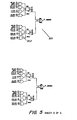
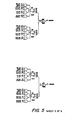
- Figures 5 and 6 together depict the logic of branch MUX 302.
- a MUX (a common designation for "multiplexor") is a device for selecting one of a plurality of signals.
- Branch HUX 302 is used to select one of branch addresses 311. Since control store 307 has a capacity of 4096 locations, a 12-bit address is required to address any of those locations.
- Figures 5 and 6 depict twelve similarly configured logic groups, each for handling a different one of the requisite twelve bits, numbered 00 through 11.
- Group 501 on Figure 5 (for handling bit 02) is deemed to be representative of the twelve logic groups: it has multiple inputs, those inputs being bit 02 of each of branch addresses 311 originating from bit positions of microvord register 310 or from stack 315 as will be discussed further on.
- group 501 selects one of those as the one to output as signal BRADR02.
- Methodologies of laying out instruction sets, including methodologies of specifying branch addresses, are well known in the literature and will not be discussed herein. Designs for combinatorial gating to select one of a plurality of inputs are likewise well known, and will likewise not be discussed herein.
- group 501 produces signal BRADRO2
- all twelve logic groups working in concert produce the twelve bit branch address BRADROO through BRADRII, which is input to branch address forwarding circuit 313, depicted in Figure 10.
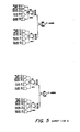
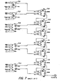
- Figure 7 shows the logic comprising branch latch 314 and branch +1 adder 304.
- Elements 701 through 707 comprise branch latch 314.
- 701 and 702 are single latch circuits
- 703 through 707 are dual latch circuits, yielding a total of 12 latch circuits for containing the twelve-bit address.
- a latch is a bistable circuit which, when its clock input is a logic high will simply pass the state of its data input through to the data output, and which stores the state of the data input at the time its clock input transits to a logic low.
- the tvelve-bit input to branch latch 304 is the address BRADOO through BRADII from branch address forwarding circuit 313 ( Figure 10), which is stored in branch latch 314 and then appears on signal lines BRLOO through BRLII.
- half adders 708 through 718 which comprise branch +1 adder 304.
- the operation of half adders is known in the literature and will not be discussed here.
- the output of branch +1 adder 304 is the 11 address bits BBPADOO through BRPAD10.
- Bit 11 (the least significant bit) is not included in the increment calculation because binary addition by one simply toggles (complements) the least significant bit. This toggling is accomplished at the input of PC HUX 305, to be discussed with Figure 9.
- Figure 8 depicts 12 flip-flops 801 through 812 comprising PC 301 and half-adders 813 through 823 comprising PC +1 adder 303.
- a flip-flop is a bistable circuit which stores a state of one binary bit at the time its clock input makes a transition.
- Inputs are the address PCADROO through PCADRII from PC HUX 305 ( Figure 9). Operation is similar to that of branch latch 314 and branch +1 adder 304.
- Outputs PCPADOO through PCPAD10 are input to PC MUX 305 ( Figure 9).
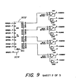
- Figure 9 is the logic diagram of PC HUX 305.
- 2:1 MUX's 901, 902, and 903 each handle four bits of the total 12 bit address.
- Two twelve-bit addresses are presented as the inputs: PCPADOO through PCPADIO and PCRll from PC 301 and PC +1 adder 303; and BRPADOO through BRPAD10 and BiLll from branch latch 314 and branch +1 adder 304.
- Note that the inverse states of the PCPAD and BRPAD signals are input to the 2:1 MUX's, but the non-inverse states of PCR11 and BRLII are input (pins A3 and B3 of 2:1 HUX 903); this accomplishes the toggling of the least significant bit mentioned above in connection with incrementing by one.
- One of the two twelve-bit addresses is selected depending on the conditions previously discussed, and is output as the twelve-bit address PCADDROO through PCADDRll to MUX 306 ( Figure 11), and as the twelve-bit address PCADROO through PCADRII to PC 301 ( Figure 8).
- Figure 10 depicts the logic diagram of branch address forwarding circuit 313. It receives the twelve-bit branch address BRADROO through BRADR11 from branch HUX 302 ( Figures 5 and 6), and generates, by conventional gating means, the twelve bit branch address BRADDROO through BRADDRII to MUX 306 ( Figure 11), and the twelve-bit branch address BRADOO through BRAD11 to branch latch 314 ( Figure 7).
- the output address has the same value as the input address, but is established in the necessary timing relationships previously discussed.
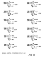
- Figure 11 depicts the logic diagram of MUX 306, constructed of three eight-bit 3916 buffer line drivers 1101, 1102, and 1103.. Each of these has the ability to function as a 2:1 MUX: a logic low on pin 1 causes the signals on pins 2, 4, 6, and 8 to be passed to output pins 18, 16, 14, and 12 respectively; a logic low on pin 19 causes input signals on pins 11, 13, 15, and 17 to pass to output pins 9, 7, 5, and 3 respectively. It is seen that the 24 output pins are connected together in 12 pairs. (For example, pin 18 of buffer line driver 1102 bears the signal name UADDR00, and pin 9 of buffer line driver 1103 bears the same signal name.
- Figure 12 is the logic diagram of control store 307, which comprises twenty-five 4K by 4 bit RAM chips, resulting in a 4K by 100 bit store.
- the twelve bit address UADDR00 through UADD811 is applied in parallel to each of the twenty-five chips which, assuming the CWRITEn aignals to be FALSE, each output four of the bits of the location specified by the address. (CWRITEn will be TRUE only when loading control store 307, not discussed herein.)
- the 100 output lines CS00 through CS99 comprise the 100 bit output of control store 307. Only the 96 bits CSOO through CS95 are presently used in the current embodiment.
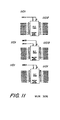
- FIGS 13 and 14 are the logic diagrams of prefetch register 308 and prefetch buffer 309 respectively, which together comprise the dual prefetch path of the present invention.
- Prefetch register 308 comprises a 96 bit register, packaged as 12 octal (i.e., eight circuits per package) flip-flop chips. It is loaded, as previously discussed, with the microinstruction that is to be executed next if the current microinstruction does not branch, the microinstruction appearing on the control store 307 outputs CS00 through CS95 at the end of the first 70 as of the 140 ns microinstruction cycle, as controlled by the signal LAST70CLKn coming TRUE.
- the 96 outputs SELUIROO through SELUIR95 are the inputs to microword register 310. If the current microinstruction is not to branch, the microinstruction from prefetch register 308 will thus be transferred to microword register 310 and become the next executing microinstruction.
- Prefetch buffer 309 comprises 12 octal buffer line drivers. Note that these are not flip-flops, and thus the prefetch buffer 309 it not a regicter; (i.e., it does not store the control store 307 outputs, but only passes them on to microword register 310).
- prefetch buffer 309 passes the branch target microinstruction, appearing on the 96 control store 307 outputs CS00 through CS95 at the conclusion of the current microinstruction cycle through to the microword register 310 inputs on lines SELUIROO through SELUIR95. If the current microinstruction is to branch, it is through this path that the target microinstruction becomes the next executing microinstruction.
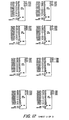
- Figure 15 is the logic diagram of microword register 310, comprising 25 4-bit shift register chips.
- the inputs are the 96 lines SELUIROO through SELUIR95, which as discussed above come from prefetch register 308 if the present microinstruction is not to branch, or through prefetch buffer 309 if the present microinstrucrtion is to branch.
- SELUIROO through SELUIR95 will be clocked into microword register 310 by the TRUE-transition of the signal UIRCLKn 1501.
- the outputs of microword register 310 directly control the processing elements of the microprocessor (the ALU 312); thus, the microinstruction that is loaded into microword register 310 becomes the executing microinstruction.
- Figure 16 shows detailed timings of the interactions between control store 307, prefetch register 308, prefetch buffer 309, and microword register 310 for the instruction sequence of Table 1.
- Line 1601 defines 3 consecutive microinstruction cycles, and line 1602 associates them with nanosecond timing. It is assumed that microinstruction 100 (from Table 1) is executed during cycle 1. Given that microinstruction 100 is a conditional branch to 400, which is assumed not to be taken, we now consider how microinstruction 101 (the next sequential microinstruction) is executed during cycle 2.
- microinstruction 100 was reached by being the next sequential instruction microinstruction to a previously executed microinstruction.
- its address (100) is at this time contained in PC 301. (Had it been reached as a branch target its address would be in branch latch 314, as previously discussed.)
- the address (100) of microinstruction 100 is incremented by one, to 101, through PC +1 adder 303, fed through PC MUX 305 and MUX 306 to control store 307.
- the microinstruction from location 101 is available at the control store outputs, as shown by line 1607.
- control store 307 is accessed with the branch address of target microinstruction 400, as obtained from currently executing microinstruction 100. As previously described, this is obtained through branch HUX 302 and MUX 306. Branch target microinstruction 400 is available at the CS outputs late in cycle 1, as line 1607 shows.
- microinstruction 101 occupies the microword register, and is the currently executing instruction, during cycle 2.
- the value "101,” is transferred from PC HUX 305 on signal lines PCADROO through PCADR11 into PC 301 for use in the fetches that will take place during cycle 2.
- microinstruction 101 includes a conditional branch to 200 that is to be taken, microinstruction 200 will occupy the microword register during cycle 3.
- control store location 102 the address being obtained by taking the value 101 from PC 301 and incrementing it to 102 in PC +1 adder 303
- location 102 the address being obtained by taking the value 101 from PC 301 and incrementing it to 102 in PC +1 adder 303
- microinstruction 102 is available at the control store outputs (line 1607) in time to be gated by LAST70CLK into the prefetch register (line 1608).
- the incremented address 102 is stored in PC 301.
- Control store location 200 (the target address obtained from microinstruction 101) is accessed during the aecond 70 ns of cycle 2 (line 1603), and branch target microinstruction 200 is available at the control store outputs and prefetch buffer inputs late in cycle 2 (line 1607).
- TESTPASSED inhibits gating next sequential microinstruction 102 from the prefetch register onto the SELUIR lines (line 1609); with reference to Figure 14, TESTPASSED enables gating branch target microinstruction 200 through the prefetch buffer onto the SELUIR lines.
- UIRCLK transits to TRUE (line 1605). Referring to Figure 15, this clocks branch target microinstruction 200 from the SELUIR lines into microword register 310. Thus, branch target microinstruction 200 is executed during cycle 3.
- microinstruction 201 is to be prefetched (line 1607). Since the currently executing microinstruction (200) was reached because it was a branch target, PC 301 will not come into play; the value 200 is stored in branch latch 314, and branch +1 adder 304 increments to the required address of 201.
- microinstruction 200 specifies 500 as its target address, and microinstruction 500 is prefetched. One of the two will be selected to execute during cycle 4, not discussed herein.
- Stack 1703 is a memory device with some number of memory locations, here four.
- Stack pointer 1701 is a flip flop register for containing the address of the location in stack 1703 which it is desired to access.
- Increment/decrement means 1705 can add or subtract by one the contents of stack pointer 1701. (Since stack locations are addressed in sequence, no provision is needed to load stack pointer 1701 with arbitrary contents, as would be the case for a random access memory.)
- Stack pointer 1701 must be able to contain as many values as there are locations in stack 1703. Since stack 1703 has four locations, the two bit positions of stack pointer 1701 can be incremented through the four combinations 00, 01, 10, and 11.
- Decoder 1702 comprises combinatorial gating to recognize each of the possible contents of stack pointer 1701 and enables the corresponding one of the four address selection lines 1706, which results in transferring data between the corresponding location of stack 1703 and bus 1704. (Operation of storage cevices is well known in the literature and will not be discussed herein.)
- Additional gating may be incorporated in decoder 1702 in order to detect "overflow” and "underflow".
- a stack is said to overflow when an attempt is made to exceed the capacity of the stack; it is said to underflow when an attempt is made to retrieve data from a stack when no data has previously been stored in it.
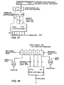
- Figure 18 presents an overview of the stack addressing scheme of the present invention.
- Stack 315 contains four twelve-bit locations, each of which is enabled by one of the addreas selection lines 1802.
- Each of address selection lines 1802 is the output of a stage of stack pointer 316, which is not, as in the prior art, an increment/decrement register, but is a shift register.
- Stack pointer 316 must contain at least aa many stages aa there are locations in stack 315. (In the present embodiment, the number of stages in stack pointer 316 ia two greater than the number of locations in stack 315.
- Stack pointer 316 is initially loaded with one 1 bit in its rightmost stage (stage 5) and is filled out with 0 bits. The 1 bit is shifted left after each stack write, and shifted right after each stack read. The stage containing the 1 bit at a given time has its output in the TRUE state; since the output lines of stack pointer 316 are in fact the address selection lines 1802, the correct address selection line is TRUE without the necessity for any of the gating or decoding which the prior art schemes require. Since many applications require stacks to operate quickly, it is an advantage that the delays associated with gating are eliminated. While the shifting of the bit is left to right as described above, this can be reversed and still result in utilizing the invention described herein.
- microinstruction 700 is a call microinstruction that invokes a subroutine
- the address 701 (derived, as previously discussed, by incrementing the 700 in PC +1 adder 303, passing it through PC MUX 305 onto the PCADROO through PCADR11 lines and loading it into PC 301) is output from PC 301 and stored on the top of the stack.
- the subroutine executes a return microinstruction
- the address 701 is retrieved from the top of the stack and input to branch MUX 302 as the next microinstruction address. Execution thus returns to the microinstruction following the call microinstruction.
- the contents of PC 301 are written to the next available stack location every microinstruction cycle.
- stack pointer 316 is shifted to the left only if the current microinstruction is a conditional call microinstruction and if the specified conditions are met. Therefore, only the PC 301 contents which are in fact the return addresses of call microinstructions that cause branching are retained in the stack-- for all other microinstructions, failing to shift stack pointer 316 results in keeping the same stack 315 location selected, and it will the contents will be overwritten during the next microinstruction cycle.
- stack pointer 316 is initially set to all zero bits except for a 1 bit in stage 5.
- the 1 bit in stage 5 selects location 3.
- location 3 is written into on a call microinstruction, the stack pointer 316 is shifted one stage to the left after writing so that the I bit is in stage 4, selecting location 2.
- Three more call microinstructions would result in filling locations 2, 1, and 0, shifting the one bit to stages 3, 2, and 1 respectively, at which point the stack would be full.
- Another attempt to store a return address in stack 315 shifts the one bit to stage 0.
- Nothing is actually written to the stack, there being no stack location associated with stage 1 of stack pointer 316. This constitutes overflow, but the present embodiment does not detect overflow until an attempt is made to retrieve the data that could not be written.
- the next attempt to read from stack 315 (an attempt to read back the data that could not be vritten) produces the OVERFLOW signal from gate 1803.
- Figure 19 shows the logic diagram of stack pointer 316. It comprises six D flip-flops.
- a D flip-flop captures and stores the state of the D (data) input at the time the CLK input transits to a logic high.
- Stage 0 is depicted at the top (element 1903) (conventionally called the “left") and stage 5 (associated with the first location in stack 315) at the bottom (element 1904) (conventionally called the "right”).
- Gating group 1901 is enabled by the BR TYP bits of the currently executing microinstruction being equal to 01, specifying a conditional call microinstruction, and by the TSTCNDO signal indicating that the requisite conditions are met, to produce the C STKC signal, indicating that a call microinstruction is to be performed.
- BR TYP bits being equal to 11 and TSTCNDO produce signal R STKC from gating group 1902 indicating that a return microinstruction is to be performed.
- C STKC shifts stack pointer 316 to lover numbered stages (by convention, "to the left"), denoting subsequent stack locations.
- gate 1905 is enabled by C STKC and STKC3 (the state of stage 3) and gates that state into stage 2.
- R STKC shifts stack pointer 316 to higher numbered stages ("to the right").
- Cate 1906 shifts the state of state 2 into stage 3.
- STKC2, STKC3, STKC4, and STKCS are passed through 2:1 MUX 1907, enabled by the RESTORE signal, onto STKW 0, STCW 1, STKW 2, and STKW 3 respectively, which are address selection lines 1802.
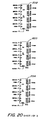
- Each of the four locations is constructed of six dual D flip-flops.
- a dual D flip-flop combines two D flip-flops in a package.
- element 2011 stores bits 0 and 1 of location 0, pins 1 and 3 being the inputs for bits 0 and 1 respectively, and pins 7 and 9 being the outputs for bits 0 and 1 respectively.
- Element 2011 requires STKW 0 of address select lines 1802 on pin 4, since it is part of location 0.
- Each of the four locations 2001, 2002, 2003, and 2004 is enabled by STKW 0, STKW 1, STKW 2, and STKW 3 respectively.
- Stack 315 is used to store the contents of PC 301, as discussed previously.
- the outputs of PC 301, namely PCROO through PCR11, are passed through 2:1 MUX's 2012, 2013, and 2014 under control of the RESTORE signal onto the STKIOO through STKI11 lines, which are input in parallel to each of the four stack locations; they are stored in the one location currently enabled by address selection lines 1802, as described above.
- PC 301 contents of PC 301 are stored in stack 315 every microinstruction cycle; however, stack pointer 316 is not shifted left except when call microinstructions are executed, as described above. Therefore, information written into stack 315 is not saved except for call microinstructions; if stack pointer 316 is not shifted, data written into a stack location during a microinstruction cycle will be overwritten the next microinstruction cycle.
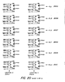
- Figure 21 depicts logic circuits for generating signals required by branch MUX 302 and branch address forwarding circuit 313 to for implementing return microinstructions.
- Gates 2101, 2102, 2103, and 2104 are enabled by the BR TYP bits of the currently executing microinstruction being equal to 11, denoting a return microinstruction.
- Each is enabled by one of the stages of shift register 316, denoting a location in stack 315 as previously discussed.
- gate 2103 is enabled by STKC3, meaning that stack location location 1 is presently selected to be written into. This in turn means that stack location 2 is the last stack location with a return address stored in it. Gate 2103 therefore produces the signal STK2 BR, denoting that the address contained in stack location 2 is now to be used as a branch target address.
- Branching to the location whose address is contained in stack location 2 is initiated by branch MUX 302 ( Figures 5 and 6).
- gate 502 is enabled by STK2 BR (just discusced) and passes STK 02, which reference to Figure 20 discloses to be bit 02 of stack location 2.
- Logic group 501 then outputs BRADR02.
- the other eleven logic groups depicted in Figures 5 and 6, together with group 501, output the 12-bit address BBADR00 through BRADRll, which results in branching to that address, as was previously discussed.
- Overflow is detected by gate 1803, shown in detail on Figure 21.
- BR TYP bits equal to 11, indicating a retura microinstruction, and STKC0, indicating a prior attempt to write beyond available locations in stack 315, as previously described, produce the signal STKOVFL denoting overflow.
Landscapes
- Engineering & Computer Science (AREA)
- Software Systems (AREA)
- Theoretical Computer Science (AREA)
- Physics & Mathematics (AREA)
- General Engineering & Computer Science (AREA)
- General Physics & Mathematics (AREA)
- Advance Control (AREA)
- Executing Machine-Instructions (AREA)
Applications Claiming Priority (2)
| Application Number | Priority Date | Filing Date | Title |
|---|---|---|---|
| US69559185A | 1985-01-28 | 1985-01-28 | |
| US695591 | 2003-10-28 |
Publications (2)
| Publication Number | Publication Date |
|---|---|
| EP0190484A2 true EP0190484A2 (fr) | 1986-08-13 |
| EP0190484A3 EP0190484A3 (fr) | 1988-09-21 |
Family
ID=24793645
Family Applications (1)
| Application Number | Title | Priority Date | Filing Date |
|---|---|---|---|
| EP85307894A Withdrawn EP0190484A3 (fr) | 1985-01-28 | 1985-10-31 | Ordinateur numérique à vitesse augmentée et méthode d'augmentation de vitesse |
Country Status (2)
| Country | Link |
|---|---|
| EP (1) | EP0190484A3 (fr) |
| JP (1) | JPS61221826A (fr) |
Cited By (4)
| Publication number | Priority date | Publication date | Assignee | Title |
|---|---|---|---|---|
| AU613232B2 (en) * | 1988-09-28 | 1991-07-25 | Data General Corporation | Wide branch instruction acceleration |
| EP0317119A3 (fr) * | 1987-11-05 | 1991-09-11 | Raytheon Company | Générateur de micro-instruction suivante, dans une unité de commande à micro-instructions |
| EP0322769A3 (fr) * | 1987-12-25 | 1992-05-20 | Hitachi, Ltd. | Dispositif de traitement de données adapté à un traitement de grande vitesse |
| EP1280052A3 (fr) * | 2001-07-27 | 2003-04-09 | STMicroelectronics, Inc. | Architecture d'extraction de branchement à pénalité de branchement réduit, sans prévision de branchement |
Family Cites Families (1)
| Publication number | Priority date | Publication date | Assignee | Title |
|---|---|---|---|---|
| DE3382250D1 (de) * | 1982-08-23 | 1991-05-16 | Western Electric Co | Mechanismus zur berechnung der naechsten adresse vor ihrer durchfuehrung. |
-
1985
- 1985-10-31 EP EP85307894A patent/EP0190484A3/fr not_active Withdrawn
-
1986
- 1986-01-28 JP JP1666986A patent/JPS61221826A/ja active Pending
Cited By (5)
| Publication number | Priority date | Publication date | Assignee | Title |
|---|---|---|---|---|
| EP0317119A3 (fr) * | 1987-11-05 | 1991-09-11 | Raytheon Company | Générateur de micro-instruction suivante, dans une unité de commande à micro-instructions |
| EP0322769A3 (fr) * | 1987-12-25 | 1992-05-20 | Hitachi, Ltd. | Dispositif de traitement de données adapté à un traitement de grande vitesse |
| AU613232B2 (en) * | 1988-09-28 | 1991-07-25 | Data General Corporation | Wide branch instruction acceleration |
| EP1280052A3 (fr) * | 2001-07-27 | 2003-04-09 | STMicroelectronics, Inc. | Architecture d'extraction de branchement à pénalité de branchement réduit, sans prévision de branchement |
| US7010675B2 (en) | 2001-07-27 | 2006-03-07 | Stmicroelectronics, Inc. | Fetch branch architecture for reducing branch penalty without branch prediction |
Also Published As
| Publication number | Publication date |
|---|---|
| EP0190484A3 (fr) | 1988-09-21 |
| JPS61221826A (ja) | 1986-10-02 |
Similar Documents
| Publication | Publication Date | Title |
|---|---|---|
| EP0114304B1 (fr) | Assistance matérielle et méthode de traitement de vecteur | |
| US4430706A (en) | Branch prediction apparatus and method for a data processing system | |
| EP0407911B1 (fr) | Dispositif et méthode de traitement en parallèle | |
| US5485587A (en) | Data processor calculating branch target address of a branch instruction in parallel with decoding of the instruction | |
| US4435756A (en) | Branch predicting computer | |
| EP0111407A2 (fr) | Unité de commande microprogrammée pour traiter des sous-routines microprgrammées et des interruptions dans l'occurence | |
| US5765007A (en) | Microinstruction sequencer having multiple control stores for loading different rank registers in parallel | |
| EP0592404B1 (fr) | Appareil et procede d'obtention d'une ante-memoire a blocage | |
| US4394729A (en) | Jump return stack | |
| US4884244A (en) | Method of addressing a computer memory | |
| EP0010196B1 (fr) | Circuit et procédé de contrôle pour mémoires digitales | |
| EP0223150B1 (fr) | Dispositif de traitement d'information | |
| EP0190484A2 (fr) | Ordinateur numérique à vitesse augmentée et méthode d'augmentation de vitesse | |
| US5526500A (en) | System for operand bypassing to allow a one and one-half cycle cache memory access time for sequential load and branch instructions | |
| US4870567A (en) | Microprogram control system | |
| US5363490A (en) | Apparatus for and method of conditionally aborting an instruction within a pipelined architecture | |
| EP0440908A2 (fr) | Technique de génération d'adresse pendant un cycle de décodage d'instruction dans un processeur RISC | |
| US4467410A (en) | Multi-phase subroutine control circuitry | |
| AU540728B2 (en) | Stack for a data processor | |
| EP0317119B1 (fr) | Générateur de micro-instruction suivante, dans une unité de commande à micro-instructions |
Legal Events
| Date | Code | Title | Description |
|---|---|---|---|
| PUAI | Public reference made under article 153(3) epc to a published international application that has entered the european phase |
Free format text: ORIGINAL CODE: 0009012 |
|
| AK | Designated contracting states |
Kind code of ref document: A2 Designated state(s): DE FR GB |
|
| PUAL | Search report despatched |
Free format text: ORIGINAL CODE: 0009013 |
|
| AK | Designated contracting states |
Kind code of ref document: A3 Designated state(s): DE FR GB |
|
| 17P | Request for examination filed |
Effective date: 19890220 |
|
| 17Q | First examination report despatched |
Effective date: 19901113 |
|
| STAA | Information on the status of an ep patent application or granted ep patent |
Free format text: STATUS: THE APPLICATION IS DEEMED TO BE WITHDRAWN |
|
| 18D | Application deemed to be withdrawn |
Effective date: 19910524 |
|
| RIN1 | Information on inventor provided before grant (corrected) |
Inventor name: NEALON, JAMES T. Inventor name: BREWER, TONY |