EP0191379A2 - Speicheranordnung des dynamischen Typs - Google Patents
Speicheranordnung des dynamischen Typs Download PDFInfo
- Publication number
- EP0191379A2 EP0191379A2 EP86101234A EP86101234A EP0191379A2 EP 0191379 A2 EP0191379 A2 EP 0191379A2 EP 86101234 A EP86101234 A EP 86101234A EP 86101234 A EP86101234 A EP 86101234A EP 0191379 A2 EP0191379 A2 EP 0191379A2
- Authority
- EP
- European Patent Office
- Prior art keywords
- blo
- bit lines
- capacitors
- memory device
- switching means
- Prior art date
- Legal status (The legal status is an assumption and is not a legal conclusion. Google has not performed a legal analysis and makes no representation as to the accuracy of the status listed.)
- Granted
Links
Images


Classifications
-
- G—PHYSICS
- G11—INFORMATION STORAGE
- G11C—STATIC STORES
- G11C11/00—Digital stores characterised by the use of particular electric or magnetic storage elements; Storage elements therefor
- G11C11/21—Digital stores characterised by the use of particular electric or magnetic storage elements; Storage elements therefor using electric elements
- G11C11/34—Digital stores characterised by the use of particular electric or magnetic storage elements; Storage elements therefor using electric elements using semiconductor devices
- G11C11/40—Digital stores characterised by the use of particular electric or magnetic storage elements; Storage elements therefor using electric elements using semiconductor devices using transistors
- G11C11/401—Digital stores characterised by the use of particular electric or magnetic storage elements; Storage elements therefor using electric elements using semiconductor devices using transistors forming cells needing refreshing or charge regeneration, i.e. dynamic cells
- G11C11/4063—Auxiliary circuits, e.g. for addressing, decoding, driving, writing, sensing or timing
- G11C11/407—Auxiliary circuits, e.g. for addressing, decoding, driving, writing, sensing or timing for memory cells of the field-effect type
- G11C11/409—Read-write [R-W] circuits
- G11C11/4099—Dummy cell treatment; Reference voltage generators
Definitions
- the present invention relates to a dynamic type memory device.
- a dynamic type memory device in which bit lines are precharged to 1/2 of a power source voltage VC in a precharge cycle is known.
- this memory device is constituted such that one end of each of paired bit lines BL and BL is connected to a sense amplifier 12, capacitor CS is connected to bit line BL through MOS transistor Ql whose gate is connected to word line WL, and capacitor CD is connected to bit line BL through MOS transistor Q whose gate is connected to dummy word line DWL.
- the other terminals of capacitors CS and CD are connected to fixed voltage terminal VA.
- bit lines BL and B L are connected to each other by MOS transistor Q 2 and are respectively connected through MOS transistors Q and Q 4 to a predetermined voltage line VCL which is kept at, for example, 1/2 VC.
- An equalizing signal ⁇ EQ is supplied to gates of MOS transistors Q 2 to Q 4 .
- Capacitors CS and CD are formed to have the same capacitance.
- MOS transistor Q 1 and capacitor CS constitute a memory cell 11.
- MOS transistor Q 5 and capacitor CD constitute a dummy cell 13.
- MOS transistors 0 2 to Q 4 when equalizing signal ⁇ EQ is at a high level, MOS transistors 0 2 to Q 4 are made conductive and both bit lines BL and BL are precharged to the level of 1/2 VC. After data is written into memory cell 11, the voltage of 1/2 VC is written into dummy cell 13. After a row address strobe signal RAS is set to a low level at time tl as shown in Fig. 2(A), when equalizing signal ⁇ EQ becomes low at time t 2 as shown in Fig. 2(C), MOS transistors 0 2 to Q are made non-conductive, so that bit lines BL and BL are isolated from each other.
- MOS transistors Q 2 to Q are made conductive and both potentials of bit lines BL and BL are set to 1/2 VC. After the voltage of the 1/2 VC level is written into dummy cell 13, the potential of dummy word line DWL is set low as shown in Fig. 2(D).
- a memory device shown in Fig. 3 is constituted similarly to that shown in Fig. 1 except that dummy cell 13 and MOS transistors Q and Q 4 are removed.
- This memory device operates in accordance with signal waveforms shown in Figs. 4A to 4D. Namely, in this memory device, after row address strobe signal RAS is set at a low level as shown in Fig. 4(A), equalizing signal 0 EQ is set at a high level as shown in Fig. 4(C). Thereafter, when the potential of word line WL is set at a high level as shown in Fig.
- the data in memory cell 11 is read out and outputted onto bit lines BL and BL and the potentials of bit lines BL and BL are changed in accordance with the data read out as shown in Fig. 4(D).
- Fig. 4(D) By equalizing the potentials of bit lines BL and BL in initial time of each readout operation as described above, data can be read out without being influenced due to the fluctuation of the power source voltage. However, data readout operation cannot be started until the potentials of bit lines BL and BL are equalized after strobe signal RAS is set at a low level, so that the access time eventually becomes long.
- a dynamic type memory device comprising: a plurality of memory cells each including one transistor and one capacitor; N first bit lines each of which is connected to the memory cells on the same column; N second bit lines; a plurality of word lines connected to the memory cells on the same row; a power source terminal and a reference potential terminal; a plurality of first capacitors each having a capacitance of 1/2 of that of each capacitor of the memory cells; a plurality of second capacitors each having a capacitance of 1/2 of that of each capacitor of the memory cells; and potential setting circuits for connecting the power source terminal to the second bit lines through the plurality of respective first capacitors and connecting the reference potential terminal to the second bit lines through the respective second capacitors in the data readout mode.
- the potential setting circuits for setting the potentials of the second bit lines through the first and second capacitors in a precharge cycle are used, so that it is not required to use any dummy word line. Therefore, there is no need to use any voltage step-up circuit and the structure of the memory device is simplified.
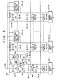
- Dummy cells or potential setting circuits PSC-1 to PSC-M are connected to bit lines BLO-1 to BLO-M in order to set the potentials of these bit lines.
- These potential setting circuits PSC-1 to PSC-M are constituted substantially in the same manner. A constitution of potential setting circuit PSC-1 will be described in detail.
- Potential setting circuit PSC-1 has capacitors C 1 and C 2 one end of which is connected to bit line BLO-1 and the other ends of which are respectively connected to power source terminal VC and a ground terminal V S through p- and n-channel MOS transistors Q 6 and Q 7 . Control signals CS and CS are supplied to gates of MOS transistors Q 6 and Q 7 , respectively.
- a connecting point of capacitor Cl and MOS transistor Q 6 is connected to constant voltage line VB through a dummy word line DWL 1 and a MOS transistor Q 8 .
- a connecting point of capacitor C 2 and MOS transistor Q 7 is connected to constant voltage line VB through a dummy word line DWL O and a MOS transistor Q 9 .
- a MOS transistor Q10 is connected between dummy word lines DWL 1 and DWL O . Equalizing signal ⁇ EQ is also supplied to gates of MOS transistors Q8 to Q10.
- MOS transistors Q2-1 to Q2-M, Q3-1 to Q3-M, and Q4-1 to Q4-M, and MOS transistors Q 8 to Q 10 of each of potential setting circuits PSC-1 to PSC-M are made conductive, thereby setting this memory device into the accessible state.
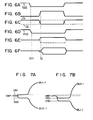
- word line WL 1 is set to a high level at time t2 as shown in Fig.
- MOS transistors Q 1 of memory cells MC-11 to MC-M1 are made conductive and the data in these memory cells are read out and outputted onto bit lines BL1-1 to BL1-M.
- MOS transistors Q 6 and Q 7 are conductive, the potentials of dummy word lines DWL 1 and DWL O are set to high and low levels as shown by solid and broken lines in Fig. 6E, respectively.
- Sense amplifiers SA-1 to SA-M amplify the difference between the potentials of bit lines BL1-1 to BL1-M and BLO-1 to BLO-M and set the potentials of these bit lines BL1-1 to BL1-M and BLO-1 to BLO-M as shown in Fig. 6F in accordance with the data read out from the memory cells.
- CB is a stray capacitance associated with each of bit lines BL1-1 and BLO-1.
- bit line BL1-1 changes from VBP to a potential level VB which is given by the following equation as shown in Fig. 7B.
- bit line BLO-1 changes from VBM to VBX which is obtained by the following equations.
- the data read out from the memory cell is independent of the precharge potentials of the pair of bit lines at a time just before the readout operation and the variation ranges of the signal level in the case where data "0" and "1" are read out can be made substantially equal.
- the potentials of the pair of bit lines can be equalized at a desired timing. In this case, since it takes a relatively long time for this equalizing operation, the bit lines can be precharged during this equalizing operation.
- potential setting circuit PSC-1 is constituted by CMOS transistors Q 6 and Q 7 , n-channel MOS transistors Q 8 to Q 10 , and capacitors C l and C 2' so that a large occupied area is unnecessary.
- control signals CS and CS change synchronously with the potential change of word lines WL selected, these control signals CS and CS can be easily formed in accordance with the change in potential of word lines WL.
- capacitor CS of the memory cell is connected to constant voltage terminal VA in the embodiment, in place of this constitution, it may also be connected to voltage source terminal VCP to which a fluctuating voltage varying in accordance with fluctuation of power source voltage VC is applied. With this constitution, the influence on the readout data due to the fluctuation of power source voltage VC can be suppressed.
Landscapes
- Engineering & Computer Science (AREA)
- Microelectronics & Electronic Packaging (AREA)
- Computer Hardware Design (AREA)
- Dram (AREA)
Applications Claiming Priority (2)
| Application Number | Priority Date | Filing Date | Title |
|---|---|---|---|
| JP18123/85 | 1985-02-01 | ||
| JP60018123A JPS61178795A (ja) | 1985-02-01 | 1985-02-01 | ダイナミツク型半導体記憶装置 |
Publications (3)
| Publication Number | Publication Date |
|---|---|
| EP0191379A2 true EP0191379A2 (de) | 1986-08-20 |
| EP0191379A3 EP0191379A3 (en) | 1989-01-25 |
| EP0191379B1 EP0191379B1 (de) | 1992-04-15 |
Family
ID=11962825
Family Applications (1)
| Application Number | Title | Priority Date | Filing Date |
|---|---|---|---|
| EP86101234A Expired EP0191379B1 (de) | 1985-02-01 | 1986-01-30 | Speicheranordnung des dynamischen Typs |
Country Status (4)
| Country | Link |
|---|---|
| US (1) | US4788668A (de) |
| EP (1) | EP0191379B1 (de) |
| JP (1) | JPS61178795A (de) |
| DE (1) | DE3684797D1 (de) |
Cited By (1)
| Publication number | Priority date | Publication date | Assignee | Title |
|---|---|---|---|---|
| EP0451453A1 (de) * | 1990-02-13 | 1991-10-16 | Nec Corporation | DRAM-Einrichtung mit Zweiweg-Spannungsversorgungssystem |
Families Citing this family (4)
| Publication number | Priority date | Publication date | Assignee | Title |
|---|---|---|---|---|
| US5528551A (en) * | 1987-05-21 | 1996-06-18 | Texas Instruments Inc | Read/write memory with plural memory cell write capability at a selected row address |
| FR2623653B1 (fr) * | 1987-11-24 | 1992-10-23 | Sgs Thomson Microelectronics | Procede de test de cellules de memoire electriquement programmable et circuit integre correspondant |
| JP2690506B2 (ja) * | 1988-06-07 | 1997-12-10 | 日本電気アイシーマイコンシステム株式会社 | 半導体記憶装置 |
| CN109995560A (zh) * | 2017-12-30 | 2019-07-09 | 中国移动通信集团贵州有限公司 | 云资源池管理系统及方法 |
Family Cites Families (11)
| Publication number | Priority date | Publication date | Assignee | Title |
|---|---|---|---|---|
| DE2647394C2 (de) * | 1976-10-20 | 1978-11-16 | Siemens Ag, 1000 Berlin Und 8000 Muenchen | MOS-Halbleiterspeicherbaustein |
| JPS5427734A (en) * | 1977-08-03 | 1979-03-02 | Toshiba Corp | Dynamic semiconductor memory |
| JPS5619585A (en) * | 1979-07-26 | 1981-02-24 | Toshiba Corp | Semiconductor memory unit |
| JPS5832789B2 (ja) * | 1980-07-18 | 1983-07-15 | 富士通株式会社 | 半導体メモリ |
| JPS57186291A (en) * | 1981-05-11 | 1982-11-16 | Mitsubishi Electric Corp | Semiconductor memory device |
| DE3280064D1 (de) * | 1981-06-29 | 1990-01-18 | Fujitsu Ltd | Dynamische direktzugriffspeicheranordnung. |
| US4420822A (en) * | 1982-03-19 | 1983-12-13 | Signetics Corporation | Field plate sensing in single transistor, single capacitor MOS random access memory |
| US4503523A (en) * | 1982-06-30 | 1985-03-05 | International Business Machines Corporation | Dynamic reference potential generating circuit arrangement |
| JPS59121691A (ja) * | 1982-12-01 | 1984-07-13 | Fujitsu Ltd | ダイナミツク型半導体記憶装置 |
| JPS59112490A (ja) * | 1982-12-17 | 1984-06-28 | Fujitsu Ltd | 半導体記憶装置 |
| US4547868A (en) * | 1984-07-26 | 1985-10-15 | Texas Instruments Incorporated | Dummy-cell circuitry for dynamic read/write memory |
-
1985
- 1985-02-01 JP JP60018123A patent/JPS61178795A/ja active Granted
-
1986
- 1986-01-30 DE DE8686101234T patent/DE3684797D1/de not_active Expired - Lifetime
- 1986-01-30 EP EP86101234A patent/EP0191379B1/de not_active Expired
- 1986-01-31 US US06/824,647 patent/US4788668A/en not_active Expired - Lifetime
Cited By (1)
| Publication number | Priority date | Publication date | Assignee | Title |
|---|---|---|---|---|
| EP0451453A1 (de) * | 1990-02-13 | 1991-10-16 | Nec Corporation | DRAM-Einrichtung mit Zweiweg-Spannungsversorgungssystem |
Also Published As
| Publication number | Publication date |
|---|---|
| EP0191379A3 (en) | 1989-01-25 |
| US4788668A (en) | 1988-11-29 |
| DE3684797D1 (de) | 1992-05-21 |
| JPH0510756B2 (de) | 1993-02-10 |
| EP0191379B1 (de) | 1992-04-15 |
| JPS61178795A (ja) | 1986-08-11 |
Similar Documents
| Publication | Publication Date | Title |
|---|---|---|
| US4947376A (en) | Charge-transfer sense amplifier for dram and operating method therefor | |
| US5051995A (en) | Semiconductor memory device having a test mode setting circuit | |
| US5274598A (en) | Semiconductor memory having improved sensing arrangement | |
| US6438049B1 (en) | Variable equilibrate voltage circuit for paired digit lines | |
| EP0077935B1 (de) | Dynamische Speicheranordnung | |
| US4748596A (en) | Semiconductor memory device with sense amplifiers | |
| US6728152B2 (en) | Sense amplifier for reduction of access device leakage | |
| US5255235A (en) | Dynamic random access memory with dummy word lines connected to bit line potential adjusting capacitors | |
| US5014241A (en) | Dynamic semiconductor memory device having reduced soft error rate | |
| EP0264929A2 (de) | Halbleiterspeicheranordnung mit verbesserter Bitzeilenordnung | |
| US4980862A (en) | Folded bitline dynamic ram with reduced shared supply voltages | |
| US5625588A (en) | Single-ended sensing using global bit lines for DRAM | |
| US5323345A (en) | Semiconductor memory device having read/write circuitry | |
| US4520466A (en) | Dynamic random access memory | |
| US5014246A (en) | Semiconductor memory device having shared sense amplifier and operating method thereof | |
| EP0073677B1 (de) | MIS Transistorschaltung mit einer Spannungshalteschaltung | |
| US4991142A (en) | Dynamic random access memory with improved sensing and refreshing | |
| US5959898A (en) | Dynamic cell plate sensing and equilibration in a memory device | |
| US5926410A (en) | Memory array architecture and method for dynamic cell plate sensing | |
| US4733373A (en) | Dynamic memory with improved arrangement for precharging bit lines | |
| US4788668A (en) | Dynamic type memory device including a reference potential generating circuit arrangement | |
| US4409672A (en) | Dynamic semiconductor memory device | |
| JP2980368B2 (ja) | ダイナミック型半導体記憶装置 | |
| US5894444A (en) | Cell plate referencing for dram sensing | |
| EP0318927A2 (de) | Halbleiterspeicher mit Abtastanordnung (ohne Funktionsstörung) |
Legal Events
| Date | Code | Title | Description |
|---|---|---|---|
| PUAI | Public reference made under article 153(3) epc to a published international application that has entered the european phase |
Free format text: ORIGINAL CODE: 0009012 |
|
| 17P | Request for examination filed |
Effective date: 19860130 |
|
| AK | Designated contracting states |
Kind code of ref document: A2 Designated state(s): DE FR GB |
|
| PUAL | Search report despatched |
Free format text: ORIGINAL CODE: 0009013 |
|
| AK | Designated contracting states |
Kind code of ref document: A3 Designated state(s): DE FR GB |
|
| 17Q | First examination report despatched |
Effective date: 19900814 |
|
| GRAA | (expected) grant |
Free format text: ORIGINAL CODE: 0009210 |
|
| AK | Designated contracting states |
Kind code of ref document: B1 Designated state(s): DE FR GB |
|
| REF | Corresponds to: |
Ref document number: 3684797 Country of ref document: DE Date of ref document: 19920521 |
|
| ET | Fr: translation filed | ||
| PLBE | No opposition filed within time limit |
Free format text: ORIGINAL CODE: 0009261 |
|
| STAA | Information on the status of an ep patent application or granted ep patent |
Free format text: STATUS: NO OPPOSITION FILED WITHIN TIME LIMIT |
|
| 26N | No opposition filed | ||
| REG | Reference to a national code |
Ref country code: GB Ref legal event code: 746 Effective date: 19981002 |
|
| REG | Reference to a national code |
Ref country code: FR Ref legal event code: D6 |
|
| REG | Reference to a national code |
Ref country code: GB Ref legal event code: IF02 |
|
| PGFP | Annual fee paid to national office [announced via postgrant information from national office to epo] |
Ref country code: FR Payment date: 20050110 Year of fee payment: 20 |
|
| PGFP | Annual fee paid to national office [announced via postgrant information from national office to epo] |
Ref country code: GB Payment date: 20050126 Year of fee payment: 20 |
|
| PGFP | Annual fee paid to national office [announced via postgrant information from national office to epo] |
Ref country code: DE Payment date: 20050127 Year of fee payment: 20 |
|
| REG | Reference to a national code |
Ref country code: GB Ref legal event code: PE20 |
|
| PG25 | Lapsed in a contracting state [announced via postgrant information from national office to epo] |
Ref country code: GB Free format text: LAPSE BECAUSE OF EXPIRATION OF PROTECTION Effective date: 20060129 |