EP0191596A2 - Verfahren und Vorrichtung zum Abtasten einer Flachschirm-Kathodenstrahlröhre - Google Patents
Verfahren und Vorrichtung zum Abtasten einer Flachschirm-Kathodenstrahlröhre Download PDFInfo
- Publication number
- EP0191596A2 EP0191596A2 EP86300777A EP86300777A EP0191596A2 EP 0191596 A2 EP0191596 A2 EP 0191596A2 EP 86300777 A EP86300777 A EP 86300777A EP 86300777 A EP86300777 A EP 86300777A EP 0191596 A2 EP0191596 A2 EP 0191596A2
- Authority
- EP
- European Patent Office
- Prior art keywords
- electrons
- scanning
- sheet
- field
- adjacent
- Prior art date
- Legal status (The legal status is an assumption and is not a legal conclusion. Google has not performed a legal analysis and makes no representation as to the accuracy of the status listed.)
- Withdrawn
Links
Images


Classifications
-
- H—ELECTRICITY
- H01—ELECTRIC ELEMENTS
- H01J—ELECTRIC DISCHARGE TUBES OR DISCHARGE LAMPS
- H01J31/00—Cathode ray tubes; Electron beam tubes
- H01J31/08—Cathode ray tubes; Electron beam tubes having a screen on or from which an image or pattern is formed, picked up, converted, or stored
- H01J31/10—Image or pattern display tubes, i.e. having electrical input and optical output; Flying-spot tubes for scanning purposes
- H01J31/12—Image or pattern display tubes, i.e. having electrical input and optical output; Flying-spot tubes for scanning purposes with luminescent screen
- H01J31/123—Flat display tubes
- H01J31/124—Flat display tubes using electron beam scanning
-
- H—ELECTRICITY
- H01—ELECTRIC ELEMENTS
- H01J—ELECTRIC DISCHARGE TUBES OR DISCHARGE LAMPS
- H01J29/00—Details of cathode-ray tubes or of electron-beam tubes of the types covered by group H01J31/00
- H01J29/46—Arrangements of electrodes and associated parts for generating or controlling the ray or beam, e.g. electron-optical arrangement
- H01J29/70—Arrangements for deflecting ray or beam
- H01J29/72—Arrangements for deflecting ray or beam along one straight line or along two perpendicular straight lines
- H01J29/74—Deflecting by electric fields only
-
- H—ELECTRICITY
- H01—ELECTRIC ELEMENTS
- H01J—ELECTRIC DISCHARGE TUBES OR DISCHARGE LAMPS
- H01J29/00—Details of cathode-ray tubes or of electron-beam tubes of the types covered by group H01J31/00
- H01J29/46—Arrangements of electrodes and associated parts for generating or controlling the ray or beam, e.g. electron-optical arrangement
- H01J29/70—Arrangements for deflecting ray or beam
- H01J29/72—Arrangements for deflecting ray or beam along one straight line or along two perpendicular straight lines
- H01J29/76—Deflecting by magnetic fields only
Definitions
- the invention relates to an apparatus and method for forming a scanning electron beam for a cathode ray tube device. More particularly, the invention relates to an apparatus and method for forming a scanning electron beam for a flat screen cathode ray tube device.
- a conventional cathode ray tube due to the geometry of scanning from an electron gun extending at right angles to the screen, results in a comparatively long neck extending away from the rear portion of the tube. Shortening the neck by moving the gun toward the screen complicates the compensation necessary to eliminate distortion and loss of focus due to the difference in distances between the gun and the center of the screen as compared to the extreme edges of the screen.
- the length of the neck of a conventional tube is a problem with a small portable set; however, if a truly large screen is desired, for example greater than 30 inches on the diagonal, the bulk of the picture tube resulting from the gun and neck structure becomes overwhelming.
- Cathode ray tube (“CRT") devices having flat screens are known in the prior art as well as the provision of elongated or line cathodes in such CRT devices.
- U.S. Patent Nos. 4,449,148, 4,451,846 and 4,451,852 each show a flat CRT screen and a plurality of line cathodes. Line cathodes are also shown in U.S. Patent Nos. 4,429,251, 4,435,672, 4,437,044 and 4,484,103.
- the line cathode of U.S. Patent No. 2,858,464 utilizes perforated grids, the holes of which define the number of electron beams which can be produced from the line cathode. Deflection coils taken with the perforated grids enable a scan of an electron beam to be formed along the length of the line cathode.
- a middle grid may include a long slit, rather than holes.
- emission control grids in conjunction with a slotted emission control plate form a scanning electron beam from the electrons emitted by a line cathode.
- Each adjacent channel continues the formation of a total line scan.
- the beam from the line cathode can be formed in accordance with U.S. Patent No. 2,858,464.
- the invention relates to a flat panel cathode ray tube ("CRT") display in which the scanning of one axis of the screen of the CRT device is accomplished by an analog addressing method.
- the method of analog addressing of the flat cathode ray tube simplifies electron beam formation and scanning by eliminating the requirement of complex scanning techniques and the constructions of prior art flat screen CRT displays.
- a narrow electron beam is formed from a line cathode by deflecting most of the emitted electrons.
- a sheet or layer of emitted electrons extends parallel to the plane of the flat screen.
- An analog horizontal-positioning deflection grid is adapted to deflect all portions of the sheet of electrons and prevents them from passing to the screen except for electrons emitted from an instantaneous single location along the horizontal axis of the ribbon cathode.
- the analog horizontal-positioning deflection grid controls emission from a single location by an analog nulling system.
- the horizontal-positioning deflection grid which is elongated, extends parallel to the ribbon cathode and the control grid and contains two deflection plates. The address and load plates are separated by a very narrow gap such that a slight deflection of the electron beam prevents the beam from passing between the plates.
- the load plate can be in the form of an elongated linear resistor.
- the address plate can be a substantially non-resistive elongated plate facing the load plate in order that any voltage applied to the address plate is established uniformly along its entire length.
- Horizontal scanning is accomplished by applying a varying control voltage to the address plate. If the control voltage is at any level between the highest and lowest voltage levels occurring at the ends of the resistive load plate, this voltage will be matched by an equal voltage at a single point along the length of the load plate. Since the voltages on the load and address plates are equal at one point along the horizontal axis of the plates, an electron beam emitted between the load plate and the address plate at that horizontal position cannot be deflected and thus will pass through the horizontal-positioning deflection grid.
- the voltages on the load plate and the address plate are unequal, causing the sheet of electrons passing through the gap between the plates to be deflected against one of the plates, thereby blocking or absorbing the entire sheet of electrons except for the narrow beam of electrons.
- This narrow beam exits the horizontal-positioning deflection grid and is accelerated by an elongated high voltage anode in an acceleration grid.
- the electron beam moves adjacent the viewing area of the display at a predetermined horizontal location.
- the beam is required to excite the phosphor on the viewing plate at the precise vertical location.
- the vertical deflection plates contain two parallel plates.
- the viewing plate is coated with a phosphor screen and has a transparent electrode on its inner surface.
- the back plate has a uniformly conductive electrode on its inner surface and is kept at a constant voltage.
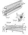
- the flat cathode ray tube (“CRT") of the invention as shown in FIG. 1 comprises a system 10 for forming a scanning electron beam 10a.
- the system comprises two vertical deflection plates which are a transparent viewing plate 11 and a back plate 12.
- a transparent substantially non-resistive electrode 13 On the inner surface of the viewing plate 11 is disposed a transparent substantially non-resistive electrode 13 in the form of a sheet.
- a suitable material for the transparent electrode 13 is a thin layer of tin oxide, which can readily be deposited on the surface of a plate.
- Electrode 13 which is transparent and substantially non-resistive is deposited in the form of a strip or sheet extending across plate 11.
- a phosphor coating 14 is applied to the inner surface of the transparent electrode 13 on the viewing plate 11.
- the phosphor coating 14 becomes perceptibly luminescent when impacted by and excited by an electron beam, as is well known by those skilled in the art of CRT devices.
- the transparent electrode 13 is connected to a first lead 15 which enables a variable voltage to be placed on the viewing plate 11.
- the back plate 12 is substantially parallel to the viewing plate 11 and has a conductive electrode 16 such as an electrode of metallic material deposited on the inner surface of back plate 12 in the form of a sheet.
- the metal electrode 16 which is substantially non-resistive is connected to a second lead 17 that enables a fixed voltage from a voltage source to be placed on . the back plate 12.
- the analog system 10 for forming a scanning electron beam 10a in FIGS. 1-4 forms the electron beam and also controls, focuses, deflects, and converges the electron beam.
- the system 10 additionally enables horizontal scanning of the electron beam by changing the horizontal position of the electron beam.
- the system 10 of the invention comprises a line or strip cathode 18, a control grid 19, an analog horizontal-positioning deflection grid 20, and an acceleration grid 21.
- the line cathode 18 which is disposed along a predetermined line is the source of electrons which are emitted in the form of a sheet of electrons extending at right angles to the predetermined line.
- the electrons then pass through the control grid 19 and an electron beam in the form of a horizontal sheet emerges.
- the control grid like the ribbon cathode 18, is elongated and extends parallel to the cathode.
- the control grid receives the intensity signal which can modulate the intensity of the electron beam. In the case of a television tube, the control grid can receive a video signals. In this way, the intensity with which the electron beam eventually impacts on the phosphor coating 14 of the viewing plate 11 can be controlled by using the control grid 19 to modulate the intensity of the electron beam.
- the electron beam in the form of a horizontal sheet then reaches the electrostatic analog horizontal-positioning deflection grid 20.
- Grid 20 which is elongated extends parallel to the ribbon cathode 18 and the control grid 19.
- the deflection grid 20 comprises an address plate 22 and a load plate 23.
- the load plate 23 of defection grid 20 comprises means for applying a referencing field to the sheet of emitted electrons which extends with respect to the plane of the sheet of electrons.
- the address plate 22 of deflection grid 20 comprises the means for generating a scanning field.
- the address and load plates are separated by a very narrow gap in order that slight deflection of electrons of the sheet passing through the gap will cause the deflected electrons of the sheet to be blocked or absorbed by the horizontal-positioning deflection grid 20.
- the elongated load plate 23 is in the form of an impedance element such as, for example, a linear resistor 23a which is connected by means of load leads 24 to a source of a constant voltage.
- the applying of a constant voltage at the ends of the load plate 23 creates a voltage gradient along the horizontal length of plate 23 as current passes through the linear resistance. A distinct voltage is thus present at each separate location along the horizontal length of load plate 23. (FIG. 5).
- the voltage gradient along the resistor 23a forms an electric field having a corresponding gradient.
- the address plate 22 extends parallel to the load plate 23 with a thin horizontal gap 25 between them through which only an undeflected electron beam can pass.
- the gap 25 is parallel to and is in alignment with the predetermined line along which line cathode 18 is disposed.
- the distinct voltages along the load plate 23 cause an electrostatic field to be exerted on any charged particles, i.e. electrons, passing through the horizontal gap 25 between the address plate 22 and the load plate 23.
- the address plate 22 is connected by means of address leads 26 to a varying scanning voltage.
- the address plate 22 is substantially non-resistive so that a voltage applied to address plate 22 exists uniformly along its horizontal length (FIG. 5).
- the varying scanning voltage when applied to the address plate 22 causes an electrostatic field to be exerted on charged particles in horizontal gap 25.
- the electrostatic fields generated by the address and load plates which interact across the gap are in opposite directions.
- the electrostatic field across the gap 25 created by the load plate 23 varies linearly while the force created by the address plate 22 is uniform.
- An electron passing through the horizontal gap 25 between the plates will be deflected by the resultant of the interacting electrostatic fields and will be blocked or absorbed by the analog horizontal-positioning deflection grid 20 at any points along the length of horizontal gap 25 where the interacting electrostatic fields from the plates do not cancel each other out (FIGS. 3 and 4).
- a voltage at some level between the highest and lowest voltage levels at the ends of the load plate 23 is selected and applied to the address plate 22 through address leads 26, there will always be one point along the length of horizontal gap 25 where the resultant electrostatic field exerted on the electron beam is zero (FIGS.
- the analog scanning system 10 of the invention can be used to form a scanning electron beam 10a by cutting off the emission of electrons by the ribbon cathode 18 except for a narrow electron beam at one horizontal location.
- the narrow beam at a single horizontal position emerging from the deflection grid 20 then passes through the horizontal slot 21a in acceleration grid 21 (FIGS. 1 and 2).
- the acceleration grid 21 is an elongated high voltage anode which is parallel to the ribbon cathode 18, control grid 19 and deflection grid 20. Grid 21 by virtue of the anode voltage applied thereto by terminal 21b accelerates the narrow electron beam 10a. If desired, the electron beam can then be passed through a focusing electrode (not shown) to enhance the focusing of beam 10a before entering the region between the viewing plate 11 and back plate 12.
- the horizontally-positioned narrow electron beam After emerging from the analog scanning system 10, the horizontally-positioned narrow electron beam enters the region between the viewing plate 11 and back plate 12 where the beam is electrostatically deflected to achieve vertical scanning of the screen.
- the level of the electrostatic field across plate 11 and plate 12 controls the curvilinear path of beam 10a as shown in FIGS. 2 and 6 and thereby the position of the horizontal scan lines of the raster on plate 11.
- the vertical deflection plates 11 and 12 described previously have voltages applied to them.
- a fixed voltage is applied to the metal electrode 16 on back plate 12 by means of lead 17.
- a variable voltage is applied to the transparent electrode 13 on viewing plate 11 by lead 15.
- Different voltages on the viewing plate 11 and back plate 12 create an electric field which electrostatically deflects the path of the electron beam.
- Progressively varying the voltage difference between the vertical deflection plates by progressively changing the voltage on transparent electrode 13, causes change of the position of the scan lines 40 (FIG. 1) upon which the electron beam impacts and excites the phosphor coating 14 on viewing plate 11.
- a progressively changing voltage i.e. a scanning voltage, causes the beam to move vertically along the viewing plate 11 in the form of a vertical scan.
- sawtooth or triangular voltage waveforms to the address plate 22 and the transparent electrode 13, the entire area of the viewing plate 11 can be raster scanned by a narrow electron beam.
- an array of analog scanning systems 10 is used, each having a separate line or ribbon cathode 18.
- the viewing plate 11 has deposited on its inner surface a series of horizontal lines 27 of different phosphor each of which are adapted to generate a different primary color when excited by electron beam 10a.
- the phosphors are typically selected to emit forms of red, green and blue light.
- the spacing between each colored line, as well as between each line of the scan are selected to be close enough to enable the instantaneous scanned portion of three adjacent lines to combine into a color image of proper fidelity and resolution.
- the electron beams emerging from each analog scanning system are conditioned to control generation of a single different color in achieving a proper color image. Therefore, the electron beam of each system is conditioned to intersect the lines of phosphor 27 capable of emitting the corresponding color. This is accomplished by staggering the positions of the scanning system 10 with respect to the distance to the screen. As a result, the electrostatic force across the vertical deflection plates causes each beam to impact upon the viewing plate 11 at a slightly different vertical position or scan line corresponding to the spacing between adjacent colored lines on the colored phosphor 27.
- the system of the invention for forming a scanning electron beam can also employ electromagnetic deflection as shown in FIGS. 7, 9 and 9.
- the analog scanning electromagnetic system 28 is similar in appearance and function to the electrostatic electron system 10 except for the configuration of the electromagnetic analog horizontal-positioning deflection grid 29.
- the deflection grid 29 comprises a load coil 30 and an address coil 31.
- An electron beam cannot pass through the horizontal slot 21a in the acceleration grid 21 if it has been deflected by an electromagnetic force.
- the address coil 31 is elongated and uniformly wound, e.g. in helical form, about the longitudinal axis thereof.
- the address coil is adapted to have a variable voltage applied thereto which produces a varying electromagnetic field.
- the load coil 30 is elongated but is not uniformly wound.
- the load coil can be in the form of a spiral extended in a conical form as shown in FIGS. 7 and 9.
- Either the number of turns of wire along the coil form or the size of the coil can vary along its horizontal length in order to create a magnetic field gradient which varies, e.g. linearly, between the ends of the load coil when a fixed voltage is applied to it.
- the uniform magnetic field from the address coil 31 and the linearly varying magnetic field from the load coil 30 oppose each other in the region between the two coils through which the horizontal sheet of electrons is emitted.
- the electron beam passing through the region where the resultant magnetic field is zero is not subject to any deflecting force and will pass through the slot in the acceleration grid 21.
- the remainder of the electrons in the sheet of electrons are subjected to a magnetic field having lines of flux extending in a horizontal direction, i.e. in the direction substantially of the longitudinal axis of the coils, which will deflect the electrons to the right or left as shown in FIG. 9, thereby blocking these, electrons from moving toward the screen.
- a narrow beam of electrons exists at a selected horizontal position, and by varying the voltage on the address coil 31, horizontal scanning of the viewing plate 11 can be achieved, similarly as described above for the case of electrostatic deflection.
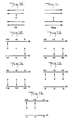
- FIGS. 10 and 11 show the upward and downward movement respectively of an electron moving out of the paper and with respect to the fields of coils 30 and 31, the direction of the fields being shown by arrows.
- FIGS. 12-16 show the movement of electrons in an electrostatic field between plates 22 and 23, the electrons being shown as moving toward the more positive voltage.
Landscapes
- Cathode-Ray Tubes And Fluorescent Screens For Display (AREA)
- Transforming Electric Information Into Light Information (AREA)
Applications Claiming Priority (2)
| Application Number | Priority Date | Filing Date | Title |
|---|---|---|---|
| US06/700,320 US4658188A (en) | 1985-02-11 | 1985-02-11 | Apparatus and method for scanning a flat screen cathode ray tube |
| US700320 | 1985-02-11 |
Publications (2)
| Publication Number | Publication Date |
|---|---|
| EP0191596A2 true EP0191596A2 (de) | 1986-08-20 |
| EP0191596A3 EP0191596A3 (de) | 1987-11-11 |
Family
ID=24813071
Family Applications (1)
| Application Number | Title | Priority Date | Filing Date |
|---|---|---|---|
| EP86300777A Withdrawn EP0191596A3 (de) | 1985-02-11 | 1986-02-05 | Verfahren und Vorrichtung zum Abtasten einer Flachschirm-Kathodenstrahlröhre |
Country Status (4)
| Country | Link |
|---|---|
| US (1) | US4658188A (de) |
| EP (1) | EP0191596A3 (de) |
| JP (1) | JPS61234183A (de) |
| CA (1) | CA1258538A (de) |
Families Citing this family (7)
| Publication number | Priority date | Publication date | Assignee | Title |
|---|---|---|---|---|
| DE3541164A1 (de) * | 1985-11-21 | 1987-05-27 | Standard Elektrik Lorenz Ag | Flache bildwiedergabevorrichtung |
| GB2186162B (en) * | 1986-01-30 | 1989-11-01 | Philips Electronic Associated | Cathode ray tube display system |
| JPS6419653A (en) * | 1987-07-14 | 1989-01-23 | Futaba Denshi Kogyo Kk | Flat display device |
| DE3831940A1 (de) * | 1988-09-20 | 1990-04-05 | Siemens Ag | Elektronenstrahlerzeuger |
| US5130614A (en) * | 1990-08-08 | 1992-07-14 | Massachusetts Institute Of Technology | Ribbon beam cathode ray tube |
| JP3671429B2 (ja) * | 1994-02-22 | 2005-07-13 | ソニー株式会社 | 画像表示装置および画像表示駆動方法 |
| US7471804B2 (en) * | 2003-09-03 | 2008-12-30 | Monster Cable Products, Inc. | Flat panel monitor frame with integral speakers |
Family Cites Families (3)
| Publication number | Priority date | Publication date | Assignee | Title |
|---|---|---|---|---|
| GB1354681A (en) * | 1970-04-02 | 1974-06-05 | Sanders Associates Inc | Cathode ray tube apparatus |
| KR850000970B1 (ko) * | 1981-02-10 | 1985-07-02 | 야마시다 도시히꼬 | 화상표시 장치 |
| US4484103A (en) * | 1982-09-23 | 1984-11-20 | Rca Corporation | Color selection electron beam guide assembly for flat panel display devices |
-
1985
- 1985-02-11 US US06/700,320 patent/US4658188A/en not_active Expired - Fee Related
-
1986
- 1986-01-29 CA CA000500645A patent/CA1258538A/en not_active Expired
- 1986-02-05 EP EP86300777A patent/EP0191596A3/de not_active Withdrawn
- 1986-02-10 JP JP61027749A patent/JPS61234183A/ja active Pending
Also Published As
| Publication number | Publication date |
|---|---|
| JPS61234183A (ja) | 1986-10-18 |
| US4658188A (en) | 1987-04-14 |
| CA1258538A (en) | 1989-08-15 |
| EP0191596A3 (de) | 1987-11-11 |
Similar Documents
| Publication | Publication Date | Title |
|---|---|---|
| CA1051500A (en) | Electron gun having an extended field electrostatic focus lens | |
| US2858464A (en) | Cathode ray tube | |
| EP0614209A1 (de) | Flache Bildschirmanordnung | |
| US4658188A (en) | Apparatus and method for scanning a flat screen cathode ray tube | |
| US3890541A (en) | Cathode ray tube apparatus | |
| WO1985005491A1 (en) | Flat panel display utilizing linear array of field emission cathodes | |
| US5130614A (en) | Ribbon beam cathode ray tube | |
| US4598233A (en) | Color display tube and device having such a tube | |
| US4853601A (en) | Multiple beam electron discharge tube having bipotential acceleration and convergence electrode structure | |
| GB2304984A (en) | Electron source | |
| KR20020013854A (ko) | 공간 절약형 음극선관 | |
| US5189335A (en) | Method of controlling electron beams in an image display apparatus | |
| EP0281191A2 (de) | Flache Kathodenstrahlröhre | |
| US4927218A (en) | Flat display tube comprising an emission system for emitting a planar electron beam, a deflection system and a modulation system | |
| US4032815A (en) | Collimated beam electron gun system for shaped beam cathode ray tube | |
| EP0569946B1 (de) | Hochauflösende Elektronenkanone | |
| US2930930A (en) | Electronic device | |
| GB2129205A (en) | Colour display tube | |
| US4044282A (en) | Cathode-ray tube with variable energy of beam electrons | |
| GB2138627A (en) | Display apparatus | |
| EP0153784B1 (de) | Flache Kathodenstrahlröhre | |
| US4698555A (en) | Cathode ray tube display system | |
| US3281621A (en) | Display storage tube with solenoidal focus and simultaneous deflection of writing and flood beams | |
| CA1224239A (en) | Flat cathode ray tube | |
| KR20020013853A (ko) | 정전기적으로 증폭된 편향을 채용하는 공간 절약형 음극선관 |
Legal Events
| Date | Code | Title | Description |
|---|---|---|---|
| PUAI | Public reference made under article 153(3) epc to a published international application that has entered the european phase |
Free format text: ORIGINAL CODE: 0009012 |
|
| AK | Designated contracting states |
Kind code of ref document: A2 Designated state(s): DE FR GB IT NL |
|
| PUAL | Search report despatched |
Free format text: ORIGINAL CODE: 0009013 |
|
| AK | Designated contracting states |
Kind code of ref document: A3 Designated state(s): DE FR GB IT NL |
|
| 17P | Request for examination filed |
Effective date: 19880510 |
|
| RAP1 | Party data changed (applicant data changed or rights of an application transferred) |
Owner name: CONTROL INTERFACE CORPORATION |
|
| 17Q | First examination report despatched |
Effective date: 19890103 |
|
| STAA | Information on the status of an ep patent application or granted ep patent |
Free format text: STATUS: THE APPLICATION IS DEEMED TO BE WITHDRAWN |
|
| 18D | Application deemed to be withdrawn |
Effective date: 19900609 |
|
| RIN1 | Information on inventor provided before grant (corrected) |
Inventor name: BOHMER, WILLIAM |