EP0192294A1 - Appareil à faisceau d'électrons comportant un émetteur d'électrons semi-conducteur - Google Patents
Appareil à faisceau d'électrons comportant un émetteur d'électrons semi-conducteur Download PDFInfo
- Publication number
- EP0192294A1 EP0192294A1 EP86200176A EP86200176A EP0192294A1 EP 0192294 A1 EP0192294 A1 EP 0192294A1 EP 86200176 A EP86200176 A EP 86200176A EP 86200176 A EP86200176 A EP 86200176A EP 0192294 A1 EP0192294 A1 EP 0192294A1
- Authority
- EP
- European Patent Office
- Prior art keywords
- electron beam
- electron
- beam apparatus
- emissive surface
- emissive
- Prior art date
- Legal status (The legal status is an assumption and is not a legal conclusion. Google has not performed a legal analysis and makes no representation as to the accuracy of the status listed.)
- Withdrawn
Links
Images
Classifications
-
- H—ELECTRICITY
- H01—ELECTRIC ELEMENTS
- H01J—ELECTRIC DISCHARGE TUBES OR DISCHARGE LAMPS
- H01J37/00—Discharge tubes with provision for introducing objects or material to be exposed to the discharge, e.g. for the purpose of examination or processing thereof
- H01J37/02—Details
- H01J37/04—Arrangements of electrodes and associated parts for generating or controlling the discharge, e.g. electron-optical arrangement or ion-optical arrangement
- H01J37/06—Electron sources; Electron guns
-
- H—ELECTRICITY
- H01—ELECTRIC ELEMENTS
- H01J—ELECTRIC DISCHARGE TUBES OR DISCHARGE LAMPS
- H01J1/00—Details of electrodes, of magnetic control means, of screens, or of the mounting or spacing thereof, common to two or more basic types of discharge tubes or lamps
- H01J1/02—Main electrodes
- H01J1/30—Cold cathodes, e.g. field-emissive cathode
- H01J1/308—Semiconductor cathodes, e.g. cathodes with PN junction layers
-
- H—ELECTRICITY
- H01—ELECTRIC ELEMENTS
- H01J—ELECTRIC DISCHARGE TUBES OR DISCHARGE LAMPS
- H01J1/00—Details of electrodes, of magnetic control means, of screens, or of the mounting or spacing thereof, common to two or more basic types of discharge tubes or lamps
- H01J1/02—Main electrodes
- H01J1/30—Cold cathodes, e.g. field-emissive cathode
-
- H—ELECTRICITY
- H01—ELECTRIC ELEMENTS
- H01J—ELECTRIC DISCHARGE TUBES OR DISCHARGE LAMPS
- H01J37/00—Discharge tubes with provision for introducing objects or material to be exposed to the discharge, e.g. for the purpose of examination or processing thereof
- H01J37/02—Details
- H01J37/04—Arrangements of electrodes and associated parts for generating or controlling the discharge, e.g. electron-optical arrangement or ion-optical arrangement
- H01J37/06—Electron sources; Electron guns
- H01J37/073—Electron guns using field emission, photo emission, or secondary emission electron sources
Definitions
- the invention relates to an electron beam apparatus comprising, arranged inside an evacuatable housing, an electron source which corn- prises an electron emitter for generating an electron beam having a comparatively high emission current density and an electron-optical lens system.
- an electron source which is capable of supplying an electron beam having a high current density, sufficient stability and attractive properties in relation to the electron-optical system of the apparatus.
- Electron beam apparatus comprising a conventional thermal cathode or a cathode made of LaB 6 , such as described in US 3,631,290, supply an electron beam whose brightness is insufficient for many applications. Maximum current densities which can be achieved in this respect are, for example, approximately 5a/cm 2 or 30 A/cm 2 , respectively.
- the emissive surface of such electron source which is of relevance for the electron-optical system is too large in relation to the electron-optical properties of the apparatus, so that optimum beam formation, spot formation or imaging cannot be achieved.
- Electron beam apparatus comprising a field emission source as described in US 3,631,291 are capable of supplying electron beams having a comparatively high current density, but such a source has several drawbacks such as instability of emissive power,positioning and geometry of the emitter. Moreover, such sources are not suitable for the supply of the frequently desired large total beam currents. From an electron-optical point of view, the dimension of the cathode and hence of the in this case virtual object of such a source is too small to obtain sufficiently high current densities. This is mainly due to the necessarily limited geometry of the emitter. Moreover, the energy spread of the electrons in an electron beam produced by the described sources is comparativaly large so that chromatic errors which are inadmissibly large are liable to occur in the electron-optical image.
- an electron beam apparatus of the kind set forth is characterized in that the electron emitter comprises a semi- conductor element in which there is provided, parallel to an emissive surface, a p-n junction which is to be connected in the reverse direction and whose dimensions define surface dimensions of the emissive surface to electron optical properties of the apparatus, the current density and the current intensity of an electron beam to be emitted being optimized at the same time.
- an electron beam apparatus in accordance with the invention uses a cold cathode as the electron emitter, the known thermal problems are avoided in this apparatus.
- This electron emitter uses this electron emitter, electron beams having a sufficiently high current density and current intensity can be readily achieved and the dimensions of the emissive surface defined by the transverse dimensions of the p-n junction enable optimum beam and spot shaping and electron-optical imaging.
- the semi- conductor electron emitter is constructed so as to operate with a p-n junction which is connected in the reverse direction. Due to the use of a source comprising a p-n junction connected in the reverse direction, so-called hot electrons are emitted. This means that the electrons to be emitted nust overcome a potential gradient when they emerge from the emissive surface.
- a largest transverse dimension of a consecutive emissive surface is limited to a maximum of, for example approximately 10 um.
- semiconductor techniques for examples ion implantation, it is comparatively easy to realize a p-n junction having such a dimension.
- This offers major advantages for electron beam apparatus, because the dimension of the emissive surface is thus adapted to electron-optical requirements to be imposed as regards the electron-optical lens system of the apparatus.
- a non-rotationally symmetrical electron-optical lens For optimizing the images use may be made, if desired, of a non-rotationally symmetrical electron-optical lens.
- Such an elongate emissive surface is preferably rectangular but may also be, far example, substantially elliptical, for example for realizing a particularly narrow spot (see US 3,881,136).
- a rectangular emissive surface may notably form a square which may be attractive, for exanple for beam writers, because this allows for the formation of an electron beam having a rectangular cross-section and hence a similar shaped writing electron spot.
- transverse dimensions of a singular emissive surface are limited to a maximum of, for example 10 um, and usually preferably to a value of between, for example 0.5 um and 5 um.
- composite emissive surfaces such as a central emissive surface which is surrounded by an annular second surface or an array or a matrix of several surfaces.
- a sufficiently large distance is chosen between the sub-regions of a composite emmisive surface, the emission of each of these surfaces can be simply and independently controlled.
- the p-n junction in the electron emitter is preferably located at a depth of from approximately 0.01 um to 0.05 um below the emissive surface.
- the semiconductor element of a preferred embodiment consists of Si; very good results have been obtained by means of this material also as regards service life. Howver, it is alternatively possible to use, for example SiC, Si-SiO 2 combinations, GaAs or similar 3-5 combinations. Actually, the choice of the material is not relevant for the invention for as long as the requirements as regards a high current density together with emissive surface dimensions which are adapted to the apparatus are satisfied and a sufficiently long service life can be achieved.
- the semiconductor element is provided at the area of the emissive surface with a substantially monomolecular layer of an appropriate material such as Cs, Ba, AgO, PtO, MiO, CO 2 , C etc.; good results have been obtained notably with Cs and Ba.
- the method of manufacturing a semiconductor electron emitter makes it comparatively simple to construct the emitter as a matrix or an array of emissive elements, for exanple a series of 10 elements or an orthogonal matrix of 10 x 10 elements.
- Such a Multi-beam apparatus is excellently suitable, for example for the production of integrated circuits, notably those circuits where the electron beam writes directly in the semi- conductor material i.e. without intermediate masks.
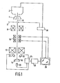
- a scanning electron microscope as shown in Figure 1 comprises an electron source 2, an anode 4, a control electrode 6, a condenser lens system 8, a beam scanning coil system 10, an objective lens system 12, and a specimen table 14.
- An electron beam 16 generated in the electron source is incident on a speciment 1'8 arranged on the specimen table.
- Detectors 20, 22 and 24 are capable of detecting different types of radiation as products of the interaction between the electron beam and the specimen.
- Via a signal selector 25 and a signal processing device 26 the signals are applied to a monitor 28.
- the monitor in a scanning electron microsoape is synchronized by signals from the beam scanning system and is also connected, for example to a control device 30 for beam blanking.
- a column of a scanning electron microscope in adapted form can serve, for example as a column for a beam writer as described, for example in US 3,491,236.
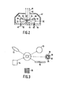
- An electron source as shown in Figure 2 comprises a semi- conductor element 40 which is accomodated in a housing 42 with a carrier table 44 and a diaphragm aperture 46 for the passage of the electron beam 16.
- the base plate comprises passages 48 for supply leads 50 for the electron emitter.
- the semiconductor element 40 contains a crystal semiconductor material 52 which consists, for exanple of Si, GaAs, SiC etc.
- a p-n junction 56 is provided in the crystal, transverse dimensions of said junction, that is to say the dimensions in its plane, being well defined.
- a part of the crystal is covered with, for example an oxide layer 58 on which there may be provided a conductive layer 60.
- the conductor 60 can act as a gate electrode.
- FIG 3 diagrammatically shows some preferred embodiments of emissive surfaces.
- the geometry of the emissive surface is in this case determined by the geometry of the p-n junction. All surfaces are chosen so that optimum adaptation to the electron-optical properties of the apparatus is obtained.
- a round emissive surface 70 has a diameter of, for exanple from approximately 0.5 to 5 um and thus has optimum dimensions as an object for further imaging in the apparatus. Due to this choice of the dimensions, the electrons which escape in the transverse direction, i.e. electrons which are not deliberately emitted, do not cause a disturbing field or disturbing heating of the semiconductor element at this area.
- a round emissive surface is suitable, for example for imaging apparatus such as an electron microscope.
- an emissive surface 72 For applications requiring an electron spot which is sharply defined mainly in one direction, use can be made of an emissive surface 72.
- the advantages of such a geometry are described in US 3,881,136; it can be used extremely well, for example for the formation of images in which a high resolution is desired mainly in one direction. The dimensions may then be, for example 1 x 5 ⁇ m 2 .
- a square emissive surface 74 with sides of, for example from 0.5 to 5 ⁇ m.
- Such a geometry is also very suitable for beam shaping as well as for splitting the electron spot into geometrically defined parts.
- the emissive surfaces 76 and 78 are composite emissive surfaces.
- the emissive surface 76 comprises a linear array of, for example 10 emissive sub-surfaces which are identical in this case.
- An apparatus can then operate with a nultiple beam as described in PHQ 82002 and PHQ 82006, it being possible to control each of the sub-beams individually.
- the sane consideration hold good for the emissive surface 78 in the form of a matrix of emissive sub-surfaces.
- Composite emissive surfaces are particularly suitable for electron beam writers, notably when such apparatus are used for the direct manufacture of integrated circuits,i.e. without the assistance of masks.
- a composite emissive surface 78 comprises a central sub-surface 80 and an annular sub-surface 82 as the emissive surfaces and a ring 84 as a non- emissive surface. Such a surface is useful, for example for measurement methods related to dark-field illumination etc. Such a composite surface may alternatively have a rectangular, square or other shape.
Landscapes
- Chemical & Material Sciences (AREA)
- Analytical Chemistry (AREA)
- Cold Cathode And The Manufacture (AREA)
- Electron Sources, Ion Sources (AREA)
- Cathode-Ray Tubes And Fluorescent Screens For Display (AREA)
- Photoreceptors In Electrophotography (AREA)
- Electron Beam Exposure (AREA)
Applications Claiming Priority (2)
| Application Number | Priority Date | Filing Date | Title |
|---|---|---|---|
| NL8500413 | 1985-02-14 | ||
| NL8500413A NL8500413A (nl) | 1985-02-14 | 1985-02-14 | Electronenbundelapparaat met een halfgeleider electronenemitter. |
Publications (1)
| Publication Number | Publication Date |
|---|---|
| EP0192294A1 true EP0192294A1 (fr) | 1986-08-27 |
Family
ID=19845521
Family Applications (1)
| Application Number | Title | Priority Date | Filing Date |
|---|---|---|---|
| EP86200176A Withdrawn EP0192294A1 (fr) | 1985-02-14 | 1986-02-10 | Appareil à faisceau d'électrons comportant un émetteur d'électrons semi-conducteur |
Country Status (7)
| Country | Link |
|---|---|
| US (1) | US4871911A (fr) |
| EP (1) | EP0192294A1 (fr) |
| JP (1) | JPS61193346A (fr) |
| KR (1) | KR860006823A (fr) |
| AU (1) | AU603762B2 (fr) |
| CA (1) | CA1254307A (fr) |
| NL (1) | NL8500413A (fr) |
Cited By (1)
| Publication number | Priority date | Publication date | Assignee | Title |
|---|---|---|---|---|
| EP0314216A1 (fr) * | 1987-10-29 | 1989-05-03 | Koninklijke Philips Electronics N.V. | Appareil à faisceau de particules chargées |
Families Citing this family (6)
| Publication number | Priority date | Publication date | Assignee | Title |
|---|---|---|---|---|
| GB2247345B (en) * | 1990-07-05 | 1995-04-05 | Haroon Ahmed | Integrated circuit structure analysis |
| JP3148353B2 (ja) * | 1991-05-30 | 2001-03-19 | ケーエルエー・インストルメンツ・コーポレーション | 電子ビーム検査方法とそのシステム |
| JP3730263B2 (ja) * | 1992-05-27 | 2005-12-21 | ケーエルエー・インストルメンツ・コーポレーション | 荷電粒子ビームを用いた自動基板検査の装置及び方法 |
| DE69419371T2 (de) * | 1993-09-02 | 1999-12-16 | Hamamatsu Photonics K.K., Hamamatsu | Photoemitter, Elektronenröhre, und Photodetektor |
| JP3101539B2 (ja) * | 1994-06-24 | 2000-10-23 | インターナショナル・ビジネス・マシーンズ・コーポレ−ション | 電子線ナノメトロジー・システム |
| US5586321A (en) * | 1995-02-21 | 1996-12-17 | Ramot Ltd. | Diffracting token router and applications thereof |
Citations (4)
| Publication number | Priority date | Publication date | Assignee | Title |
|---|---|---|---|---|
| EP0041119A1 (fr) * | 1980-06-02 | 1981-12-09 | International Business Machines Corporation | Dispositif d'émission d'électrons à froid |
| US4370797A (en) * | 1979-07-13 | 1983-02-01 | U.S. Philips Corporation | Method of semiconductor device for generating electron beams |
| GB2109159A (en) * | 1981-11-06 | 1983-05-25 | Philips Electronic Associated | Semiconductor electron source for display tubes and other equipment |
| DE3235064A1 (de) * | 1982-09-22 | 1984-03-22 | Siemens AG, 1000 Berlin und 8000 München | Tunnelkathodenmaske fuer die elektronenlithografie, verfahren zu ihrer herstellung und verfahren zu ihrem betrieb |
Family Cites Families (8)
| Publication number | Priority date | Publication date | Assignee | Title |
|---|---|---|---|---|
| BE549199A (fr) * | 1955-09-01 | |||
| US3334248A (en) * | 1965-02-02 | 1967-08-01 | Texas Instruments Inc | Space charge barrier hot electron cathode |
| GB1303660A (fr) * | 1969-11-12 | 1973-01-17 | ||
| US3631303A (en) * | 1970-01-19 | 1971-12-28 | Varian Associates | Iii-v cathodes having a built-in gradient of potential energy for increasing the emission efficiency |
| US3931519A (en) * | 1972-02-14 | 1976-01-06 | American Optical Corporation | Field emission electron gun |
| NL184549C (nl) * | 1978-01-27 | 1989-08-16 | Philips Nv | Halfgeleiderinrichting voor het opwekken van een elektronenstroom en weergeefinrichting voorzien van een dergelijke halfgeleiderinrichting. |
| JPS5698827A (en) * | 1979-01-04 | 1981-08-08 | Nippon Telegr & Teleph Corp <Ntt> | Electron beam exposure device |
| DE3538175C2 (de) * | 1984-11-21 | 1996-06-05 | Philips Electronics Nv | Halbleiteranordnung zum Erzeugen eines Elektronenstromes und ihre Verwendung |
-
1985
- 1985-02-14 NL NL8500413A patent/NL8500413A/nl not_active Application Discontinuation
- 1985-07-02 JP JP60144068A patent/JPS61193346A/ja active Pending
-
1986
- 1986-01-18 KR KR1019860000293A patent/KR860006823A/ko not_active Ceased
- 1986-02-10 EP EP86200176A patent/EP0192294A1/fr not_active Withdrawn
- 1986-02-11 AU AU53384/86A patent/AU603762B2/en not_active Ceased
- 1986-02-12 CA CA000501650A patent/CA1254307A/fr not_active Expired
-
1987
- 1987-07-17 US US07/077,060 patent/US4871911A/en not_active Expired - Lifetime
Patent Citations (4)
| Publication number | Priority date | Publication date | Assignee | Title |
|---|---|---|---|---|
| US4370797A (en) * | 1979-07-13 | 1983-02-01 | U.S. Philips Corporation | Method of semiconductor device for generating electron beams |
| EP0041119A1 (fr) * | 1980-06-02 | 1981-12-09 | International Business Machines Corporation | Dispositif d'émission d'électrons à froid |
| GB2109159A (en) * | 1981-11-06 | 1983-05-25 | Philips Electronic Associated | Semiconductor electron source for display tubes and other equipment |
| DE3235064A1 (de) * | 1982-09-22 | 1984-03-22 | Siemens AG, 1000 Berlin und 8000 München | Tunnelkathodenmaske fuer die elektronenlithografie, verfahren zu ihrer herstellung und verfahren zu ihrem betrieb |
Cited By (1)
| Publication number | Priority date | Publication date | Assignee | Title |
|---|---|---|---|---|
| EP0314216A1 (fr) * | 1987-10-29 | 1989-05-03 | Koninklijke Philips Electronics N.V. | Appareil à faisceau de particules chargées |
Also Published As
| Publication number | Publication date |
|---|---|
| KR860006823A (ko) | 1986-09-15 |
| NL8500413A (nl) | 1986-09-01 |
| AU603762B2 (en) | 1990-11-29 |
| CA1254307A (fr) | 1989-05-16 |
| AU5338486A (en) | 1986-08-21 |
| JPS61193346A (ja) | 1986-08-27 |
| US4871911A (en) | 1989-10-03 |
Similar Documents
| Publication | Publication Date | Title |
|---|---|---|
| US4682074A (en) | Electron-beam device and semiconductor device for use in such an electron-beam device | |
| US4303930A (en) | Semiconductor device for generating an electron beam and method of manufacturing same | |
| US4139773A (en) | Method and apparatus for producing bright high resolution ion beams | |
| US4528474A (en) | Method and apparatus for producing an electron beam from a thermionic cathode | |
| EP0992053B1 (fr) | Photocathode a grille destinee a l'emission controlee de faisceaux d'electrons simples et multiples | |
| US6943507B2 (en) | Device and method for controlling focussed electron beams | |
| US20030122085A1 (en) | Field ionization ion source | |
| US4871911A (en) | Electron beam apparatus comprising a semiconductor electron emitter | |
| NL8204240A (nl) | Halfgeleiderinrichting voor het emitteren van elektronen en inrichting voorzien van een dergelijke halfgeleiderinrichting. | |
| US5031200A (en) | Cathode for an X-ray tube and a tube including such a cathode | |
| US8450917B2 (en) | High-definition cathode ray tube and electron gun | |
| KR20020038696A (ko) | 컴팩트한 전계 방출 전자총 및 집속 렌즈 | |
| US4798957A (en) | Electron beam apparatus comprising an anode which is included in the cathode/Wehnelt unit | |
| JP2003513407A (ja) | 改良された熱電界放出の整列 | |
| EP0341781A1 (fr) | Appareil pour la formation d'un faisceau de particules chargées | |
| KR100201248B1 (ko) | 개선된 전계 방출 냉음극의 2차원 어레이를 갖는 전자총 | |
| JPS61131330A (ja) | 半導体装置 | |
| EP0314216A1 (fr) | Appareil à faisceau de particules chargées | |
| US5889359A (en) | Field-emission type cold cathode with enhanced electron beam axis symmetry | |
| JPH10223128A (ja) | 電子エミッタ | |
| EP0795193B1 (fr) | Dispositif optique a electrons presentant des zones emettrices allongees | |
| US6476544B1 (en) | Color cathode ray tube | |
| EP4639602A1 (fr) | Dispositif semi-conducteur de photocathode froide utilisant un champ électrique pour commander l'affinité électronique | |
| GB2322001A (en) | Electron emitters e.g. for displays | |
| Py et al. | In-plane refocusing of a microtips electron beam by a surrounding ring |
Legal Events
| Date | Code | Title | Description |
|---|---|---|---|
| PUAI | Public reference made under article 153(3) epc to a published international application that has entered the european phase |
Free format text: ORIGINAL CODE: 0009012 |
|
| AK | Designated contracting states |
Kind code of ref document: A1 Designated state(s): CH DE FR GB LI NL |
|
| 17P | Request for examination filed |
Effective date: 19870226 |
|
| 17Q | First examination report despatched |
Effective date: 19880629 |
|
| STAA | Information on the status of an ep patent application or granted ep patent |
Free format text: STATUS: THE APPLICATION IS DEEMED TO BE WITHDRAWN |
|
| 18D | Application deemed to be withdrawn |
Effective date: 19930901 |
|
| RIN1 | Information on inventor provided before grant (corrected) |
Inventor name: VAN DER MAST, KAREL DIEDERICK Inventor name: HOEBERECHTS, ARTHUR MARIE EUGENE Inventor name: TOLNER, HARM Inventor name: VAN GORKOM, GERARDUS GREGORIUS PETRUS |