EP0193211A2 - Circuit de délivrance d'impulsions d'amorçage - Google Patents
Circuit de délivrance d'impulsions d'amorçage Download PDFInfo
- Publication number
- EP0193211A2 EP0193211A2 EP86102680A EP86102680A EP0193211A2 EP 0193211 A2 EP0193211 A2 EP 0193211A2 EP 86102680 A EP86102680 A EP 86102680A EP 86102680 A EP86102680 A EP 86102680A EP 0193211 A2 EP0193211 A2 EP 0193211A2
- Authority
- EP
- European Patent Office
- Prior art keywords
- transistor
- circuit
- triac
- voltage
- emitter
- Prior art date
- Legal status (The legal status is an assumption and is not a legal conclusion. Google has not performed a legal analysis and makes no representation as to the accuracy of the status listed.)
- Granted
Links
Images

Classifications
-
- H—ELECTRICITY
- H03—ELECTRONIC CIRCUITRY
- H03K—PULSE TECHNIQUE
- H03K17/00—Electronic switching or gating, i.e. not by contact-making and –breaking
- H03K17/30—Modifications for providing a predetermined threshold before switching
- H03K17/305—Modifications for providing a predetermined threshold before switching in thyristor switches
Definitions
- the present invention relates to a circuit for delivering ignition pulses for a thyristor or triac according to the preamble of the main claim.
- a thyristor or triac which can also be represented by an equivalent circuit diagram which has two complementary transistors, the collector of one transistor being connected to the base of the other, the two emitters leading out these connections represent a two-pole circuit and the two collectors are connected to each other via a Zener diode.
- the emitter of one transistor is connected to an RC element, and that of the other is connected to the control electrode of the triac via a protective resistor.
- the present invention is therefore based on the object of varying the response threshold of this ignition pulse circuit and being able to influence the tilting via a special control input.
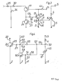
- the circuit according to FIG. 1 has a thyristor 1, which is connected with its one connection to ground 2 and with its other connection 3 via a load 4 to an AC voltage source 5.
- the load 4 could be a bare wire resistor of an electrical instantaneous water heater.
- the thyristor 1 has a control electrode 6, which is connected via a resistor 7 to an emitter 8 of an NPN transistor 9. This transistor 9 is part of a control circuit 10 for emitting the ignition pulses for the thyristor 1.
- the control circuit has a second transistor 11 which has a base 12 which is connected to a reference voltage source 14 via a line 13. A further line 15 branches off from line 13 and is connected to the collector 16 of transistor 9.
- the base 17 of the transistor 9 is connected via a line 18 to a branching point 19 which is connected on the one hand via a line 20 to the collector 21 of the transistor 11 and via a line 22 in parallel to a collector 23 of a third transistor 24, the base thereof 25 is connected via a line 26 to a terminal 27.
- a voltage source is then leased to the terminal 27 if the thyristor 1 is to be prevented from being ignited.
- the emitter 28 of the transistor 24 is connected to ground 2.
- the emitter 29 of the transistor 11 is connected via a diode 30 switched in the reverse direction to a further terminal 31 of the control circuit which is connected via a line 32 to a connection point 33 of an RC element, one branch of a capacitor 34 and the other branch consists of a resistor 35.
- the resistor 35 is led with a line 36 to a terminal 37, the branch point 33 is connected to ground 2 via the capacitor 34.
- the curve 40 is the line voltage, which is present, for example, at point 5, the curve 41 is the voltage curve at the branching point 33, reduced by the forward voltages of the diode 30 and the base-emitter diode of the transistor 11. Die am Point 14 applied reference voltage is represented by the value 42. This Eert is variable. At point 37, a DC voltage is applied, the value of which can be varied.
- the switch 38 is briefly closed each time the Metz voltage 40 passes through the envelope. Accordingly, the switch 38 opens, the voltage across the capacitor 34 increases measured the curve 43 until the capacitor voltage corresponds to the reference voltage 42.
- the transistors 11 and 9 are turned on, that is, an ignition pulse is given to the thyristor 1 via the resistor 7, since the circuit consisting of the two transistors 9 and 11 tilts, so that the voltage between the Emitters 29 and 8 collapse to almost zero.
- the lhyristor 1 becomes conductive and the load is fed during the current half-wave of the mains AC voltage, if it is positive. Negative half waves are suppressed. While the circuit 10 is also working during the negative half-wave, this does not affect the thyristor 1.
- the application of a voltage at terminal 27 causes transistor 24 to become conductive and thus to block transistor 9, even when the charging voltage of capacitor 34 has already reached the ignition voltage.
- the transistor 11 remains in the active region, so that the capacitor voltage is maintained until the transistor 24 is blocked again. With this the ignition takes place automatically. If it has not occurred during a mains half-wave, the capacitor is then discharged again by closing the switch 38.
- the advantage of this circuit is that, regardless of the position of the ignition angle, it always operates the flip-flop with the same voltage level. The level of the ignition voltage or the level of the ignition energy only depends on the level of the reference voltage at connection 14.
- the circuit is modified to the extent that a triac 45 is used instead of the thyristor 1.
- the circuit has been supplemented by a diode 46 which is connected in the course of a line 47 from ground 2 to a connection point 48, which is connected on the one hand to the emitter 8 of the transistor 9 and on the other hand to the resistor 7.
- a diode 49 is provided which is inserted into line 18. Diode 49 is forwardly connected to base 17, diode 46 is forwardly connected to point 48.
- the advantage of the circuit according to FIG. 3 is that mains half-waves of both polarities can be processed. However, the result of this is that the ignition electrode 6 can assume negative values with respect to ground 2.
- the two diodes 45 and 49 are provided. Diode 46 limits the occurrence of negative voltages at point 48 to the value of a forward voltage.
- the lead 18 is in the to the base 17 of this translator, the diode 49 turned on.
- the resistor 44 serves to limit the current flowing from the reference voltage source 14.
- the diode 30 serves to enable the capacitor 34 to be charged only via the resistor 35, even if the voltage of the reference voltage source 14 is higher than the permissible reverse voltage of the base-emitter diode of the transistor 11.
- the circuit according to FIG. 4 is intended to complement the circuit according to FIG. 3.
- a branching point 50 is provided between the load 4 and the triac 45, from which a line 51 leads, which leads to a second branching point 52. From this lead two lines 53 and 54, each provided with a resistor 55 and 56, to a further branching point 57, the line 53 leading directly there, the line 54, on the other hand, via the base collector path of a further transistor 58.
- the line 54 is otherwise connected to ground 2 via a resistor 59, and the emitter 60 of transistor 58 is likewise connected to ground 2.
- the point 57 is connected via a resistor 51 with a positive operating voltage 62 and the terminal 27 connected.
- the circuit according to FIG. 4 serves for undesired half-wave operation of the triac 45 with inductive load 4 and small ignition phase angles, for example when the load 4 is an asynchronous motor and the overall circuit serves as part of a speed control for this motor.
- the current lags behind the voltage, and it can happen that ignition pulses occur between the voltage zero crossing and the next current zero crossing.
- These ignition pulses remain ineffective since the triac switches off in the current zero passage and remains switched off for the rest of the half-wave. The next ignition therefore only takes place again in the following half-wave ", so that half-wave operation with undesirable direct current loading of the load results.
- the transistor 24 If the voltage at point 50 deviates significantly from zero at a level, regardless of whether in the positive or negative direction, the transistor 24 is blocked. This means that the triac can be ignited. Conversely, if the point 50 is at a voltage level very close to zero, the emission of ignition pulses is blocked due to the conduction of the transistor 24. This follows from the fact that when the voltage at point 50 increases in the positive direction, transistor 58 becomes conductive, which means that the voltage at point 57 becomes more negative. The transistor 24 is thus blocked. If the voltage at point 50 becomes negative, point 57 becomes equally negative. If the voltage falls below a threshold voltage at point 50, which depends on the values of the two resistors 55 and 61, transistor 24 also blocks again. The dimensioning of this circuit therefore depends crucially on the values of resistors 55 and 61 on the one hand and on those of resistors 56 and 59 on the other. furthermore, the level of the positive operating voltage 62 is of influence.
- the circuit shown in FIG. 4 blocks the occurrence of ignition pulses during the switch-on phases of the triac and thus ensures that ignition pulses are not triggered before the zero crossing of the previous current half-wave under inductive load.
- the flip-flop consisting of transistors 9 and 11 is switched off again when transistor 24 is switched on. The discharge process of the capacitor 34 is thus terminated after the ignition has taken place, so that only the current pulse required for the ignition is removed from the capacitor.
Landscapes
- Power Conversion In General (AREA)
- Ignition Installations For Internal Combustion Engines (AREA)
- Thyristor Switches And Gates (AREA)
- Electronic Switches (AREA)
Priority Applications (1)
| Application Number | Priority Date | Filing Date | Title |
|---|---|---|---|
| AT86102680T ATE62091T1 (de) | 1985-03-01 | 1986-03-01 | Schaltung zur abgabe von zuendimpulsen. |
Applications Claiming Priority (2)
| Application Number | Priority Date | Filing Date | Title |
|---|---|---|---|
| DE8506354 | 1985-03-01 | ||
| DE8506354U | 1985-03-01 |
Publications (3)
| Publication Number | Publication Date |
|---|---|
| EP0193211A2 true EP0193211A2 (fr) | 1986-09-03 |
| EP0193211A3 EP0193211A3 (en) | 1987-09-09 |
| EP0193211B1 EP0193211B1 (fr) | 1991-03-27 |
Family
ID=6778216
Family Applications (1)
| Application Number | Title | Priority Date | Filing Date |
|---|---|---|---|
| EP86102680A Expired - Lifetime EP0193211B1 (fr) | 1985-03-01 | 1986-03-01 | Circuit de délivrance d'impulsions d'amorçage |
Country Status (3)
| Country | Link |
|---|---|
| EP (1) | EP0193211B1 (fr) |
| AT (1) | ATE62091T1 (fr) |
| DE (1) | DE3678312D1 (fr) |
Family Cites Families (6)
| Publication number | Priority date | Publication date | Assignee | Title |
|---|---|---|---|---|
| FR1557188A (fr) * | 1967-03-13 | 1969-02-14 | ||
| CH534976A (de) * | 1970-09-17 | 1973-03-15 | Holzer Patent Ag | Nach dem Phasenanschnittprinzip arbeitende Schaltungsanordnung, zur Abgabe einer Zündspannung an einen Halbleiterschalter |
| DE2330969B2 (de) * | 1973-06-18 | 1976-01-02 | Nixdorf Computer Ag, 4790 Paderborn | Schaltungsanordnung zur Erzeugung eines definierten logischen Zustandes, insbesondere zur Überwachungssignalgabe in Datenverarbeitungsanlagen |
| AU5633273A (en) * | 1973-07-05 | 1974-12-05 | British Domestic Appliances | Thermal storage heaters thermal storage heaters |
| DE2405545B2 (de) * | 1974-02-06 | 1975-11-27 | Thielscher Electronic Gerhard Thielscher, 4100 Duisburg | Schaltungsanordnung zum zeitverzögerten Durchschalten einer Gleichspannung |
| FR2307507A1 (fr) * | 1975-04-18 | 1976-11-12 | Seb Sa | Dispositif de temporisation electronique pour grille-pain a ejection automatique |
-
1986
- 1986-03-01 EP EP86102680A patent/EP0193211B1/fr not_active Expired - Lifetime
- 1986-03-01 DE DE8686102680T patent/DE3678312D1/de not_active Expired - Lifetime
- 1986-03-01 AT AT86102680T patent/ATE62091T1/de not_active IP Right Cessation
Also Published As
| Publication number | Publication date |
|---|---|
| DE3678312D1 (de) | 1991-05-02 |
| EP0193211B1 (fr) | 1991-03-27 |
| ATE62091T1 (de) | 1991-04-15 |
| EP0193211A3 (en) | 1987-09-09 |
Similar Documents
| Publication | Publication Date | Title |
|---|---|---|
| DE2914313A1 (de) | Fehlerstrom-begrenzungsschaltung | |
| DE3213728A1 (de) | Motorstartschaltung | |
| DE3622293A1 (de) | Festkoerper-nebenschlussschaltkreis fuer leckstromleistungssteuerung | |
| DE2001580B2 (de) | Kurzschlußbeseitigungseinrichtung für Stromversorgungsschaltungen | |
| DE2343912C3 (de) | Stromversorgungseinrichtung, insbesondere für ein Kraftfahrzeug | |
| DE2504648A1 (de) | Einrichtung zum verhindern von ueberstrom oder ueberspannung | |
| DE3543573A1 (de) | Vorrichtung zur begrenzung des lichtbogen-entladestromes in einer gluehlampe | |
| EP0221574A2 (fr) | Circuit pour régulateur à courant alternatif à commande par impulsion | |
| EP0071945B1 (fr) | Circuit d'allumage pour thyristor de puissance | |
| DE2702142C3 (de) | Anordnung zur Steuerung der Drehzahl eines Universalmotors | |
| DE69400389T2 (de) | Steuerungssystem für einen elektrischen Umrichter | |
| EP0622902A2 (fr) | Relais semi-conducteur | |
| EP0193211B1 (fr) | Circuit de délivrance d'impulsions d'amorçage | |
| DE2251526A1 (de) | Steuerschaltung fuer kontaktlose schalter | |
| DE3606786A1 (de) | Schaltung zur abgabe von zuendimpulsen | |
| DE2023872A1 (de) | Elektrische Schalteinrichtung | |
| EP0141166A2 (fr) | Agencement de commutation pour outils électriques | |
| DE3149447A1 (de) | Regelungsschaltung zum konstanthalten der betriebsspannung eines elektrischen verbrauchers | |
| DE2738249C2 (de) | Anlaufstrombegrenzung für Universalmotor | |
| DE2827356C2 (fr) | ||
| DE2415630A1 (de) | Phasenanschnittssteuerschaltung aus einem triac und einem rc-glied | |
| DE1912903A1 (de) | Halbleiterschaltung zur Phasenanschnittssteuerung | |
| DE2111062A1 (de) | Schaltung zum Schalten eines Leistungsschalters | |
| DE3129111C1 (de) | Löscheinrichtung | |
| DE3707310A1 (de) | Thyristor-kommutierungsschaltung |
Legal Events
| Date | Code | Title | Description |
|---|---|---|---|
| PUAI | Public reference made under article 153(3) epc to a published international application that has entered the european phase |
Free format text: ORIGINAL CODE: 0009012 |
|
| AK | Designated contracting states |
Kind code of ref document: A2 Designated state(s): AT BE CH DE FR GB IT LI LU NL SE |
|
| PUAL | Search report despatched |
Free format text: ORIGINAL CODE: 0009013 |
|
| AK | Designated contracting states |
Kind code of ref document: A3 Designated state(s): AT BE CH DE FR GB IT LI LU NL SE |
|
| 17P | Request for examination filed |
Effective date: 19880421 |
|
| 17Q | First examination report despatched |
Effective date: 19891214 |
|
| RAP1 | Party data changed (applicant data changed or rights of an application transferred) |
Owner name: VAILLANT GMBH Owner name: SCHONEWELLE B.V. Owner name: VAILLANT LTD. Owner name: VAILLANT GES.M.B.H Owner name: VAILLANT S.A.R.L Owner name: N.V. VAILLANT S.A. Owner name: JOH. VAILLANT GMBH U. CO. |
|
| GRAA | (expected) grant |
Free format text: ORIGINAL CODE: 0009210 |
|
| AK | Designated contracting states |
Kind code of ref document: B1 Designated state(s): AT BE CH DE FR GB IT LI LU NL SE |
|
| REF | Corresponds to: |
Ref document number: 62091 Country of ref document: AT Date of ref document: 19910415 Kind code of ref document: T |
|
| ITF | It: translation for a ep patent filed | ||
| REF | Corresponds to: |
Ref document number: 3678312 Country of ref document: DE Date of ref document: 19910502 |
|
| GBT | Gb: translation of ep patent filed (gb section 77(6)(a)/1977) | ||
| ET | Fr: translation filed | ||
| PLBE | No opposition filed within time limit |
Free format text: ORIGINAL CODE: 0009261 |
|
| STAA | Information on the status of an ep patent application or granted ep patent |
Free format text: STATUS: NO OPPOSITION FILED WITHIN TIME LIMIT |
|
| 26N | No opposition filed | ||
| PGFP | Annual fee paid to national office [announced via postgrant information from national office to epo] |
Ref country code: SE Payment date: 19921207 Year of fee payment: 8 Ref country code: FR Payment date: 19921207 Year of fee payment: 8 |
|
| PGFP | Annual fee paid to national office [announced via postgrant information from national office to epo] |
Ref country code: LU Payment date: 19921209 Year of fee payment: 8 |
|
| PGFP | Annual fee paid to national office [announced via postgrant information from national office to epo] |
Ref country code: GB Payment date: 19921211 Year of fee payment: 8 |
|
| PGFP | Annual fee paid to national office [announced via postgrant information from national office to epo] |
Ref country code: BE Payment date: 19930208 Year of fee payment: 8 |
|
| EPTA | Lu: last paid annual fee | ||
| PGFP | Annual fee paid to national office [announced via postgrant information from national office to epo] |
Ref country code: NL Payment date: 19930331 Year of fee payment: 8 |
|
| NLT1 | Nl: modifications of names registered in virtue of documents presented to the patent office pursuant to art. 16 a, paragraph 1 |
Owner name: VAILLANT B.V. TE AMSTERDAM. |
|
| PG25 | Lapsed in a contracting state [announced via postgrant information from national office to epo] |
Ref country code: LU Free format text: LAPSE BECAUSE OF NON-PAYMENT OF DUE FEES Effective date: 19940301 Ref country code: GB Effective date: 19940301 |
|
| PG25 | Lapsed in a contracting state [announced via postgrant information from national office to epo] |
Ref country code: SE Free format text: LAPSE BECAUSE OF NON-PAYMENT OF DUE FEES Effective date: 19940302 |
|
| PG25 | Lapsed in a contracting state [announced via postgrant information from national office to epo] |
Ref country code: BE Effective date: 19940331 |
|
| BERE | Be: lapsed |
Owner name: S.A. VAILLANT N.V. Effective date: 19940331 |
|
| PG25 | Lapsed in a contracting state [announced via postgrant information from national office to epo] |
Ref country code: NL Effective date: 19941001 |
|
| GBPC | Gb: european patent ceased through non-payment of renewal fee |
Effective date: 19940301 |
|
| NLV4 | Nl: lapsed or anulled due to non-payment of the annual fee | ||
| PG25 | Lapsed in a contracting state [announced via postgrant information from national office to epo] |
Ref country code: FR Effective date: 19941130 |
|
| REG | Reference to a national code |
Ref country code: FR Ref legal event code: ST |
|
| EUG | Se: european patent has lapsed |
Ref document number: 86102680.5 Effective date: 19941010 |
|
| PGFP | Annual fee paid to national office [announced via postgrant information from national office to epo] |
Ref country code: AT Payment date: 19960229 Year of fee payment: 11 |
|
| PGFP | Annual fee paid to national office [announced via postgrant information from national office to epo] |
Ref country code: DE Payment date: 19960322 Year of fee payment: 11 |
|
| PGFP | Annual fee paid to national office [announced via postgrant information from national office to epo] |
Ref country code: CH Payment date: 19960328 Year of fee payment: 11 |
|
| PG25 | Lapsed in a contracting state [announced via postgrant information from national office to epo] |
Ref country code: AT Effective date: 19970301 |
|
| PG25 | Lapsed in a contracting state [announced via postgrant information from national office to epo] |
Ref country code: LI Effective date: 19970331 Ref country code: CH Effective date: 19970331 |
|
| REG | Reference to a national code |
Ref country code: CH Ref legal event code: PL |
|
| PG25 | Lapsed in a contracting state [announced via postgrant information from national office to epo] |
Ref country code: DE Effective date: 19971202 |
|
| PG25 | Lapsed in a contracting state [announced via postgrant information from national office to epo] |
Ref country code: IT Free format text: LAPSE BECAUSE OF NON-PAYMENT OF DUE FEES;WARNING: LAPSES OF ITALIAN PATENTS WITH EFFECTIVE DATE BEFORE 2007 MAY HAVE OCCURRED AT ANY TIME BEFORE 2007. THE CORRECT EFFECTIVE DATE MAY BE DIFFERENT FROM THE ONE RECORDED. Effective date: 20050301 |