EP0193273A2 - Synthétiseurs - Google Patents
Synthétiseurs Download PDFInfo
- Publication number
- EP0193273A2 EP0193273A2 EP86300512A EP86300512A EP0193273A2 EP 0193273 A2 EP0193273 A2 EP 0193273A2 EP 86300512 A EP86300512 A EP 86300512A EP 86300512 A EP86300512 A EP 86300512A EP 0193273 A2 EP0193273 A2 EP 0193273A2
- Authority
- EP
- European Patent Office
- Prior art keywords
- signal
- phase
- frequency
- subsidiary
- ripple
- Prior art date
- Legal status (The legal status is an assumption and is not a legal conclusion. Google has not performed a legal analysis and makes no representation as to the accuracy of the status listed.)
- Withdrawn
Links
Images

Classifications
-
- H—ELECTRICITY
- H03—ELECTRONIC CIRCUITRY
- H03L—AUTOMATIC CONTROL, STARTING, SYNCHRONISATION OR STABILISATION OF GENERATORS OF ELECTRONIC OSCILLATIONS OR PULSES
- H03L7/00—Automatic control of frequency or phase; Synchronisation
- H03L7/06—Automatic control of frequency or phase; Synchronisation using a reference signal applied to a frequency- or phase-locked loop
- H03L7/16—Indirect frequency synthesis, i.e. generating a desired one of a number of predetermined frequencies using a frequency- or phase-locked loop
- H03L7/18—Indirect frequency synthesis, i.e. generating a desired one of a number of predetermined frequencies using a frequency- or phase-locked loop using a frequency divider or counter in the loop
- H03L7/197—Indirect frequency synthesis, i.e. generating a desired one of a number of predetermined frequencies using a frequency- or phase-locked loop using a frequency divider or counter in the loop a time difference being used for locking the loop, the counter counting between numbers which are variable in time or the frequency divider dividing by a factor variable in time, e.g. for obtaining fractional frequency division
- H03L7/1974—Indirect frequency synthesis, i.e. generating a desired one of a number of predetermined frequencies using a frequency- or phase-locked loop using a frequency divider or counter in the loop a time difference being used for locking the loop, the counter counting between numbers which are variable in time or the frequency divider dividing by a factor variable in time, e.g. for obtaining fractional frequency division for fractional frequency division
- H03L7/1976—Indirect frequency synthesis, i.e. generating a desired one of a number of predetermined frequencies using a frequency- or phase-locked loop using a frequency divider or counter in the loop a time difference being used for locking the loop, the counter counting between numbers which are variable in time or the frequency divider dividing by a factor variable in time, e.g. for obtaining fractional frequency division for fractional frequency division using a phase accumulator for controlling the counter or frequency divider
-
- H—ELECTRICITY
- H03—ELECTRONIC CIRCUITRY
- H03L—AUTOMATIC CONTROL, STARTING, SYNCHRONISATION OR STABILISATION OF GENERATORS OF ELECTRONIC OSCILLATIONS OR PULSES
- H03L7/00—Automatic control of frequency or phase; Synchronisation
- H03L7/06—Automatic control of frequency or phase; Synchronisation using a reference signal applied to a frequency- or phase-locked loop
- H03L7/08—Details of the phase-locked loop
- H03L7/081—Details of the phase-locked loop provided with an additional controlled phase shifter
-
- H—ELECTRICITY
- H03—ELECTRONIC CIRCUITRY
- H03L—AUTOMATIC CONTROL, STARTING, SYNCHRONISATION OR STABILISATION OF GENERATORS OF ELECTRONIC OSCILLATIONS OR PULSES
- H03L7/00—Automatic control of frequency or phase; Synchronisation
- H03L7/06—Automatic control of frequency or phase; Synchronisation using a reference signal applied to a frequency- or phase-locked loop
- H03L7/16—Indirect frequency synthesis, i.e. generating a desired one of a number of predetermined frequencies using a frequency- or phase-locked loop
- H03L7/22—Indirect frequency synthesis, i.e. generating a desired one of a number of predetermined frequencies using a frequency- or phase-locked loop using more than one loop
- H03L7/23—Indirect frequency synthesis, i.e. generating a desired one of a number of predetermined frequencies using a frequency- or phase-locked loop using more than one loop with pulse counters or frequency dividers
Definitions
- the present invention relates to improvements in synthesisers of the fractional N type and in particular, to improvements for compensating the ripple signal produced in such synthesisers when operating in the fractional N mode.
- Frequency synthesisers usually comprise a voltage controlled oscillator (VCO) for providing an output signal and arranged in a phase lock loop.
- VCO voltage controlled oscillator
- the output signal of the VCO is fed via a variable divider to a phase detector which provides a control signal to the VCO in the presence of a phase difference between a reference signal from a reference source and the output signal from the divider.
- the output frequency of such synthesisers can, however, only be varied as a multiple of the reference signal frequency and it is usually desirable to vary the output frequency in relatively small increments. If the reference signal frequency is reduced in order to produce sufficiently small increments the settling time of the synthesiser may be increased to an extent such that it is impractical for many applications.
- fractional N synthesisers In a fractional N synthesiser the division ratio N of the variable divider is controlled in multiples of N such that, over a number of cycles of the reference signal, the mean value of the division ratio, termed N mean, is the desired fraction of the division ratio N.
- the operation of the synthesiser in the fractional N mode usually gives rise to a ripple signal on the output signal, which, in view of the phase lock loop configuration in the synthesiser, produces frequency modulation of the output signal from the voltage controlled oscillator and hence, the output signal has poor spectral purity.
- phase modulator between the variable divider and phase detector of the phase lock loop.
- the phase modulator is driven with a drive signal in order to provide compensation of the ripple signal.
- accurate compensation of the ripple signal is heavily dependent on the accurate setting of the level of the drive signal to the phase modulator.
- Previous attempts to use feedback control to correct the level of the drive signal, and thus to provide optimum compensation of the ripple signal have relied upon the extraction of a ripple rate signal from the control signal for the voltage controlled oscillator.
- the amplitude of the ripple signal is small compared to the amplitude of the control signal of the VCO and hence, it is difficult to control accurately the level of the drive signal for the phase modulator.
- a frequency synthesiser of the fractional N type comprising a primary voltage controlled oscillator for producing an output signal which is afforded to a phase detector via a primary divider to provide a control signal for the primary voltage controlled oscillator in the presence of a phase difference between a reference signal from a reference source and the signal afforded thereto from the primary divider, the division ratio of which may be varied in a fractional N mode to vary the frequency of the output signal in frequency steps smaller than the frequency of the reference signal and wherein a ripple signal tending thereby to be produced and causing frequency modulation of the output signal is compensated by a phase modulator, arranged to couple the primary divider and the phase detector and to receive a drive signal, wherein the synthesiser further comprises a subsidiary phase lock loop arranged to provide an enhanced representation of the ripple signal in dependence upon the signal afforded to the phase detector from the phase modulator, and a digital to analogue converter arranged to provide the drive signal for the phase modulator in dependence upon the enhanced representation
- the subsidiary phase lock loop comprises a subsidiary voltage controlled oscillator having a sensitivity lower than that of the primary voltage controlled oscillator, a subsidiary divider, and a subsidiary phase detector arranged to receive as a reference signal for the subsidiary phase lock loop a signal dependent upon the signal afforded to the phase detector from the phase modulator.
- the synthesiser may include a sense detecting circuit, responsive to the enhanced representation of the ripple signal, for providing a signal indicative of the sense of any error in the level of the drive signal to the phase modulator.
- the synthesiser may also include a voltage generator circuit arranged to provide a signal dependent upon the reciprocal of the mean division ratio of the primary divider, and wherein the digital to analogue converter comprises a multiplying digital to analogue converter arranged to receive a reference signal dependent upon the combination of the signal provided by the voltage generator circuit and the signal provided by the sense detecting circuit and wherein the digital to analogue converter is arranged to provide the drive signal for the phase modulator in dependence upon the reference signal afforded thereto.
- a voltage generator circuit arranged to provide a signal dependent upon the reciprocal of the mean division ratio of the primary divider
- the digital to analogue converter comprises a multiplying digital to analogue converter arranged to receive a reference signal dependent upon the combination of the signal provided by the voltage generator circuit and the signal provided by the sense detecting circuit and wherein the digital to analogue converter is arranged to provide the drive signal for the phase modulator in dependence upon the reference signal afforded thereto.
- a method of compensating a ripple signal tending to cause frequency modulation of the output signal in a fractional N type synthesiser of the type having, arranged in a phase lock loop, a phase detector for receiving a signal from a reference source and an output signal from a primary voltage controlled oscillator via a primary divider having a division ratio N which may be varied in a fractional N mode, and a phase modulator, arranged to couple the divider and the phase detector and for compensating the ripple signal in response to a drive signal fed thereto, the method comprising affording a signal to a subsidiary phase lock loop in dependence upon the signal afforded from the phase modulator to the phase detector thereby to provide an enhanced representation of the ripple signal, and providing via a digital to analogue converter the drive signal to the phase modulator in dependence upon the enhanced representation of the ripple signal.
- the method also comprises determining the sense of any error in the level of the drive signal to the phase modulator.
- the sense of any error in the level of the drive signal to the phase modulator is determined by affording the enhanced representation of the ripple signal provided by the subsidiary phase lock loop via a limiter to a first input of an exclusive OR gate and affording a signal dependent upon the output signal from the digital to analogue converter to a further input of the exclusive OR gate thereby to produce a signal at the output of the exclusive OR gate indicative of the sense of the error in the level of the drive signal to the phase modulator.
- the digital to analogue converter may be a multiplying digital to analogue converter having a reference signal input and the method further comprises providing a signal dependent upon the mean division ratio of the primary divider, and combining the signal dependent on this division ratio with a signal in dependence upon the enhanced representation of the ripple signal thereby to provide the input signal for the reference signal input of the multiplying digital to analogue converter.
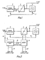
- the synthesiser 2 comprises a phase lock loop having a voltage controlled oscillator (VCO) 4 the output frequency of which F OUT is fed via a variable divider 6, having a division ration N, to a phase detector 8.
- the phase detector 8 also receives from a reference source (not shown), a reference signal having a reference frequency F ref and provides a control signal to the oscillator 4 along a loop 10 in the presence of a phase difference between the signals on its two inputs.
- the sense of the control signal from the phase detector 8 to the oscillator 4 is such that any phase difference between the input signals to the phase detector 8 is reduced to a minimum and hence any difference in the frequencies of these two input signals is reduced to zero.
- N mean a mean value of N, termed N mean, such that the output frequency
- the division ratio of the variable divider 6 is controlled by means of an arithmetic unit 12 and an adder 14.
- the arithmetic unit 12 is arranged to receive the reference frequency F ref along a line 16 and data indicative of the output frequency steps less than F ref along a data bus 18.
- the output of the arithmetic unit 12 is connected to the adder 14 by line 20 and the adder 14 is also arranged to receive data indicative of the output frequency steps greater than or equal to F ref along a data bus 22.
- the desired N/N + 1 pattern appropriate to generate the required N mean for a chosen output frequency may be obtained by an arithmetic unit having a BCD adder in combination with D-type flip-flops (not shown) for each decade of decimal N required.
- the data word fed to the arithmetic unit 12 is
- the first of these terms defines the capacity of the arithmetic unit 12 and the second term is the fractional offset, denoted by d.
- d fractional offset
- the required capacity of the aritmetic unit 12 is 1000 and three decades will be required.
- This type of system has the defect of poor spectral purity of the output signal because the continuously varying division ratio means that pulses from the variable divider 6 arrive at the input to the phase detector 8 at varying times to those arriving at the other input of the phase detector 8 from the reference source (not shown).
- the output of the phase detector 8 will therefore contain AC components, generally called a ripple signal, at frequencies related the offset of the output frequency F OUT from a whole multiple of the reference frequency Fref
- the ripple signal is fed around the loop and causes frequency modulation of the oscillator 4; producing poor spectral purity.
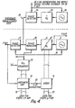
- Figure 3 illustrates a compensated fractional N sysnthesiser in which the spectral purity of the output signal F OUT may be improved.
- the data at the output of the D-type flip flops (not shown) in the arithmetic 12 represent the difference in phase which would exist between the input signals to the phase detector 8 if the output from the oscillator 4 were spectrally pure. Therefore the data at the output of the arithmetic unit 12 may be converted to analogue form by a digital to analogue (D/A) converter 24 and the analogue signal used to control a voltage controlled delay element, such as a phase modulator 26, at either input to the phase detector.
- D/A digital to analogue
- the phase detector does not perceive the phase perturbations caused by the ripple signal resulting from the variation in the division ratio of the variable divider 6. Hence, there is no spurious frequency modulation of the output signal from the oscillator 4.
- the level of the drive signal to the phase modulator 26 to give the delay required for cancellation can be determined as follows.
- a fractional N synthesiser has an output frequency of where the division ratio N is an integer and the fractional offset O ⁇ d ⁇ 1, and that the output signal F O UT is spectrally pure that is, the edges of the output signal from the variable divider 6 are regularly spaced.
- T ref is the period of the reference signal
- the period between the edges of the pulses in the reference signal and the edges of the pulses in the output of the variable divider 6 will vary. If at some time the edge of a reference signal pulse and the edge of a pulse of the output signal from the variable divider 6 coincide exactly, then the next variable divider output signal edge will precede the next reference signal edge by a time difference DT where
- This deviation between the reference signal Fref from the reference source and the output signal from the divider 6 increases such that the next respective edges will be separated by twice the amount of the first edges, the next by three times, and so on, until a division ratio of (N+l) is entered into the variable divider 6.
- the data at the output terminals of the flip flops used in the arithmetic unit 12 increases in the same pattern as the deviation betwen the inputs to the phase detector 8.
- the same pattern between these parameters means that the data at the output terminals of the flip flops may be used to compensate the ripple signal in the synthesiser. If the phase detector 8 is not to impose spurious frequency modulation on the output signal F OUT , either of its inputs may be delayed by an appropriate amount. However, freedom from spurious frequency modulation is dependent upon the accuracy of the compensation applied and it is difficult to obtain sideband levels below - 40 dB with respect to the output signal F OUT over a wide temperature range.
- the loop 10 usually includes a loop filter (not shown) but the low frequency perturbations caused by these conditions are not attenuated by the loop filter and are applied to the oscillator 4, thereby causing frequency modulation of the output signal F OUT .
- the synthesiser 2 is provided with the phase modulator 26 located between the variable divider 6 and the phase detector 8.
- the rate of the signal arriving at the phase detector 8 via the phase modulator 26 is constant and equal to the rate of the reference signal F ref .
- a subsidiary phase lock loop 28 is provided which comprises a subsidiary voltage controlled oscillator 30, a subsidiary divider 32 and a subsidiary phase detector 34.
- the subsidiary phase lock loop (PLL) 28 is arranged such that the output of the phase modulator 26 in the main loop is used to provide the reference signal for the subsidiary phase detector 34.
- a spurious FM deviation of DF Hz on the output signal F OUT caused by the ripple signal in the main loop, will cause a deviation of at the output of the subsidiary phase lock loop 28, where N 1 is the division ratio of the variable divider 6 in the main loop and N 2 is the division ratio of the subsidiary divider 32.
- This deviation in the subsidiary phase lock loop 28 will be associated with a variation of the tuning voltage of the subsidiary voltage controlled oscillator 30.
- This tuning voltage in the subsidiary phase lock loop 28 will have the same waveform as the ripple signal in the main loop and hence, can be used as a measure of the frequency modulation on the output signal F OUT of the oscillator 4.
- the subsidiary divider 32 has a fixed division ratio and hence, as the reference frequency for the subsidiary phase lock loop can only vary within a limited range, as determined by the ripple signal, the range of the output frequency of the subsidiary phase lock loop 28 is also limited. Therefore, the subsidiary voltage controlled oscillator 30 can be arranged to have a low sensitivity (Hz/volt) as it does not need a wide tuning range.
- the subsidiary phase lock loop 28 can provide an enhanced representation of the ripple signal causing frequency modulation of the output signal F OUT in dependence upon the signal afforded to the phase detector 8 from the phase modulator 26.
- the subsidiary voltage controlled oscillator 30 may comprise a voltage-tuned crystal oscillator (VCXO) as such oscillators have high stability and sufficiently low sensitivity, typically 100 Hz/volt at an output frequency of 10MHz.
- VCXO voltage-tuned crystal oscillator
- the 100pv peak ripple signal is now represented by a signal having a peak of 0.28V.
- the presence of a variation of the tuning voltage of the subsidiary voltage controlled oscillator 30 indicates that the oscillator 4 in the main loop is subject to frequency modulation but it does not indicate the sense in the error in the level of the drive signal to the phase modulator 26, that is whether the level of the drive signal to the phase modulator is causing over or under compensation of the ripple signal.
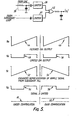
- the sense detecting circuit comprises a first limiter 36 arranged to receive the output signal from the D/A converter 24, shown in Figure 4, via a low pass filter 38, and a further limiter 40 for receiving a signal in dependence upon the enhanced representation of the ripple signal produced by the subsidiary phase lock loop 28.
- the outputs of the limiters 36 and 40 provide the inputs for an exclusive OR gate 42.
- the inclusion of the low pass filter 38 may be understood by considering a system with a reference frequency F ref of 100Khz and the output frequency F OUT Set to 45.6251M H z.
- the data word fed to the arithmetic unit 12 is 251 and hence, the required capacity of the arithmetic unit is 1000.
- the output of the D/A converter 24 contains two main frequency components - a 25 KHz component because the the accumulator in the arithmetic unit 12, having a capacity of 1000, overflows every four cycles of the 100 KHz reference frequency as 4 x 251 1000; and a 100 Hz component as 1000 cycles of the reference frequency are required to return the arithmetic unit 12 to its initial state.
- the 25KHz component is not particularly troublesome to the spectral purity of the output signal F OUT but can interfere with the operation of the limiter 36 and the exclusive OR gate 42 in the sense detecting circuit and is, therefore, removed by means of the filter 38.
- the 100 Hz component will interfere with the spectral purity of the output signal F OUT but falls within the bandwidth of the sense detecting circuit. Hence, its effect on the output signal is compensated in the level of the drive signal afforded to the phase modulator 26.
- the operation of the sense detecting circuit is as follows.
- the filtered output of the D/A converter 24 is as shown in Figure 5a.
- waveform 44 shows the filtered D/A output for under compensation of the ripple signal and waveform 46 for over compensation of the ripple signal.
- the output from the limiter 36 for under and over compensation is, respectively, as shown by waveforms 48 and 50 in Figure 5b.
- the enhanced representation of the ripple signal provided by the subsidiary phase lock loop 28 for under and over compensation of the ripple signal is as shown respectively by waveforms 52 and 54 in Figure 5c.
- the limiter 40 in response to the waveforms 52 and 54 produces, respectively, the waveforms 56 and 58 shown in Figure 5d.
- the exclusive OR gate 42 When the waveforms shown in Figures 5b and 5d are provided as inputs to the exclusive OR gate 42 it can be seen, from Figure 5e, that the exclusive OR gate will not provide any output for the output X l when there is under compensation of the ripple signal, as shown by the zero voltage waveform 60, but will provide an output X 1 , as shown by waveform 62, when there is over compensation of the ripple signal. Therefore, the output signal X 1 of the exclusive OR gate provides a signal which is indicative of the sense of the error in the level of the drive signal to the phase modulator 26.
- the drive signal to the phase modulator 26 may be made voltage dependent by the use of a multiplying D/A converter in lieu of the D/A converter 24.
- the drive signal to the phase modulator should be proportional to the reciprocal of the mean division ratio of the primary divider 6, that is, proportional to 1/N+d.
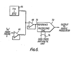
- This control of the drive signal to the phase modulator 26 may be achieved by the circuit arrangement shown in Figure 6.
- a voltage generator circuit 64 is provided which produces a variable DC signal having a voltage magnitude proportional to I/N+d.
- a buffer amplifier 66 is provided for receiving the enhanced representation of the ripple signal produced by the subsidiary phase lock loop 28. These signals are combined and fed via a further buffer amplifier 68 to the reference input terminal 70 of a multiplying D/A converter 72.
- the multiplying D/A converter 72 also receives data from the arithmetic unit 12 via a data bus 74.
- the multiplying D/A converter provides an output which is the product of these two inputs and this signal is used as the drive signal for the phase modulator 26.
- the 1/N+d proportional signal may be generated by known techniques such as providing a variable divider with a subsidiary output signal whose width is a constant number of input pulses. In a locked synthesiser this subsidiary output signal, when low pass filtered, will have a mean value proportional to 1/N+d.
- both phase lock loops may include a loop filter, and the reference input to the phase detector 34 may not be provided directly from the output from the phase modulator 26 to the phase detector 8 in the main phase lock loop. It is necessary only that the reference input to the subsidiary loop is dependent upon the signal afforded to the phase detector 8.
Landscapes
- Stabilization Of Oscillater, Synchronisation, Frequency Synthesizers (AREA)
Applications Claiming Priority (2)
| Application Number | Priority Date | Filing Date | Title |
|---|---|---|---|
| GB8503013 | 1985-02-06 | ||
| GB08503013A GB2173659B (en) | 1985-02-06 | 1985-02-06 | Frequency synthesisers |
Publications (2)
| Publication Number | Publication Date |
|---|---|
| EP0193273A2 true EP0193273A2 (fr) | 1986-09-03 |
| EP0193273A3 EP0193273A3 (fr) | 1988-08-31 |
Family
ID=10574043
Family Applications (1)
| Application Number | Title | Priority Date | Filing Date |
|---|---|---|---|
| EP86300512A Withdrawn EP0193273A3 (fr) | 1985-02-06 | 1986-01-27 | Synthétiseurs |
Country Status (5)
| Country | Link |
|---|---|
| US (1) | US4686488A (fr) |
| EP (1) | EP0193273A3 (fr) |
| JP (1) | JPS61245629A (fr) |
| AU (1) | AU579249B2 (fr) |
| GB (1) | GB2173659B (fr) |
Families Citing this family (47)
| Publication number | Priority date | Publication date | Assignee | Title |
|---|---|---|---|---|
| AU617455B2 (en) * | 1988-05-06 | 1991-11-28 | Alcatel N.V. | A digital frequency synthesizer |
| BE1001969A6 (nl) * | 1988-05-06 | 1990-04-24 | Bell Telephone Mfg Company N V | Numerieke modulator. |
| US4994768A (en) * | 1989-03-27 | 1991-02-19 | Motorola, Inc. | Frequency synthesizer with FM modulation |
| US5045813A (en) * | 1989-10-19 | 1991-09-03 | Nihon Musen Kabushiki Kaisha | Slip phase control PLL |
| SE465398B (sv) * | 1990-01-15 | 1991-09-02 | Ericsson Telefon Ab L M | Foerfarande och anordning foer frekvenssyntes |
| US5021754A (en) * | 1990-07-16 | 1991-06-04 | Motorola, Inc. | Fractional-N synthesizer having modulation spur compensation |
| FR2748872B1 (fr) * | 1990-08-21 | 1998-11-27 | Thomson Trt Defense | Synthetiseur de frequence a boucle a verrouillage de phase a division fractionnaire multiple |
| US5216374A (en) * | 1991-07-03 | 1993-06-01 | General Instrument Corporation | Frequency synthesizer utilizing pulse-width modulation of digital VCO control signal |
| US5224132A (en) * | 1992-01-17 | 1993-06-29 | Sciteq Electronics, Inc. | Programmable fractional-n frequency synthesizer |
| US5424688A (en) * | 1993-07-02 | 1995-06-13 | Rockwell International Corp. | Frequency synthesizer apparatus incorporating phase modulation tracking means |
| US5495206A (en) * | 1993-10-29 | 1996-02-27 | Motorola, Inc. | Fractional N frequency synthesis with residual error correction and method thereof |
| US5889436A (en) * | 1996-11-01 | 1999-03-30 | National Semiconductor Corporation | Phase locked loop fractional pulse swallowing frequency synthesizer |
| US7035607B2 (en) * | 1998-05-29 | 2006-04-25 | Silicon Laboratories Inc. | Systems and methods for providing an adjustable reference signal to RF circuitry |
| US6308055B1 (en) * | 1998-05-29 | 2001-10-23 | Silicon Laboratories, Inc. | Method and apparatus for operating a PLL for synthesizing high-frequency signals for wireless communications |
| US6574288B1 (en) | 1998-05-29 | 2003-06-03 | Silicon Laboratories Inc. | Method and apparatus for adjusting a digital control word to tune synthesized high-frequency signals for wireless communications |
| US6304146B1 (en) | 1998-05-29 | 2001-10-16 | Silicon Laboratories, Inc. | Method and apparatus for synthesizing dual band high-frequency signals for wireless communications |
| US6233441B1 (en) | 1998-05-29 | 2001-05-15 | Silicon Laboratories, Inc. | Method and apparatus for generating a discretely variable capacitance for synthesizing high-frequency signals for wireless communications |
| US6137372A (en) * | 1998-05-29 | 2000-10-24 | Silicon Laboratories Inc. | Method and apparatus for providing coarse and fine tuning control for synthesizing high-frequency signals for wireless communications |
| US6147567A (en) * | 1998-05-29 | 2000-11-14 | Silicon Laboratories Inc. | Method and apparatus for providing analog and digitally controlled capacitances for synthesizing high-frequency signals for wireless communications |
| US6150891A (en) | 1998-05-29 | 2000-11-21 | Silicon Laboratories, Inc. | PLL synthesizer having phase shifted control signals |
| US6226506B1 (en) | 1998-05-29 | 2001-05-01 | Silicon Laboratories, Inc. | Method and apparatus for eliminating floating voltage nodes within a discreetly variable capacitance used for synthesizing high-frequency signals for wireless communications |
| US6327463B1 (en) | 1998-05-29 | 2001-12-04 | Silicon Laboratories, Inc. | Method and apparatus for generating a variable capacitance for synthesizing high-frequency signals for wireless communications |
| US7221921B2 (en) * | 1998-05-29 | 2007-05-22 | Silicon Laboratories | Partitioning of radio-frequency apparatus |
| US6311050B1 (en) | 1998-05-29 | 2001-10-30 | Silicon Laboratories, Inc. | Single integrated circuit phase locked loop for synthesizing high-frequency signals for wireless communications and method for operating same |
| US7092675B2 (en) * | 1998-05-29 | 2006-08-15 | Silicon Laboratories | Apparatus and methods for generating radio frequencies in communication circuitry using multiple control signals |
| US6167245A (en) * | 1998-05-29 | 2000-12-26 | Silicon Laboratories, Inc. | Method and apparatus for operating a PLL with a phase detector/sample hold circuit for synthesizing high-frequency signals for wireless communications |
| US6993314B2 (en) | 1998-05-29 | 2006-01-31 | Silicon Laboratories Inc. | Apparatus for generating multiple radio frequencies in communication circuitry and associated methods |
| US7242912B2 (en) * | 1998-05-29 | 2007-07-10 | Silicon Laboratories Inc. | Partitioning of radio-frequency apparatus |
| US6064272A (en) * | 1998-07-01 | 2000-05-16 | Conexant Systems, Inc. | Phase interpolated fractional-N frequency synthesizer with on-chip tuning |
| JP4198833B2 (ja) * | 1999-07-23 | 2008-12-17 | 日本テキサス・インスツルメンツ株式会社 | 周波数シンセサイザ、リップルを補償する方法 |
| EP1133060B1 (fr) * | 2000-03-10 | 2005-08-17 | Koninklijke Philips Electronics N.V. | Boucle à verrouillage de phase permettant de générer un signal de référence ayant une grande pureté spectrale |
| US6323735B1 (en) | 2000-05-25 | 2001-11-27 | Silicon Laboratories, Inc. | Method and apparatus for synthesizing high-frequency signals utilizing on-package oscillator circuit inductors |
| US20030043950A1 (en) * | 2001-09-04 | 2003-03-06 | Hansen Eric J. | Phase-locked loop frequency synthesizer with two-point modulation |
| US6710951B1 (en) | 2001-10-31 | 2004-03-23 | Western Digital Technologies, Inc. | Phase locked loop employing a fractional frequency synthesizer as a variable oscillator |
| US8559587B1 (en) | 2012-03-21 | 2013-10-15 | Integrated Device Technology, Inc | Fractional-N dividers having divider modulation circuits therein with segmented accumulators |
| WO2014078311A2 (fr) * | 2012-11-14 | 2014-05-22 | Adeptence, Llc | Synthèse de fréquence utilisant une boucle à verrouillage de phase |
| US9236873B1 (en) | 2014-12-17 | 2016-01-12 | Integrated Device Technology, Inc. | Fractional divider based phase locked loops with digital noise cancellation |
| CN108701525B (zh) | 2016-07-27 | 2020-07-31 | 默升科技集团有限公司 | 适用于集成多信道接收器的增强型电感器 |
| US10723190B2 (en) * | 2016-11-29 | 2020-07-28 | Zhejiang CFMOTO Power Co., Ltd. | Rear swing arm suspension |
| US10483910B2 (en) | 2017-02-02 | 2019-11-19 | Credo Technology Group Limited | Multiport inductors for enhanced signal distribution |
| CN109314095B (zh) | 2017-04-10 | 2023-07-21 | 默升科技集团有限公司 | 笼式屏蔽中介层电感 |
| US10313105B2 (en) | 2017-09-12 | 2019-06-04 | Credo Technology Group Limited | Fractional-N PLL based clock recovery for SerDes |
| US10778236B2 (en) | 2019-01-04 | 2020-09-15 | Credo Technology Group Limited | PLL with wide frequency coverage |
| US11038602B1 (en) | 2020-02-05 | 2021-06-15 | Credo Technology Group Limited | On-chip jitter evaluation for SerDes |
| US10992501B1 (en) | 2020-03-31 | 2021-04-27 | Credo Technology Group Limited | Eye monitor for parallelized digital equalizers |
| US10892763B1 (en) * | 2020-05-14 | 2021-01-12 | Credo Technology Group Limited | Second-order clock recovery using three feedback paths |
| US12401488B1 (en) | 2024-03-28 | 2025-08-26 | Credo Technology Group Limited | Dynamic timing loop gain to compensate phase interpolation nonlinearities |
Family Cites Families (5)
| Publication number | Priority date | Publication date | Assignee | Title |
|---|---|---|---|---|
| JPS4864862A (fr) * | 1971-12-08 | 1973-09-07 | ||
| US3959737A (en) * | 1974-11-18 | 1976-05-25 | Engelmann Microwave Co. | Frequency synthesizer having fractional frequency divider in phase-locked loop |
| GB2097206B (en) * | 1981-04-21 | 1985-03-13 | Marconi Co Ltd | Frequency synthesisers |
| DE3214748A1 (de) * | 1982-04-21 | 1983-10-27 | Robert Bosch Gmbh, 7000 Stuttgart | Oszillatorschaltung |
| GB2140232B (en) * | 1983-05-17 | 1986-10-29 | Marconi Instruments Ltd | Frequency synthesisers |
-
1985
- 1985-02-06 GB GB08503013A patent/GB2173659B/en not_active Expired
-
1986
- 1986-01-27 EP EP86300512A patent/EP0193273A3/fr not_active Withdrawn
- 1986-01-31 US US06/824,805 patent/US4686488A/en not_active Expired - Fee Related
- 1986-02-06 JP JP61024917A patent/JPS61245629A/ja active Pending
- 1986-06-10 AU AU58520/86A patent/AU579249B2/en not_active Expired - Fee Related
Also Published As
| Publication number | Publication date |
|---|---|
| AU5852086A (en) | 1987-12-17 |
| EP0193273A3 (fr) | 1988-08-31 |
| GB8503013D0 (en) | 1985-03-06 |
| GB2173659B (en) | 1988-06-08 |
| AU579249B2 (en) | 1988-11-17 |
| JPS61245629A (ja) | 1986-10-31 |
| GB2173659A (en) | 1986-10-15 |
| US4686488A (en) | 1987-08-11 |
Similar Documents
| Publication | Publication Date | Title |
|---|---|---|
| US4686488A (en) | Fractional N frequency synthesizer with modulation compensation | |
| US4758802A (en) | Fractional N synthesizer | |
| US4516084A (en) | Frequency synthesizer using an arithmetic frequency synthesizer and plural phase locked loops | |
| US4888564A (en) | Phase-locked loop circuit | |
| EP0897616B1 (fr) | Synthetiseur de frequences a compensation de temperature et multiplication de frequence et son procede de fabrication | |
| US5038120A (en) | Frequency modulated phase locked loop with fractional divider and jitter compensation | |
| EP0453280B1 (fr) | Synthétiseur de fréquence à boucle à verrouillage de phase | |
| US6351485B1 (en) | Spread spectrum modulation technique for frequency synthesizers | |
| JPS6256689B2 (fr) | ||
| EP0622904B1 (fr) | Circuit PLL comportant plusieurs boucles, méthode de réception de signaux FM et dispositif les mettant en oeuvre | |
| US4603304A (en) | Reference frequency generation for split-comb frequency synthesizer | |
| US6049257A (en) | Method and arrangement for frequency modulation of a high-frequency signal | |
| US4682122A (en) | Frequency synthesizer stage adding high frequency steps to an initial frequency | |
| US3546617A (en) | Digital frequency synthesizer | |
| US4468632A (en) | Phase locked loop frequency synthesizer including fractional digital frequency divider | |
| US4464638A (en) | Universal digital frequency synthesizer using single side band techniques | |
| US4540945A (en) | Variable-frequency oscillation circuit | |
| US3902132A (en) | Closed loop variable frequency signal generator | |
| EP0378190A2 (fr) | Boucle d'asservissement de phase numérique | |
| JPH07143000A (ja) | 制御可能な発振器用の回路を使用する同期クロック生成方法 | |
| EP0173699B1 (fr) | Synthetiseur de frequence pilote de precision comportant un signal d'entree de frequence variable instable | |
| US4602219A (en) | Jitter reduction circuit for frequency synthesizer | |
| EP0566274A1 (fr) | Synthétiseur de fréquence utilisant une boucle à verrouillage de phase | |
| EP0497801B1 (fr) | Boucle a verrouillage de phase servant a produire une porteuse de reference pour un detecteur coherent | |
| US4186356A (en) | Phase locked loop frequency synthesizer and frequency modulator |
Legal Events
| Date | Code | Title | Description |
|---|---|---|---|
| PUAI | Public reference made under article 153(3) epc to a published international application that has entered the european phase |
Free format text: ORIGINAL CODE: 0009012 |
|
| AK | Designated contracting states |
Kind code of ref document: A2 Designated state(s): DE FR GB |
|
| PUAL | Search report despatched |
Free format text: ORIGINAL CODE: 0009013 |
|
| AK | Designated contracting states |
Kind code of ref document: A3 Designated state(s): DE FR GB |
|
| STAA | Information on the status of an ep patent application or granted ep patent |
Free format text: STATUS: THE APPLICATION HAS BEEN WITHDRAWN |
|
| 18W | Application withdrawn |
Withdrawal date: 19881122 |
|
| RIN1 | Information on inventor provided before grant (corrected) |
Inventor name: ATTENBOROUGH, COLIN |