EP0193304A2 - Herstellungsverfahren eines Bildfühlers - Google Patents
Herstellungsverfahren eines Bildfühlers Download PDFInfo
- Publication number
- EP0193304A2 EP0193304A2 EP86300928A EP86300928A EP0193304A2 EP 0193304 A2 EP0193304 A2 EP 0193304A2 EP 86300928 A EP86300928 A EP 86300928A EP 86300928 A EP86300928 A EP 86300928A EP 0193304 A2 EP0193304 A2 EP 0193304A2
- Authority
- EP
- European Patent Office
- Prior art keywords
- amorphous semiconductor
- layer
- prepared
- semiconductor layer
- amorphous
- Prior art date
- Legal status (The legal status is an assumption and is not a legal conclusion. Google has not performed a legal analysis and makes no representation as to the accuracy of the status listed.)
- Ceased
Links
Images


Classifications
-
- H—ELECTRICITY
- H10—SEMICONDUCTOR DEVICES; ELECTRIC SOLID-STATE DEVICES NOT OTHERWISE PROVIDED FOR
- H10F—INORGANIC SEMICONDUCTOR DEVICES SENSITIVE TO INFRARED RADIATION, LIGHT, ELECTROMAGNETIC RADIATION OF SHORTER WAVELENGTH OR CORPUSCULAR RADIATION
- H10F39/00—Integrated devices, or assemblies of multiple devices, comprising at least one element covered by group H10F30/00, e.g. radiation detectors comprising photodiode arrays
- H10F39/10—Integrated devices
- H10F39/12—Image sensors
- H10F39/191—Photoconductor image sensors
-
- H—ELECTRICITY
- H10—SEMICONDUCTOR DEVICES; ELECTRIC SOLID-STATE DEVICES NOT OTHERWISE PROVIDED FOR
- H10F—INORGANIC SEMICONDUCTOR DEVICES SENSITIVE TO INFRARED RADIATION, LIGHT, ELECTROMAGNETIC RADIATION OF SHORTER WAVELENGTH OR CORPUSCULAR RADIATION
- H10F39/00—Integrated devices, or assemblies of multiple devices, comprising at least one element covered by group H10F30/00, e.g. radiation detectors comprising photodiode arrays
- H10F39/011—Manufacture or treatment of image sensors covered by group H10F39/12
- H10F39/022—Manufacture or treatment of image sensors covered by group H10F39/12 of image sensors having active layers comprising only Group II-VI materials, e.g. CdS, ZnS or CdTe
-
- H—ELECTRICITY
- H10—SEMICONDUCTOR DEVICES; ELECTRIC SOLID-STATE DEVICES NOT OTHERWISE PROVIDED FOR
- H10F—INORGANIC SEMICONDUCTOR DEVICES SENSITIVE TO INFRARED RADIATION, LIGHT, ELECTROMAGNETIC RADIATION OF SHORTER WAVELENGTH OR CORPUSCULAR RADIATION
- H10F39/00—Integrated devices, or assemblies of multiple devices, comprising at least one element covered by group H10F30/00, e.g. radiation detectors comprising photodiode arrays
- H10F39/80—Constructional details of image sensors
- H10F39/805—Coatings
- H10F39/8057—Optical shielding
Definitions
- This invention relates to a method of manufacturing an image sensor by arranging a large number of photoelectric converting elements on a substrate, and, more particularly, to an image sensor manufacturing method which effectively reduces a leak current generated between the adjacent photoelectric converting elements.
- the degree of resolution constitutes one of particular importance.
- the conventional image sensor is accompanied with the drawbacks that, as the photoelectric converting elements are more closely arranged, a larger leak current is generated between the electrodes of the adjacent photoelectric converting elements. Consequently, sufficient improvement in resolution is not ensured, even if the photoelectric converting elements are densely arranged.
- a plurality of photoelectric converting elements are generally arranged on a substrate.
- the photoelectric converting element is constructed by arranging separate electrodes prepared from, for example, chromium, on a substrate; depositing an amorphous semiconductor layer 4 such as that prepared from amorphous hydrogenated silicon (a-Si:H) on said separate electrodes and substrate; forming a common electrode prepared from a transparent conductive layer prepared from, for example, indium tin oxide (ITO); and interposing said amorphous semiconductor layer between the separate electrodes and common electrode (a sandwich arrangement).
- amorphous semiconductor layer 4 such as that prepared from amorphous hydrogenated silicon (a-Si:H)
- photoelectric current Ip r conducted through the respective photoelectric converting elements by incoming light rays involves not only signal current I C which has a direc-' tional flow due to the presence of a potential barrier produced in an interface between the amorphous semiconductor layer and common electrode, but also leak current IL which has no directional flow due to the presence of a potential difference between respective individual electrodes 3-1, 3-2 and 3-3.
- Said leak current I L reduces the resolution degree of an image sensor.
- the object of this invention to provide a low cost method of manufacturing an image sensor so constructed as to effectively minimize the occurrence of a leak current between the adjacent photoelectric converting elements.
- this invention provides a method of manufacturing an image sensor by arranging, on a ceramic substrate, a plurality of individual electrodes, made of opaque metal materials, and a common electrode made of a transparent conductive layer, and interposing an amorphous semiconductor layers between said individual electrodes and common electrode, wherein regions defined between the respective photoelectric converting elements arranged on the amorphous semiconductor layers are enabled to have a high electric resistance when exposed to light.
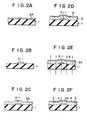
- Figs. 2A to 2F are sectional views showing the sequential steps of manufacturing an image sensor according to a first embodiment of this invention.
- individual electrodes 2-1, 2-2 and 2-3, composed of Cr are formed on said surface by thermal deposition or sputtering.
- Cr layer 2A shown in Fig. 2A is deposited to a thickness of about 3,000 A.
- Cr layer 2A is patterned into individual electrode 2-1 by the photoengraving process.
- band-shaped, amorphous semiconductor layer 3A prepared from, for example, hydrogenized amorphous silicon (a-Si:H), is mounted on substrate 1 and said individual electrode 2-1 by, for example, the plasma CVD process.
- transparent, conductive, common electrode 4 prepared from indium tin oxide (ITO), is, for example, sputtered on at least amorphous semiconductor layer 3.
- ITO indium tin oxide
- the image sensor fabricated by the steps shown up to Fig. 2D undergoes heating at a temperature higher than 100°C. When heating is brought to an end, the other side of the substrate is uniformly illuminated with about 200,000 luxes for about an hour, as shown in Fig. 2E.
- substrate 1 Since substrate 1 is transparent, light rays illuminated on said other side of substrate 1 permeate through it to the opposite side. In this case, light is not illuminated on that portion of amorphous semiconductor layer 3A which overlies said individual electrode 2-1. Those regions of amorphous semiconductor layer 3A which face the interstices between individual electrodes 2-1, 2-2 and 2-3, namely, the regions defined between respective photoelectric converting elements 7-1, 7-2 and 7-3 are exposed to light rays. As a result, those portions of amorphous semiconductor layer 3 which are illuminated by light rays are selectively formed into highly resistive regions 5 as shown in Fig. 2F.
- Figs. 3A and 3B indicate the structure of an image sensor manufactured through above-mentioned steps 2A to 2F.
- the portions of Figs. 3A and 3B the same as those of F ig. 2 are denoted by the same numerals.
- Reference numeral 6 denotes an auxiliary common electrode prepared from, for example, Cr. Though this auxiliary common electrode 6 is not always required, it is ordinarily formed on substrate 1 at the same time as individual electrodes 2-1, 2-2 and 2-3 in order to drop the electric resistance of common electrode 4, formed of a transparent conductive layer, thereby to minimize a voltage drop at this point.
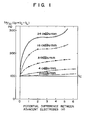
- the ratio of the leak current to the signal current indicates 2% when the image sensors are assembled with a density of 8/mm, 5% when the image sensor density shows 16/mm, and 5% when the image sensor density represents 24/mm, namely, the ratio of the leak current to the signal current is lower from what was observed in the conventional image sensor, to such extent that when adjacent electrodes are assembled to a density of 24/mm, the ratio does not exceed the practically applicable extent of 30%.
- the solid line of Fig. 5 represents the relationship between the ratio (Ip/I c ) of photocurrent Ip of the image sensors manufactured by the method of this invention and signal current I C running through said sensors, and the densities to which said image sensors are assembled.
- the broken line of Fig. 5 indicates a similar relationship observed in conventional image sensors which were manufactured without employing the light-exposure step shown in Fig. 2F.
- the data shown in Fig. 5 were obtained under the condition in which the potential difference between the adjacent electrodes was set at 1 V,' and the other factors were made to have the same values as those shown in Fig. 4.
- Fig. 5 indicates that the present invention noticeably reduces the ratio (I p /I C ) of leak current to signal current running through the adjacent image sensors to 1/15 of what is observed in the conventional image sensors.
- the present invention offers the advantages that the ratio between the leak current and signal current can be reduced to a one-digit value, and it is possible to easily manufacture image sensors at a higher density than 8/mm without fear that the properties of the image sensors will deteriorate and without need of the complicated step of precisely locating a mask between the light source and the image sensors.
- Figs. 6A to 6F of image sensors manufactured according to the above-mentioned second embodiment.
- transparent, common electrode membrane 12 is prepared-from, for example, indium tin oxide (ITO).
- ITO indium tin oxide
- amorphous semiconductor layer 13A is deposited on said common electrode layer 12.
- opaque metal layer 14A is mounted on amorphous semiconductor layer 13A.
- Said opaque metal layer 14A is patterned into individual electrode 14 by the photo etching process, as illustrated in Fig. 6D. Then as shown in F ig. 6 E , amorphous semiconductor layer 13A is exposed with light beams from the side of said individual electrode 14, thereby changing the regions interposed between the photoelectric converting elements mounted on amorphous semiconductor layer 13A into high electric resistive layers 15.
- Image sensors manufactured as in the above-mentioned second embodiment offer the same effect as those of the first embodiment. Since, in the second embodiment, an image is impressed on the photoelectric converting element through substrate 11, the substrate of the image sensors should also be prepared from transparent material.
- the present invention can be modified variously without departing from the scope and object of the invention.
- the amorphous semiconductor layer was prepared from hydrogenated amorphous silicon (a-Si:H).
- a-Si:H hydrogenated amorphous silicon
- any substance will of course attain the object, provided it gives the above-mentioned Staebler-Wronski effect. It is also possible to replace a-Si:H by a-S3.C:H, a-Si:F or F or a-Ge:H.
- the amorphous semiconductor layer admits of application to the present invention provided it contains at least one, for example, Ge selected from the elements belonging to Group IV of the periodic table and further at least one selected from the group consisting of H and F to act as a dangling bond.
- the proportions of the components such as H or F involved in the amorphous semiconductor membrane are preferred to range from 10 to 40 at.%.
- the present invention effectively reduces a leak current generated between the adjacent photoelectric converting elements.
- the image sensor embodying the present invention enables a leak current to be reduced to less than one-tenth of what is observed in the conventional image sensor manufactured without employing a step of restricting the leak current; namely, can manufacture high performance image sensors which enable a leak current to be noticeably minimized though they are assembled with great density.
Landscapes
- Solid State Image Pick-Up Elements (AREA)
- Facsimile Heads (AREA)
Applications Claiming Priority (2)
| Application Number | Priority Date | Filing Date | Title |
|---|---|---|---|
| JP60038055A JPS61198668A (ja) | 1985-02-27 | 1985-02-27 | イメ−ジセンサの製造方法 |
| JP38055/85 | 1985-02-27 |
Publications (2)
| Publication Number | Publication Date |
|---|---|
| EP0193304A2 true EP0193304A2 (de) | 1986-09-03 |
| EP0193304A3 EP0193304A3 (de) | 1989-03-15 |
Family
ID=12514821
Family Applications (1)
| Application Number | Title | Priority Date | Filing Date |
|---|---|---|---|
| EP86300928A Ceased EP0193304A3 (de) | 1985-02-27 | 1986-02-11 | Herstellungsverfahren eines Bildfühlers |
Country Status (3)
| Country | Link |
|---|---|
| US (1) | US4671853A (de) |
| EP (1) | EP0193304A3 (de) |
| JP (1) | JPS61198668A (de) |
Cited By (3)
| Publication number | Priority date | Publication date | Assignee | Title |
|---|---|---|---|---|
| EP0361481A3 (en) * | 1988-09-30 | 1990-11-14 | Kanegafuchi Chemical Industry Co., Ltd. | Method of stabilizing amorphous semiconductors, thus-stabilized amorphous semiconductors and devices using such semiconductors |
| EP0527373A1 (de) * | 1991-08-05 | 1993-02-17 | Siemens Aktiengesellschaft | Detektorsystem |
| WO1996004572A1 (en) * | 1994-08-02 | 1996-02-15 | Imperial College Of Science, Technology & Medicine | Ionizing radiation detector |
Families Citing this family (4)
| Publication number | Priority date | Publication date | Assignee | Title |
|---|---|---|---|---|
| US4951130A (en) * | 1987-04-30 | 1990-08-21 | Kabushiki Kaisha Toshiba | Color filter structure of color image sensor |
| US5288649A (en) * | 1991-09-30 | 1994-02-22 | Texas Instruments Incorporated | Method for forming uncooled infrared detector |
| US5449923A (en) * | 1992-03-31 | 1995-09-12 | Industrial Technology Research Institute | Amorphous silicon color detector |
| GB9509410D0 (en) * | 1995-05-10 | 1995-07-05 | Imperial College | Molecular imaging |
Family Cites Families (5)
| Publication number | Priority date | Publication date | Assignee | Title |
|---|---|---|---|---|
| US4371738A (en) * | 1981-05-04 | 1983-02-01 | Rca Corporation | Method of restoring degraded solar cells |
| JPS58130563A (ja) * | 1982-01-29 | 1983-08-04 | Seiko Epson Corp | イメ−ジセンサの製造方法 |
| JPS58195356A (ja) * | 1982-05-10 | 1983-11-14 | Nec Corp | 密着型イメ−ジセンサ |
| US4528065A (en) * | 1982-11-24 | 1985-07-09 | Semiconductor Energy Laboratory Co., Ltd. | Photoelectric conversion device and its manufacturing method |
| US4568409A (en) * | 1983-11-17 | 1986-02-04 | Chronar Corp. | Precision marking of layers |
-
1985
- 1985-02-27 JP JP60038055A patent/JPS61198668A/ja active Granted
-
1986
- 1986-02-11 EP EP86300928A patent/EP0193304A3/de not_active Ceased
- 1986-02-12 US US06/828,648 patent/US4671853A/en not_active Expired - Lifetime
Cited By (4)
| Publication number | Priority date | Publication date | Assignee | Title |
|---|---|---|---|---|
| EP0361481A3 (en) * | 1988-09-30 | 1990-11-14 | Kanegafuchi Chemical Industry Co., Ltd. | Method of stabilizing amorphous semiconductors, thus-stabilized amorphous semiconductors and devices using such semiconductors |
| EP0527373A1 (de) * | 1991-08-05 | 1993-02-17 | Siemens Aktiengesellschaft | Detektorsystem |
| WO1996004572A1 (en) * | 1994-08-02 | 1996-02-15 | Imperial College Of Science, Technology & Medicine | Ionizing radiation detector |
| US6072181A (en) * | 1994-08-02 | 2000-06-06 | Imperial College Of Science | Ionizing radiation detector |
Also Published As
| Publication number | Publication date |
|---|---|
| JPH0369186B2 (de) | 1991-10-31 |
| US4671853A (en) | 1987-06-09 |
| EP0193304A3 (de) | 1989-03-15 |
| JPS61198668A (ja) | 1986-09-03 |
Similar Documents
| Publication | Publication Date | Title |
|---|---|---|
| EP0060699B1 (de) | Verfahren zur Herstellung von lichtempfindlichen Sensoren | |
| CA1125894A (en) | Photosensor | |
| US4405915A (en) | Photoelectric transducing element | |
| US4650984A (en) | Photosensor array for treating image information | |
| JPS59143362A (ja) | パツシベ−シヨン膜 | |
| US4671853A (en) | Image sensor manufacturing method | |
| US4791466A (en) | Line scanner image sensor | |
| US4719348A (en) | Optical sensor having heating element to heat amorphous semiconductor film | |
| JPS5840856A (ja) | 光センサアレイ | |
| US5084399A (en) | Semi conductor device and process for fabrication of same | |
| JPS6327871B2 (de) | ||
| JPH0564468B2 (de) | ||
| JPS6322465B2 (de) | ||
| JPS61292959A (ja) | イメ−ジセンサの製造方法 | |
| JP2889963B2 (ja) | 密着型イメージセンサ | |
| KR910005603B1 (ko) | 광전 변환 장치 | |
| KR820002330B1 (ko) | 수광소자(受光素子) | |
| JP2910227B2 (ja) | 密着型イメージセンサの製造方法 | |
| JPS61156766A (ja) | イメ−ジセンサ | |
| JP2661689B2 (ja) | 光センサ | |
| JPS6251257A (ja) | イメ−ジセンサの製造方法 | |
| JPH021166A (ja) | 密着型イメージセンサ | |
| JPS62252968A (ja) | 非晶質シリコンイメ−ジセンサ | |
| JPS63119259A (ja) | アモルフアスシリコンホトダイオ−ドアレイ | |
| JPS63314863A (ja) | 受光素子アレイ |
Legal Events
| Date | Code | Title | Description |
|---|---|---|---|
| PUAI | Public reference made under article 153(3) epc to a published international application that has entered the european phase |
Free format text: ORIGINAL CODE: 0009012 |
|
| 17P | Request for examination filed |
Effective date: 19860214 |
|
| AK | Designated contracting states |
Kind code of ref document: A2 Designated state(s): DE FR GB |
|
| PUAL | Search report despatched |
Free format text: ORIGINAL CODE: 0009013 |
|
| AK | Designated contracting states |
Kind code of ref document: A3 Designated state(s): DE FR GB |
|
| 17Q | First examination report despatched |
Effective date: 19910531 |
|
| STAA | Information on the status of an ep patent application or granted ep patent |
Free format text: STATUS: THE APPLICATION HAS BEEN REFUSED |
|
| 18R | Application refused |
Effective date: 19911125 |
|
| RIN1 | Information on inventor provided before grant (corrected) |
Inventor name: TAKAYAMA, SATOSHIC/O PATENT DIVISION |