EP0194205A2 - Verfahren zum Herstellen eines Einzelchip-Mikrocomputers - Google Patents
Verfahren zum Herstellen eines Einzelchip-Mikrocomputers Download PDFInfo
- Publication number
- EP0194205A2 EP0194205A2 EP86400480A EP86400480A EP0194205A2 EP 0194205 A2 EP0194205 A2 EP 0194205A2 EP 86400480 A EP86400480 A EP 86400480A EP 86400480 A EP86400480 A EP 86400480A EP 0194205 A2 EP0194205 A2 EP 0194205A2
- Authority
- EP
- European Patent Office
- Prior art keywords
- bonding pads
- chip
- masks
- patterns
- wirings
- Prior art date
- Legal status (The legal status is an assumption and is not a legal conclusion. Google has not performed a legal analysis and makes no representation as to the accuracy of the status listed.)
- Granted
Links
Images



Classifications
-
- H—ELECTRICITY
- H10—SEMICONDUCTOR DEVICES; ELECTRIC SOLID-STATE DEVICES NOT OTHERWISE PROVIDED FOR
- H10W—GENERIC PACKAGES, INTERCONNECTIONS, CONNECTORS OR OTHER CONSTRUCTIONAL DETAILS OF DEVICES COVERED BY CLASS H10
- H10W20/00—Interconnections in chips, wafers or substrates
- H10W20/01—Manufacture or treatment
-
- H—ELECTRICITY
- H10—SEMICONDUCTOR DEVICES; ELECTRIC SOLID-STATE DEVICES NOT OTHERWISE PROVIDED FOR
- H10W—GENERIC PACKAGES, INTERCONNECTIONS, CONNECTORS OR OTHER CONSTRUCTIONAL DETAILS OF DEVICES COVERED BY CLASS H10
- H10W20/00—Interconnections in chips, wafers or substrates
- H10W20/40—Interconnections external to wafers or substrates, e.g. back-end-of-line [BEOL] metallisations or vias connecting to gate electrodes
- H10W20/41—Interconnections external to wafers or substrates, e.g. back-end-of-line [BEOL] metallisations or vias connecting to gate electrodes characterised by their conductive parts
- H10W20/43—Layouts of interconnections
-
- H—ELECTRICITY
- H10—SEMICONDUCTOR DEVICES; ELECTRIC SOLID-STATE DEVICES NOT OTHERWISE PROVIDED FOR
- H10W—GENERIC PACKAGES, INTERCONNECTIONS, CONNECTORS OR OTHER CONSTRUCTIONAL DETAILS OF DEVICES COVERED BY CLASS H10
- H10W72/00—Interconnections or connectors in packages
- H10W72/071—Connecting or disconnecting
- H10W72/073—Connecting or disconnecting of die-attach connectors
-
- H—ELECTRICITY
- H10—SEMICONDUCTOR DEVICES; ELECTRIC SOLID-STATE DEVICES NOT OTHERWISE PROVIDED FOR
- H10W—GENERIC PACKAGES, INTERCONNECTIONS, CONNECTORS OR OTHER CONSTRUCTIONAL DETAILS OF DEVICES COVERED BY CLASS H10
- H10W72/00—Interconnections or connectors in packages
- H10W72/90—Bond pads, in general
-
- H—ELECTRICITY
- H10—SEMICONDUCTOR DEVICES; ELECTRIC SOLID-STATE DEVICES NOT OTHERWISE PROVIDED FOR
- H10W—GENERIC PACKAGES, INTERCONNECTIONS, CONNECTORS OR OTHER CONSTRUCTIONAL DETAILS OF DEVICES COVERED BY CLASS H10
- H10W90/00—Package configurations
-
- H—ELECTRICITY
- H10—SEMICONDUCTOR DEVICES; ELECTRIC SOLID-STATE DEVICES NOT OTHERWISE PROVIDED FOR
- H10W—GENERIC PACKAGES, INTERCONNECTIONS, CONNECTORS OR OTHER CONSTRUCTIONAL DETAILS OF DEVICES COVERED BY CLASS H10
- H10W90/00—Package configurations
- H10W90/701—Package configurations characterised by the relative positions of pads or connectors relative to package parts
- H10W90/751—Package configurations characterised by the relative positions of pads or connectors relative to package parts of bond wires
- H10W90/754—Package configurations characterised by the relative positions of pads or connectors relative to package parts of bond wires between a chip and a stacked insulating package substrate, interposer or RDL
-
- Y—GENERAL TAGGING OF NEW TECHNOLOGICAL DEVELOPMENTS; GENERAL TAGGING OF CROSS-SECTIONAL TECHNOLOGIES SPANNING OVER SEVERAL SECTIONS OF THE IPC; TECHNICAL SUBJECTS COVERED BY FORMER USPC CROSS-REFERENCE ART COLLECTIONS [XRACs] AND DIGESTS
- Y10—TECHNICAL SUBJECTS COVERED BY FORMER USPC
- Y10S—TECHNICAL SUBJECTS COVERED BY FORMER USPC CROSS-REFERENCE ART COLLECTIONS [XRACs] AND DIGESTS
- Y10S257/00—Active solid-state devices, e.g. transistors, solid-state diodes
- Y10S257/923—Active solid-state devices, e.g. transistors, solid-state diodes with means to optimize electrical conductor current carrying capacity, e.g. particular conductor aspect ratio
Definitions
- the present invention relates to the fabrication of a 1- chip microcomputer, in particular, to the fabrication of a chip referred to as an evaluation chip which is used for evaluating a program built in a 1-chip microcomputer to be mass-produced.
- Microcomputers have been used for controlling the operations of various industrial equipment and consumer applicances.
- the microcomputer used for these applications is a 1-chip microcomputer in which facilities including logic circuits and memory devices are integrated on a semiconductor chip.
- Such a 1-chip microcomputer comprises a ROM (Read Only Memory) for storing a program under which the operation of the microcomputer is controlled.
- the program is developed according to the-functions provided for the equipment and so forth; therefore, it is different with each user of the 1-chip microcomputer.
- EPROM Erasable Programmable ROM
- the program must be completely debugged and subjected to functional tests in advance, since it cannot be modified once written in the ROM.
- an evaluation chip is prepared in advance.
- the evaluation chip is usually fabricated based on the design resources of a 1-chip microcomputer to be mass-produced, wherein an external memory device is used to substitute for the ROM for storing the program.
- the program can be subjected to modifications as many times as required according to the results of the functional tests.
- the evaluation chip is provided with an interface circuit including address output buffer and data input buffer. The configuration of a conven- tonal evaluation chip will be explained in the following in comparison with that of a chip of the corresponding 1-chip microcomputer to be mass-produced.
- Fig. 1 is a schematic plan view of an exemplary arrangement of facilities formed in a chip 20 of a 1 -chip microcomputer, the facilities including a RAM (Random Access Memory), registers REG, logic circuits LOGIC, a clock generator CLK, an instruction programmable logic array IPLA, a program counter PC and a ROM.
- RAM Random Access Memory
- ROM When receiving an address signal from PC, ROM outputs a corresponding data or an instruction stored therein to IPLA.
- these facilities are represented as the respective regions allotted for them on the chip 20 and it will be done so in the following drawings. Also in Fig. 1, only connections 22 and 23 relevant to the respective transmissions of the address and data signals are illustrated.
- the data consists of parallel eight bits, but the number of the address bits differs depending on the capacity of the ROM; 10 bits for a ROM of 1 K bits, for instance.
- a number of bonding pads 21, which are referred to as first bonding pads hereinafter, are formed at the periphery of the chip 20.
- the first bonding pads 21 are usually arranged in an array surrounding the facilities. Each of the first bonding pads 21 is connected to one of the facilities with a corresponding wiring (not shown).
- the first bonding pads 21 are disposed with a constant pitch due to the general requirement of automatic bonding machines.
- Fig. 2 is a schematic plan view of an exemplary configuration of a conventional evaluation chip for the 1- chip microcomputer shown in Fig. 1.
- the evaluation chip 30 has an extended area around an inner area indicated by a dot-dash line.
- the inner area is referred to as a device area hereinafter, in which the same facilities as. in the 1-chip microcomputer of Fig. 1, except for the ROM, are formed.
- the arrangement of these facilities in the device area is substantially the same as in the 1-chip microcomputer shown in Fig. 1.
- the bonding pads 31 corresponding to the first bonding pads 21 in Fig.1 are formed in the extended area instead of the device area and connected to the facilities via wirings not shown.
- the region 36 allotted for the ROM of the 1-chip microcomputer is blank, and an address output buffer 34 and a data input buffer 35 are provided in the extended area of the chip 30 instead.
- the region 36 is referred to as a ROM region hereinafter.
- the address output buffer 34 and data input buffer 35 are connected to PC and IPLA, respectively, via respective wirings 32 and 33 and allow the evaluation chip to have an access to an external memory device for storing the program to be evaluated.
- the masks for fabricating the evaluation chip can be produced based on the existing masks prepared for the mass-production chips of the 1-chip microcomputer, said existing masks being modified by adding patterns necessary for forming the buffers 34 and 35 and the wirings 32 and 33, and by changing the arrangement of the bonding pads 31 and the connections between the bonding pads 31 and the facilities in the device region.
- the bonding pads 31 include incremental pads 310 for connecting the buffers 34 and 35 to the aforesaid external memory device (not shown).
- the total number of the incremental bonding pads 310 amounts to 18, for instance.
- the evaluation chip 30 is generally designed to have an extended area compared with the mass-production chip of Fig.1.
- the facilities formed in the device area are arranged and interconnected with each other substantially as in the 1-chip microcomputer shown in Fig. 1.
- the pads 31 and 310 must be disposed with a constant pitch because of the above mentioned reason. Therefore, when the total number of bonding pads 31 is increased due to the incremental pads 310, the relative arrangement of the pads 31 with respect to the facilities cannot remain as in the 1-chip microcomputer.
- the modification in the masks for fabricating the conventional evaluation chip is not limited to the addition of the buffers 34 and 35 together with the incremental bonding pads 310 and wirings 32 and 33 but involves a comprehensive redesign in the wiring pattern for connecting the bonding pads 31 to the facilities.
- the conventional evaluation chip must be designed to have a margin for the chip area thereof so as to permit the wirings 32 and 33 to be distributed without intersecting the existing wirings.
- the margin is already provided in the mass-production chips, the chip area utilization efficiency is decreased.
- the layout in the mass-production chip is optimized and the margin must be afforded in the evaluation chip, the aforesaid redesign in the wiring pattern inevitably becomes further complicated.
- an object of the present invention to provide an efficent fabrication method for an evaluation chip of a 1-chip microcomputer.
- Fig. 3 is a schematic plan view of an exemplary arrangement of patterns formed on an evaluation chip in accordance with a first embodiment of the present invention.
- chip 40 of a semiconductor substrate has facilities including a RAM, registers REG, logic circuits LOGIC, a clock generator CLK, an instruction programmable logic array IPLA, and a program counter PC, all the same as in a corresponding 1-chip microcomputer, except for a ROM to be formed in the region 36.
- These facilities are arranged in a device area, which is enclosed by a virtual dot-dash line, and interconnected with each other by means of wirings not shown, except wirings 22 and 23.
- Some of the facilities are connected to first bonding pads 21 formed at the periphery of the device area by means of wirings (not shown).
- the pattern of the interconnections between the facilities and the respective connections between the same facilities and the first bonding pads 21 are quite the same as in the corresponding 1-chip microcomputer shown in Fig. 1.
- the chip 40 is provided with an extended area around the device area.
- the aforesaid address output buffer 34 and data input buffer 35 are formed in the ROM region 36.
- the inputs of the address output buffer 3 4 are connected to the program counter PC by means of wirings (a bus line) 22 and the outputs of the data input buffer 35 are connected to the instruction programmable logic array IPLA by means of wirings (a bus line) 23.
- the wirings 22 and 23 are formed quite the same as in the 1-chip microcomputer of Fig. 1.
- second bonding pads 41 which are formed in a number larger than that of the first bonding pads 2 1 by the number necessary for the connections to the wirings 22 and 23.
- the second bonding pads 41 are disposed with a substantially constant pitch so as to comply with the requirement of automatic bonding machines. Most of the second bonding pads 41 are connected to the first pads 21, preferably to the respective nearest ones, by means of corresponding wirings 44 and the remaining second bonding pads are connected to the outputs of the address output buffer 34 and to the inputs of the data input buffer 35 by means of respective wirings (bus lines) 42 and 43. Thus, the first bonding pads 21 and the corresponding second bonding pads 41 can be interconnected by relatively short and simple wirings 44.
- patterns for the facilities and wirings in a 1-chip microcomputer can be used for producing masks for the corresponding evaluation chip, except for the ROM region.
- the evaluation chip can be designed only by replacing the ROM pattern in each of the masks for the 1-chip microcomputer by respective patterns for forming address output and data input buffers, and by adding patterns for providing the second bonding pads and wirings connecting the second bonding pads to the buffers and the first bonding pads. Accordingly, the fabrication of an evaluation chip can be facilitated and shows an enhanced reliability compared with the prior art method explained with reference to Fig. 2.
- the present invention allows an efficient use of the chip area because the address output and data input buffers are formed in the ROM region 36 which is not utilized in the conventional evaluation chip shown in Fig. 2, and the extended area around the device area can be as small as possible, so far as it can accommodate the second bonding pads and the wirings connected thereto.
- Fig. 4 is a schematic plan view illustrating an exemplary arrangement of patterns formed on an evaluation chip in accordance with a second embodiment of the present invention, wherein a multiple-layer wiring technology is employed for the aforesaid second bonding pads and wirings connected thereto.
- Fig. 4 only an address output buffer 5 and data input buffer 6 both formed in a region 4 on an evaluation chip 1 are shown and other facilities are omitted from the illustration.
- the region 4 is allotted for the ROM in the corresponding mass-production chip.
- the address output and data input buffers 5 and 6 are connected to respective groups of second bonding pads 7, a first group consisting of A o to A, and a second group l o to 17, by wirings 12 and 13, respectively.
- the wirings for interconnecting the not shown facilities and first bonding pads 8' in a device area 2 enclosed by a dot-dash line are formed exactly as in the corresponding mass-production chip.
- Each of the first bonding pads 8' is connected to a respective one of the second bonding pads 7 by a corresponding wiring 9.
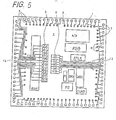
- Fig. 5 is a schematic plan view illustrating a further detailed arrangement of patterns formed on an evaluation chip in accordance with a third embodiment of the present invention.
- additional facilities including a random access memory RAM, an analog-to-digital converter A/D, a stack register STACK and a prescaler PS are formed in a not-indicated device area on an evaluation chip 1.
- the address output buffer 5 comprises elemental circuits A o to A" and the data input buffer 6 comprises elemental circuits l o to 1,. Each of these elemental circuits is connected to a corresponding one of second bonding pads 7 via a respective one of wirings 12 and 13.
- the patterns of the respective internal wirings of the address output buffer 5 and data input bufer 6 to a lower wiring layer which is selected to form therein the internal wirings of the facilities and the first bonding pads 8, and to add patterns of the second bonding pads 7 and wirings 9, 12 and 13, all connected to the second bonding pads 7, to an upper wiring layer which is selected to form therein interconnections between the facilities.
- the latter wiring layer is uppermost.
- Figs. 6A and 68 are a schematic partial plan view and a cross-section of an evaluation chip fabricated according to the second or third embodiment, illustrating first and second bonding pads and wirings connected thereto, which are formed by using a double-layer wiring configuration.
- the first bonding pad 8 and a wiring 10 connecting a diffusion region 101 to the first bonding pad 8 are formed from the lower layer of the double-layer wiring configuration.
- the diffusion region 101 formed in a semiconductor substrate 1' which constitutes the evaluation chip is a part of one of the facilities formed in the device area 2.
- the second bonding pad 7 formed at the extended area 3 of the evaluation chip and a wiring 9 interconnecting the first bonding pad 8 and the second bonding pad 7 are formed from the upper layer of the double-layer wiring configuration.
- the lower wiring layer is isolated from the substrate 1' by a dielectric layer 201.
- Another dialectric layer 202 is formed to isolate the lower and upper wiring layers from each other.
- the bonding pad 7 can be provide with an external connection through a window formed in a passivation layer 203.
- Figs. 7A and 7B are a schematic partial plan view and a cross-section of an evaluation chip fabricated according to the second or third embodiment, illustrating a second bonding pad and two wirings formed by using a double-layer- wiring configuration.
- the second bonding pad 7 formed in the extended area 3 of the evaluation chip is connected to a diffusion layer 102 formed in the device area 2 via a wiring 12 (13).
- the diffusion region 102 which is formed in a semiconductor substrate 1' constituting the evaluation chip is a part of a buffer circuit formed in the ROM region 4.
- the second bonding pad 7 and wiring 12 - (13) are formed from the upper layer of the double-layer wiring configuration.
- the wiring 12 (13) intersects another wiring 11 formed from the lower layer of the double-layer wiring configuration.
- the wiring 11 is designed for interconnecting diffusion regions 103 and 10 4 , each of which constitutes a part of a respective facility formed in the device area 2.
- the wiring 11 is isolated from the substrate 1' by a dielectric layer 201.
- the wirings 11 and 12 (13) are insulated from each other by another dielectric layer 202.
- the second bonding pad 7 can be provided with an external connection through a window formed in a passivation layer 203.
- the method according to the present invention allows elimination of the need for modifications in the arrangement of the facilities and in the pattern of wirings interconnecting same, which are designed for the mass-production of a 1-chip microcomputer, when an evaluation chip is fabricated based on the mask patterns designed for the mass-production chips, hence, simplifies the wirings for the external connections thereof and minimizes erroneous wirings in the evaluation chip.
- the productivity and reliability in the fabrication of the evaluation chip are thereby enhanced.
- the above together with the forming of the interface means for the external memory device in the ROM region permits the increase of efficiency of area utilization in both of the mass-production and evaluation chips.
Landscapes
- Semiconductor Integrated Circuits (AREA)
- Design And Manufacture Of Integrated Circuits (AREA)
Applications Claiming Priority (2)
| Application Number | Priority Date | Filing Date | Title |
|---|---|---|---|
| JP60045808A JPS61222148A (ja) | 1985-03-08 | 1985-03-08 | 1チツプマイクロコンピユ−タの製造方法 |
| JP45808/85 | 1985-03-08 |
Publications (3)
| Publication Number | Publication Date |
|---|---|
| EP0194205A2 true EP0194205A2 (de) | 1986-09-10 |
| EP0194205A3 EP0194205A3 (en) | 1987-10-07 |
| EP0194205B1 EP0194205B1 (de) | 1990-10-24 |
Family
ID=12729555
Family Applications (1)
| Application Number | Title | Priority Date | Filing Date |
|---|---|---|---|
| EP86400480A Expired - Lifetime EP0194205B1 (de) | 1985-03-08 | 1986-03-07 | Verfahren zum Herstellen eines Einzelchip-Mikrocomputers |
Country Status (5)
| Country | Link |
|---|---|
| US (1) | US4833620A (de) |
| EP (1) | EP0194205B1 (de) |
| JP (1) | JPS61222148A (de) |
| KR (1) | KR900008017B1 (de) |
| DE (1) | DE3675038D1 (de) |
Cited By (3)
| Publication number | Priority date | Publication date | Assignee | Title |
|---|---|---|---|---|
| EP0407268A1 (de) * | 1989-07-07 | 1991-01-09 | STMicroelectronics S.A. | Integrierte Schaltung mit Mikroprozessor und programmierbarer innerer Uhr |
| EP0588577A3 (de) * | 1992-09-14 | 1994-04-20 | Dow Corning Corporation | Hermetisch abgedichtete integrierte Schaltungen |
| WO2002093640A1 (fr) * | 2001-05-12 | 2002-11-21 | Advantest Corporation | Procede d'evaluation de systeme-sur-puce (soc) presentant un noyau en tant que base, et structure soc faisant intervenir le procede d'evaluation |
Families Citing this family (12)
| Publication number | Priority date | Publication date | Assignee | Title |
|---|---|---|---|---|
| GB2214334B (en) * | 1988-01-05 | 1992-05-06 | Texas Instruments Ltd | Integrated circuit |
| US5270944A (en) * | 1988-06-09 | 1993-12-14 | Hitachi, Ltd. | Semiconductor integrated circuit device and process for manufacturing the same |
| US5182719A (en) * | 1988-06-09 | 1993-01-26 | Hitachi, Ltd. | Method of fabricating a second semiconductor integrated circuit device from a first semiconductor integrated circuit device |
| JPH02197160A (ja) * | 1989-01-26 | 1990-08-03 | Nec Corp | Lsi基板 |
| US4936334A (en) * | 1989-09-29 | 1990-06-26 | Allied-Signal Inc. | Differential pressure shuttle valve |
| US5119158A (en) * | 1989-11-21 | 1992-06-02 | Nec Corporation | Gate array semiconductor integrated circuit device |
| JP2531827B2 (ja) * | 1990-04-25 | 1996-09-04 | 株式会社東芝 | 半導体装置及びその製造方法 |
| US5493723A (en) * | 1990-11-06 | 1996-02-20 | National Semiconductor Corporation | Processor with in-system emulation circuitry which uses the same group of terminals to output program counter bits |
| JP2925337B2 (ja) * | 1990-12-27 | 1999-07-28 | 株式会社東芝 | 半導体装置 |
| US6223146B1 (en) * | 1994-06-29 | 2001-04-24 | Kelsey-Hayes Company | Method and apparatus for manufacturing a programmed electronic control unit for use in an anti-lock braking (ABS) system |
| US6820246B2 (en) * | 2001-02-28 | 2004-11-16 | Sanyo Electric Co., Ltd. | Pattern layout method of semiconductor device |
| KR101883152B1 (ko) | 2011-08-04 | 2018-08-01 | 삼성전자 주식회사 | 반도체 장치 |
Family Cites Families (6)
| Publication number | Priority date | Publication date | Assignee | Title |
|---|---|---|---|---|
| DE3273507D1 (en) * | 1981-03-20 | 1986-11-06 | Fujitsu Ltd | A one chip microcomputer |
| JPS57212563A (en) * | 1981-06-25 | 1982-12-27 | Fujitsu Ltd | Address reading circuit for one-chip microcomputer |
| JPS59146352A (ja) * | 1983-02-09 | 1984-08-22 | Nec Corp | シングル・チップ・マイクロコンピュータ |
| EP0127100B1 (de) * | 1983-05-24 | 1990-04-11 | Kabushiki Kaisha Toshiba | Integrierte Halbleiterschaltungsanordnung |
| JPS6089955A (ja) * | 1983-10-21 | 1985-05-20 | Mitsubishi Electric Corp | 半導体装置 |
| JPS6151695A (ja) * | 1984-08-22 | 1986-03-14 | Hitachi Ltd | 半導体集積回路装置 |
-
1985
- 1985-03-08 JP JP60045808A patent/JPS61222148A/ja active Granted
-
1986
- 1986-03-06 US US06/836,752 patent/US4833620A/en not_active Expired - Fee Related
- 1986-03-07 EP EP86400480A patent/EP0194205B1/de not_active Expired - Lifetime
- 1986-03-07 KR KR1019860001628A patent/KR900008017B1/ko not_active Expired
- 1986-03-07 DE DE8686400480T patent/DE3675038D1/de not_active Expired - Lifetime
Cited By (5)
| Publication number | Priority date | Publication date | Assignee | Title |
|---|---|---|---|---|
| EP0407268A1 (de) * | 1989-07-07 | 1991-01-09 | STMicroelectronics S.A. | Integrierte Schaltung mit Mikroprozessor und programmierbarer innerer Uhr |
| FR2649504A1 (fr) * | 1989-07-07 | 1991-01-11 | Sgs Thomson Microelectronics | Circuit integre a microprocesseur et horloge interne programmable |
| US5036300A (en) * | 1989-07-07 | 1991-07-30 | Sgs-Thomson Microelectronics S.A. | Integrated circuit with microprocessor and programmable internal clock |
| EP0588577A3 (de) * | 1992-09-14 | 1994-04-20 | Dow Corning Corporation | Hermetisch abgedichtete integrierte Schaltungen |
| WO2002093640A1 (fr) * | 2001-05-12 | 2002-11-21 | Advantest Corporation | Procede d'evaluation de systeme-sur-puce (soc) presentant un noyau en tant que base, et structure soc faisant intervenir le procede d'evaluation |
Also Published As
| Publication number | Publication date |
|---|---|
| KR900008017B1 (ko) | 1990-10-29 |
| EP0194205B1 (de) | 1990-10-24 |
| EP0194205A3 (en) | 1987-10-07 |
| US4833620A (en) | 1989-05-23 |
| JPS61222148A (ja) | 1986-10-02 |
| DE3675038D1 (de) | 1990-11-29 |
| KR860007743A (ko) | 1986-10-17 |
| JPH0367342B2 (de) | 1991-10-22 |
Similar Documents
| Publication | Publication Date | Title |
|---|---|---|
| EP0194205B1 (de) | Verfahren zum Herstellen eines Einzelchip-Mikrocomputers | |
| EP0073641B1 (de) | Integrierte Schaltungsvorrichtung | |
| EP0257437B1 (de) | Integrierte Schaltung in Hauptscheibentechnik | |
| US4612618A (en) | Hierarchical, computerized design of integrated circuits | |
| US5805865A (en) | Semiconductor device | |
| EP0219413A2 (de) | Matrixrekonfigurationsgerät und Verfahren, insbesondere angepasst zum Gebrauch mit LSI-Schaltungen | |
| US6516446B2 (en) | Design system for flip chip semiconductor device | |
| US20130283224A1 (en) | Method and apparatus of an integrated circuit | |
| EP0791963B1 (de) | Integrierte Schaltung mit Gate-Array-Verbindungen, die über das Speichergebiet geführt werden | |
| US4942317A (en) | Master slice type semiconductor integrated circuit having 2 or more I/O cells per connection pad | |
| US5952684A (en) | Chip layout of semiconductor integrated circuit | |
| JPH0259490B2 (de) | ||
| EP0408060A2 (de) | Integrierte Halbleiterschaltungsanordnung und Verfahren zu deren Logikkorrektur | |
| US4858175A (en) | Monolithic semi-custom IC having standard LSI sections and coupling gate array sections | |
| EP0609047A2 (de) | Verfahren zur Herstellung einer anwendungsspezifischen integrierten Schaltung (ASIC) mit einem Gate-Array-Funktionsblock | |
| KR101116325B1 (ko) | 반도체 장치 | |
| EP0422930A2 (de) | Integrierte Halbleiter-Schaltungs-Vorrichtungen | |
| JPS62273751A (ja) | 集積回路 | |
| KR900008796B1 (ko) | 반주문형 시스템 lsi | |
| US5763944A (en) | Semiconductor device having a reduced wiring area in and out of data path zone | |
| KR0135237B1 (ko) | 반도체 장치 | |
| JPH04246857A (ja) | 半導体集積回路装置 | |
| Maloberti | Silicon implementation of multiprocessor pyramid architecture | |
| KR900000563B1 (ko) | 반주문형 시스템 lsi | |
| Aakhus et al. | ACCLAIM—a computer aided design system |
Legal Events
| Date | Code | Title | Description |
|---|---|---|---|
| PUAI | Public reference made under article 153(3) epc to a published international application that has entered the european phase |
Free format text: ORIGINAL CODE: 0009012 |
|
| AK | Designated contracting states |
Kind code of ref document: A2 Designated state(s): DE FR GB |
|
| PUAL | Search report despatched |
Free format text: ORIGINAL CODE: 0009013 |
|
| AK | Designated contracting states |
Kind code of ref document: A3 Designated state(s): DE FR GB |
|
| 17P | Request for examination filed |
Effective date: 19880205 |
|
| 17Q | First examination report despatched |
Effective date: 19891218 |
|
| GRAA | (expected) grant |
Free format text: ORIGINAL CODE: 0009210 |
|
| AK | Designated contracting states |
Kind code of ref document: B1 Designated state(s): DE FR GB |
|
| REF | Corresponds to: |
Ref document number: 3675038 Country of ref document: DE Date of ref document: 19901129 |
|
| ET | Fr: translation filed | ||
| PLBE | No opposition filed within time limit |
Free format text: ORIGINAL CODE: 0009261 |
|
| STAA | Information on the status of an ep patent application or granted ep patent |
Free format text: STATUS: NO OPPOSITION FILED WITHIN TIME LIMIT |
|
| 26N | No opposition filed | ||
| PGFP | Annual fee paid to national office [announced via postgrant information from national office to epo] |
Ref country code: GB Payment date: 19930105 Year of fee payment: 8 |
|
| PGFP | Annual fee paid to national office [announced via postgrant information from national office to epo] |
Ref country code: FR Payment date: 19930330 Year of fee payment: 8 |
|
| PGFP | Annual fee paid to national office [announced via postgrant information from national office to epo] |
Ref country code: DE Payment date: 19930521 Year of fee payment: 8 |
|
| PG25 | Lapsed in a contracting state [announced via postgrant information from national office to epo] |
Ref country code: GB Effective date: 19940307 |
|
| GBPC | Gb: european patent ceased through non-payment of renewal fee |
Effective date: 19940307 |
|
| PG25 | Lapsed in a contracting state [announced via postgrant information from national office to epo] |
Ref country code: FR Effective date: 19941130 |
|
| PG25 | Lapsed in a contracting state [announced via postgrant information from national office to epo] |
Ref country code: DE Effective date: 19941201 |
|
| REG | Reference to a national code |
Ref country code: FR Ref legal event code: ST |