EP0194658A2 - Machine d'affranchissement électronique ayant des moyens de sélection pour une mémoire non volatile - Google Patents
Machine d'affranchissement électronique ayant des moyens de sélection pour une mémoire non volatile Download PDFInfo
- Publication number
- EP0194658A2 EP0194658A2 EP86103279A EP86103279A EP0194658A2 EP 0194658 A2 EP0194658 A2 EP 0194658A2 EP 86103279 A EP86103279 A EP 86103279A EP 86103279 A EP86103279 A EP 86103279A EP 0194658 A2 EP0194658 A2 EP 0194658A2
- Authority
- EP
- European Patent Office
- Prior art keywords
- nvm
- signal
- microprocessor
- nonvolatile memories
- output
- Prior art date
- Legal status (The legal status is an assumption and is not a legal conclusion. Google has not performed a legal analysis and makes no representation as to the accuracy of the status listed.)
- Granted
Links
- 230000015654 memory Effects 0.000 title claims abstract description 60
- 230000000903 blocking effect Effects 0.000 claims 3
- 240000007320 Pinus strobus Species 0.000 description 18
- 239000011800 void material Substances 0.000 description 10
- 238000004891 communication Methods 0.000 description 9
- 238000010586 diagram Methods 0.000 description 9
- 230000006870 function Effects 0.000 description 7
- 230000004044 response Effects 0.000 description 4
- 230000004913 activation Effects 0.000 description 2
- 230000009977 dual effect Effects 0.000 description 2
- 230000007257 malfunction Effects 0.000 description 2
- 230000002093 peripheral effect Effects 0.000 description 2
- JJQDIWJXVDJXRH-KNTRCKAVSA-N (e)-1,5-diphenyl-3-(2-phenylethynyl)pent-1-en-4-yn-3-ol Chemical class C=1C=CC=CC=1C#CC(C#CC=1C=CC=CC=1)(O)\C=C\C1=CC=CC=C1 JJQDIWJXVDJXRH-KNTRCKAVSA-N 0.000 description 1
- 101100422768 Saccharomyces cerevisiae (strain ATCC 204508 / S288c) SUL2 gene Proteins 0.000 description 1
- 239000013256 coordination polymer Substances 0.000 description 1
- 230000000977 initiatory effect Effects 0.000 description 1
- 230000007774 longterm Effects 0.000 description 1
- 230000000873 masking effect Effects 0.000 description 1
- 238000000034 method Methods 0.000 description 1
- 238000012986 modification Methods 0.000 description 1
- 230000004048 modification Effects 0.000 description 1
- 238000012544 monitoring process Methods 0.000 description 1
- 239000004065 semiconductor Substances 0.000 description 1
- 238000012795 verification Methods 0.000 description 1
- 230000003936 working memory Effects 0.000 description 1
Images


Classifications
-
- G—PHYSICS
- G07—CHECKING-DEVICES
- G07B—TICKET-ISSUING APPARATUS; FARE-REGISTERING APPARATUS; FRANKING APPARATUS
- G07B17/00—Franking apparatus
- G07B17/00185—Details internally of apparatus in a franking system, e.g. franking machine at customer or apparatus at post office
- G07B17/00362—Calculation or computing within apparatus, e.g. calculation of postage value
-
- G—PHYSICS
- G07—CHECKING-DEVICES
- G07B—TICKET-ISSUING APPARATUS; FARE-REGISTERING APPARATUS; FRANKING APPARATUS
- G07B17/00—Franking apparatus
- G07B17/00185—Details internally of apparatus in a franking system, e.g. franking machine at customer or apparatus at post office
- G07B17/00193—Constructional details of apparatus in a franking system
- G07B2017/00258—Electronic hardware aspects, e.g. type of circuits used
-
- G—PHYSICS
- G07—CHECKING-DEVICES
- G07B—TICKET-ISSUING APPARATUS; FARE-REGISTERING APPARATUS; FRANKING APPARATUS
- G07B17/00—Franking apparatus
- G07B17/00185—Details internally of apparatus in a franking system, e.g. franking machine at customer or apparatus at post office
- G07B17/00362—Calculation or computing within apparatus, e.g. calculation of postage value
- G07B2017/00395—Memory organization
- G07B2017/00403—Memory zones protected from unauthorized reading or writing
-
- G—PHYSICS
- G07—CHECKING-DEVICES
- G07B—TICKET-ISSUING APPARATUS; FARE-REGISTERING APPARATUS; FRANKING APPARATUS
- G07B17/00—Franking apparatus
- G07B17/00185—Details internally of apparatus in a franking system, e.g. franking machine at customer or apparatus at post office
- G07B17/00362—Calculation or computing within apparatus, e.g. calculation of postage value
- G07B2017/00395—Memory organization
- G07B2017/00411—Redundant storage, e.g. back-up of registers
Definitions
- the invention relates to postage meters and in particular to electronic postage meters having microcomputer control of printing and accounting functions.
- US -A- 4,481,604 describes an electronic postage meter having a redundant memory system in which for each postal printing operation identical data is stored, respectively, in two separate but identical CMOS battery- backed nonvolatile memories.
- the microprocessor high order address bits or combination thereof are utilized in a standard decoder for selecting or enabling a particular memory or peripheral device to be accessed in accordance with the microcomputer instructions. While this normally works well, in many cases of improper operation of the microcomputer or failure of one of the address lines of the bus, an improper bit may be decoded and the select logic gate which then enables the wrong device may cause wrong data to be read from memory or in the worst case cause data to be written into an unknown memory or peripheral with no indication of any malfunction. When this happens there is a strong possibility of service personnel's not being able to recover essential information from the nonvolatile memory in the postage meter when the postage meter fails.
- At least two nonvolatile memories are provided.
- a logic circuit which will decode the addresses called by the microprocessor to select one of these Nonvolatile Memories and which will enable a write strobe signal from the microprocessor to communicate with the NVM only when one and only one memory is selected.
- the logic circuit also includes means for preventing the selection of either of the nonvolatile memories in the event that the write-strobe signal is held active.
- FIG. 1 is a block diagram of a meter in which the invention may be incorporated.
- Such meters are known and are described for instance in US-A- 3,978,457, specifically incorporated herein by reference.
- the working memory under control of the CP U is a Random Access Memory from which data must be transferred to a nonvolatile memory upon loss or shutdown of power to the meter.
- US-A- 4,481,604 discloses an electronic postage meter where the Random Access Memory and the nonvolatile storage memories are combined in battery backed CMOS RAMs which are used both for the real time operation and for long term storage of information in postal registers.
- European Patent Application EP-A- 0 085 385 discloses an improved dual non-memory system and is specifically incorporated by reference. It will be appreciated by those skilled in the art that such a device may be combined with the electronic postage meter described in Check and is also suitable for the invention disclosed herein.
- the decoder arrangement disclosed herein is conveniently used to provide a method and apparatus for further protecting essential postal data in conjunction with the circuit described in copending European Patent Application claiming priority from US Patent Application No. 710 802 entitled POSTAGE METER WITH NONVOLATILE MEMORY SECURITY CIRCUIT.
- the heart of the general functional arrangement of the system is the CPU which is utilized with specific instructions programmed in the Read Only Memory (PM), for the performance of control of the basic meter functions, for the performance of calculations based on any input data and for controlling the flow of data into the various memories.
- PM Read Only Memory
- the system may operate in accordance with data applied from an appropriate input means “I” or from a communications means “C” such as described for instance in US-A-4 301 507 also specifically incorporated herein by reference.
- the data is fed into the CPU under control of the program in Read Only Memory and at any time during the operation of the system, should the contents of the memory storing the appropriate credit/debit balances or other cumulations in accordance with various features of the system be desired to be displayed, appropriate instructions provided by the input means "I” cause the CPU to access the desired locations in memory which store the information requested.
- the information may be displayed on an output unit "O".
- the input and output units may be multiplexed by a suitable multiplex unit "MP" for transferring data to and from the CPU.
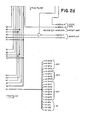
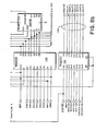
- FIG. 2 is a block diagram of a specific arrangement of a processor interface circuit in accordance with the invention and comprises an address decoder and associated selection circuitry for the selection and control of various elements of the Electronic Postage Meter. It will be appreciated that the circuit arrangement herein described is preferably embodied in a custom LSI microchip, however, it will be understood that the use of conventional logic components is also contemplated.
- the demultiplexer 12 in conventional manner demultiplexes the address/data bus 14 of a microprocessor (not shown in FIG. 2), suitably an 8085 series microprocessor available from the Intel Corporation or an NSC800 series microprocessor available from the National Semiconductor Corporation.
- the bus 14 communicates with the demultiplexer 12 on communication lines 16 through a conventional transceiver circuit arrangement 18.
- ADDRESS LATCH ENABLE (ALE) signal 20 from the microprocessor is "anded" with the microprocessor read strobe signal 22 to provide the latching signal for latching the address information for the demultiplexer 12.
- ALE ADDRESS LATCH ENABLE
- the demultiplexed address information is fed out on lines 24 for use in other parts of the EPM and are internally connected at 26 to the decoder section 28.
- the high order address signals directly from the microprocessor are communicated on lines 30 to the decoder section 28.
- An .external decode signal, EXTDEC, is also input to the decoder section 28.
- the decoder section 28 receives and decodes a complete input address received at 26 and 30 to provide select outputs for the various parts of the system.
- the low order demultiplexed address lines A ⁇ , Al and A2 are utilized as inputs to control flip-flops 32 along with the microprocessor write strobe WR received at 34 from the microprocessor.
- the control flip-flop section generates four control signals in response to these inputs in addition to a decoder reset signal and other derived signals, i.e. EXT-INTP, a pulse signal generated at the activation of the illegal memory access output pin, and a select signal CONTRAL-s for the selection of the Control Flip Flop block.
- NVM output control block 36 Outputs from the decoder 28 are provided to NVM output control block 36.
- This control block 36 in accordance with the invention provides a fail-safe NVM device selection. The selection of either NVM is disabled if the NVM write line is shorted to the "active" state. The NVM write strobe is disabled whenever the other devices are selected or in the event that both NVMs are simultaneously selected.
- an illegal address control block 38 in conjunction with the decoder 28 detects when the microprocessor read or write strobes attempt to access addresses an illegal, i.e. unused, memory space and, as discussed below, provides a signal output for interrupting the processor.
- Status and control block 40 monitors the outputs from the control Flip-Flop section and provides a control port to generate a decoder reset and to control the selection of an internal or external communication through an "Echoplex" I/O section 42.
- the section also includes an 8-bit timer to set the Transmit Baud rate for the serial communications.
- Dual Timer section 44 provides two programmable 16-bit timers.
- the system clock is the clock input to the timers.
- each is programmable for continuous or for one-shot operation for generating an interrupt when the programmed count is completed.
- an 8-bit counter divider can be selected to prescale the clock input or the ripple output of the first timer may be selected as the clock input to the second timer.
- serial I/O block 46 and parallel I/O block 48 are utilized for communication with a keyboard and display and for motor control, sensing postal value and miscellaneous control functions.
- an Interrupt Status and Control Block 50 is provided along with an interrupt mask control port for enabling selected interrupts to interrupt the systems processor.
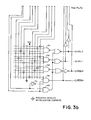
- FIG. 3 shows a schematic of an embodiment of a decoder block for providing a decoded memory map in accordance with the invention.
- the crossed lines with a circle superposed are used to indicate the preferred conductive path in a customized chip arrangement. It will be appreciated that the illustrated arrangement is extremely convenient in that the decoded memory map as described below may be modified easily with only a few mask changes.
- the various addresses communicated in known manner from the microprocessor and demultiplexer as described previously are each fed to leads Al through A15 of the decoder block 28.
- the address bits on address lines All through A15 are supplied to NAND gates 52, 54, 56, 58, and 60 and inverted at inverters 62, 64, 66, 68, and 70 and applied as illustrated to the NAND gates 52, 54, 56, and 58.
- An external decode signal 72 (see also FIG. 2) is applied to NAND gate 60.
- the output of NAND gate 60 is NOR'D with the outputs of gates 52, 54, and 56.
- the EXTDEC signal is also applied directed to gate 58. It will be noted that when "active" this signal will disable the decode function.
- the decoded outputs from the connections illustrated in FIG. 3 for the preferred embodiment are as.shown in Table I and in FIG. 4.
- an active DVOID output is provided from NAND gate 74 when none of the system's blocks are selected.
- the address bits when appropriately decoded as in the illustrated circuit by NAND gates 76, 78, 80, 82, 84, and 86 and inverters 88, 90, 92, 94, and 96 provide an "active" output IO whenever any of the I/O functions is selected and an "active" I/O read output whenever any of the internal circuit functional blocks are selected.
- Address bits A3 and A4 are applied to 2-to-4 demultiplexer 98 and decoded with other low order address bits for providing output signals as defined in Table I for selecting the appropriate blocks.
- the signal DVOID is not necessarily limited to its previously described function.
- a signal VINT from the control flip-flop block further described below may be used to convert this DVOID signal to another decode output.
- This signal shown as “ECHO/VOID” in FIG. 3 is available if the circuits internal ECHOPLEX block 42 is utilized.
- an external "echoplex” section that is, when the signal “EXTECHO” is “active” the “ECHO/VOID#” output becomes the “select” signal for the external block and the "select” signal for the internal echoplex section, "ECHO-S" is disabled.
- Control Flip-Flop section 32 As mentioned previously, the Control Flip-Flop section 32, more particularly shown in FIG. 5, generates four control output signals and their complements for controlling the generation of an illegal address interrupt signal to the processor, to provide an independent enable/disable for the access to two separate NVM storage devices, to enable and disable meter postage printing and access to nonvolatile storage.
- the low order address signals A0, Al, and A2 are fed to a 3-to-8 Line Decoder Multiplexer 102 equivalent to a 74HC138 available from RCA to set and reset flip-flops 104, 106, 108, and 110.
- the processor strobe signal WR and the select signal CNTRL-S are applied to the enable inputs of decoder 102. As illustrated, it is apparent that the control flip-flops are selectively controlled when both these signals are "active".
- the decoder reset signal RST and EXT-INTP (a pulse signal generated at the activation of the illegal memory access interrupt signal) are "NAND'D" at "NAND” gate 112, inverted at inverter and applied to each of the flip-flops 104 and 110.
- Table II shows the preferred decoded control signals in response to the appropriate addresses.
- the outputs from flip-flop 104 designated UNLOCK are preferably active to enable postage printing and for NVM access.
- the preset value is inactive to prevent printing and NVM access.
- the signal WRl-EN and WR2-EN are "active" for write access to respective NVM devices and #2. Again, for best results the preset values are "inactive”.
- the output VINT which as previously discussed is fed to the decoder section 28 is active to enable an interrupt generation whenever an illegal memory access is attempted. It will be appreciated that this is preferred since in the "inactive" state it may be used to reset the generated interrupt signal or to disable the interrupt so that it may be used as a spare decode output.
- the VINT preset signal is “active" to enable the interrupt.
- the illegal address control block 38 is shown more particularly in FIG. 6. This circuit is used to provide an indication of when access to unused memory space is attempted.
- the DVOID decoded signal output from the decoder section 28 is nanded at NAND gate 106 with the Q output from a D Flip-Flop 108:
- the processors read strobe RD and write strobe WR are NAND'D at NAND gate 110, inverted and applied to the clock input of the D flip-flop 108.
- the decoder reset signal is NANDED with the "VINT" signal from the control flip-flop section 32 at NAND gate 112 and applied to the RESET input shown as CLR in the Figure.
- the decoded void memory space indication will be latched at the lead edge of either the read or the write strobe of the microprocessor to provide the output INT-VOID from the Q terminal of flip-flop 108.
- the INT-VOID signal is provided to the system microprocessor as an interrupt signal. Preferably this indication will remain latched until reset by the reset signal from the microprocessor.
- the output is inverted at inverter 116 and supplied at 118 at INT-VOID.
- this INT-VOID output pin in open-drain so as to permit any of a number of open-drain outputs wire-ored to this pin to activate the output signal.
- This output pin is then suitably tapped as the input signal EXT-INT which is furnished to the Status and Control Block. There, this signal is provided as a status port bit and upon its actuation, a 1 clock period pulse is generated on signal EXT-INTP.
- This EXT-INTP- is provided from the status and control section to reset the control flip-flop and parallel I/O sections to their default (safe) states when the INT-VOID output pin is activated.
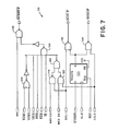
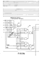
- FIG. 7 the NVM Output Control Block 36 is shown in greater detail.
- the WRITE access to the two independent NVM devices is independently enabled and disabled under software control.
- the NVM OUTPUT CONTROL will block the microprocessor write strobe WR unless either of the NVM decoded select signals SELl and SEL2 is available and the appropriate write enable signal from the control flip-flops are available at NAND gates 118 and 120.
- the output of these gates are inputs to NAND gate 122 whose output is applied to NAND gate 124. The output of this gate is inverted and supplied to NAND gate 126.
- the other signals applied to NAND gate 124 are the decoded select signals NVM1, NVM2, ROM, RAM and VOID are taken from the output drivers and applied to NAND gate 124, with NVM 1 and NVM2 being NOR'D at NOR gate 128 and inverted before being applied to 124. It will be appreciated that the write strobe WR is blocked if the appropriate memory space is not selected. It will also be appreciated that if both NVMs are selected simultaneously the write strobe will also be blocked.
- a further protection feature is provided in the event that the NVM write strobe output is shorted "active".
- the address enable strobe at 20 is applied as the clock signal to a D flip-flop 130. If the NVMWR is shorted active, the ALE signal clocks the Q output low to block both of the NVM device selection signals at NAND gates 132 and 134.
- FIG. 8 is a schematic of the status and control block.
- the block comprises a status port to allow monitoring of the control flip-flop outputs.
- the outputs of the control flip-flop block 32 are applied to buffer 136 for output to data bus 138, see also FIG. 2.
- the system clock input from 140 (see FIG. 2) is used in conventional fashion for timing the internal reset output by counting through D flip-flops 142, 144, and 146 to provide signal IRST which is the control signal for resetting all of the flip-flops in the circuit and is applied along with the System Reset to AND gate 148, (see FIG. 2).
- the block select signal STAT-S for this block, the write strobe, read strobe, and lowest order address bit are decoded to clock the writing of data at octal flip-flop 150, for initiating a general decoder reset under the control of appropriate software commands and for setting a baud-rate divider circuit if desired.
- the EXTECHO signal from D flip-flop 152 is used as previously discussed for selection of an external communication device (not shown).
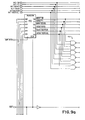
- the Interrupt Controller block 50 is shown in more detail in FIG. 9.
- the interrupt controller in accordance with the invention provides great flexibility in the servicing of the various interrupt signals to the microprocessor.
- Signal INTA from the system microprocessor is an interrupt acknowledge. It will be appreciated that if the INTA line is held or tied in the "inactive" state, each interrupt signal input applied through gates indicated generally at 156 and fed to NAND gate 158 will create an interrupt request signal INTR for communication to the system's microprocessor.
- mask bits may be fed as data on data input bus 16 for providing masking bits to D -flip-flops 160 for latching.
- the latched outputs from 160 are applied to gates 156 so that the interrupt request will be generated whenever an unmasked device requests service. The particular device requesting service may be determined by reading the status buffer 154.
- the interrupt lines are also coded at the gates indicated generally at 162 for feeding to latch 164 which also provides similar information.
- a vectored interrupt for the handling of service requests.
- a non-masked interrupt results in the generation of an interrupt-request signal to the systems microprocessor.
- the microprocessor upon receiving this signal will transmit an interrupt acknowledge signal INTA.
- This signal places the contents of the opcode latch 166 onto the data bus.
- the processor "interprets this data as an opcode, normally a call instruction for the microprocessor.
- the microprocessor Upon execution of the instruction, the microprocessor generates another INTA pulse to enable the lower vector latch 168.
- the encoding of bits on this latch desirably reflects a predetermined code representing the highest priority interrupt.
- the next INTA pulse in response to the call of this OPCODE, will place the data residing in latch 170, preferably the upper vector address data, onto the data bus 138.
- the INTR-S signal is utilized to select this block.
- the low order address signals A ⁇ through A2 are used as illustrated to decode the various control signals on the gates indicated generally at 140.
- Echoplex circuits suitable for use in block 42 are discussed in U.S. Patent No. 4,301,507 incorporated by reference herein.
- Serial I/O and parallel I/O port circuits are well known and will not be discussed further herein.
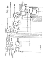
- FIG. 10 and FIG. 11 are timing diagrams showing the interrelationship of signals previously discussed. The designated parameters and preferred timing are shown in TABLE III. It is believed that these diagrams will be readily understood by those skilled in the art so they will not be further described except with regard to the operation of the circuit.
- the circuit 10 in accordance with the invention receives and decodes the-periodic address signals communicated from the microprocessor and received at decoder block 28 and control flip-flop block 32.
- the address signals are decoded to provide an "active" selection signal for each of the various blocks of the circuit 10 and the memory devices of the electronic postage meter depending upon the communication of the appropriate addresses for the particular device.
- the DVOID signal from the decoder block 28 goes “active” causing the output of gate 106 (FIG. 6) to go high and latching the Q output of flip-flop 108 active.
- a latched interrupt signal is sent to the interrupt control block 50 for communication to the microprocessor which responds as previously described above in conjunction with FIG. 9 whenever an illegal access is attempted.
- Protection is also provided during system power up with the use of the unlock control flip-flop signal. It is a master control of access to the NVM's and postage printing which will disable these functions until the software operating system is ready to enable them.
- the output from gate 126 is not shorted active and so to assure that writing to the NVM is being commanded by the microprocessor, the selection of a nonvolatile memory is blocked if NVMWR is held active.
- the output write enable signal NVMWR is fed to latch 130 (FIG. 7) which is clocked by the address-latch-enable signal (ALE) from the microprocessor.
- ALE address-latch-enable signal
- NVMWR is active when the ALE signal becomes active, the Q output of latch 130 goes high and blocks the output of gates 132 and 134.
- a nonvolatile memory there must be a periodically active nonvolatile memory write enabling signal and selection of only one nonvolatile memory to assure that the microprocessor is providing the appropriate data to the appropriately selected NVM.
Landscapes
- Physics & Mathematics (AREA)
- General Physics & Mathematics (AREA)
- Engineering & Computer Science (AREA)
- Mathematical Physics (AREA)
- Theoretical Computer Science (AREA)
- Storage Device Security (AREA)
- Devices For Checking Fares Or Tickets At Control Points (AREA)
- Techniques For Improving Reliability Of Storages (AREA)
Applications Claiming Priority (2)
| Application Number | Priority Date | Filing Date | Title |
|---|---|---|---|
| US710871 | 1985-03-12 | ||
| US06/710,871 US4710882A (en) | 1985-03-12 | 1985-03-12 | Electronic postage meter having a nonvolatile memory selection means |
Publications (3)
| Publication Number | Publication Date |
|---|---|
| EP0194658A2 true EP0194658A2 (fr) | 1986-09-17 |
| EP0194658A3 EP0194658A3 (en) | 1987-04-29 |
| EP0194658B1 EP0194658B1 (fr) | 1992-03-25 |
Family
ID=24855886
Family Applications (1)
| Application Number | Title | Priority Date | Filing Date |
|---|---|---|---|
| EP86103279A Expired EP0194658B1 (fr) | 1985-03-12 | 1986-03-12 | Machine d'affranchissement électronique ayant des moyens de sélection pour une mémoire non volatile |
Country Status (5)
| Country | Link |
|---|---|
| US (1) | US4710882A (fr) |
| EP (1) | EP0194658B1 (fr) |
| JP (1) | JPS61260378A (fr) |
| CA (1) | CA1247252A (fr) |
| DE (1) | DE3684495D1 (fr) |
Cited By (1)
| Publication number | Priority date | Publication date | Assignee | Title |
|---|---|---|---|---|
| US5996890A (en) * | 1997-01-29 | 1999-12-07 | Neopost Limited | Postage metering apparatus |
Families Citing this family (11)
| Publication number | Priority date | Publication date | Assignee | Title |
|---|---|---|---|---|
| FR2617997A1 (fr) * | 1987-07-07 | 1989-01-13 | Mitsubishi Electric Corp | Micro-ordinateur a memoire programmable, pour le controle du nombre des temps d'ecriture dans la memoire |
| US5012425A (en) * | 1988-12-30 | 1991-04-30 | Pitney Bowes Inc. | EPM having an improvement in non-volatile storage of accounting data |
| US5021963A (en) * | 1988-12-30 | 1991-06-04 | Pitney Bowes Inc. | EPM having an improvement in accounting update security |
| US5121327A (en) * | 1989-10-18 | 1992-06-09 | Pitney Bowes Inc. | Microcomputer-controlled electronic postage meter having print wheels set by separate d.c. motors |
| US5276844A (en) * | 1991-08-05 | 1994-01-04 | Ascom Autelca Ltd. | Protection system for critical memory information |
| US5438519A (en) * | 1993-02-10 | 1995-08-01 | Pitney Bowes Inc. | Electronic postage meter having memory write access second chance hard timer means |
| CA2137505C (fr) * | 1993-12-09 | 1999-05-04 | Young W. Lee | Circuit limiteur d'acces a un dispositif multi-memoire |
| US5377264A (en) * | 1993-12-09 | 1994-12-27 | Pitney Bowes Inc. | Memory access protection circuit with encryption key |
| US5530840A (en) * | 1993-12-09 | 1996-06-25 | Pitney Bowes Inc. | Address decoder with memory allocation for a micro-controller system |
| CA2137504C (fr) * | 1993-12-09 | 1998-08-25 | Young W. Lee | Circuit de surveillance pour detecter les acces non autorises a une memoire |
| MY135121A (en) | 2001-07-18 | 2008-02-29 | Shell Int Research | Wellbore system with annular seal member |
Family Cites Families (7)
| Publication number | Priority date | Publication date | Assignee | Title |
|---|---|---|---|---|
| US3938095A (en) * | 1971-11-04 | 1976-02-10 | Pitney-Bowes, Inc. | Computer responsive postage meter |
| US3978457A (en) * | 1974-12-23 | 1976-08-31 | Pitney-Bowes, Inc. | Microcomputerized electronic postage meter system |
| FR2486687B1 (fr) * | 1980-07-09 | 1986-08-22 | Roneo Alcatel Ltd | Compteur d'affranchissement postal |
| GB2101370A (en) * | 1981-06-26 | 1983-01-12 | Philips Electronic Associated | Digital data apparatus with memory interrogation |
| US4578774A (en) * | 1983-07-18 | 1986-03-25 | Pitney Bowes Inc. | System for limiting access to non-volatile memory in electronic postage meters |
| US4564922A (en) * | 1983-10-14 | 1986-01-14 | Pitney Bowes Inc. | Postage meter with power-failure resistant memory |
| US4573141A (en) * | 1984-04-12 | 1986-02-25 | General Electric Company | Memory interface for communicating between two storage media having incompatible data formats |
-
1985
- 1985-03-12 US US06/710,871 patent/US4710882A/en not_active Expired - Lifetime
-
1986
- 1986-03-11 CA CA000503779A patent/CA1247252A/fr not_active Expired
- 1986-03-12 EP EP86103279A patent/EP0194658B1/fr not_active Expired
- 1986-03-12 JP JP61054581A patent/JPS61260378A/ja active Pending
- 1986-03-12 DE DE8686103279T patent/DE3684495D1/de not_active Expired - Fee Related
Cited By (1)
| Publication number | Priority date | Publication date | Assignee | Title |
|---|---|---|---|---|
| US5996890A (en) * | 1997-01-29 | 1999-12-07 | Neopost Limited | Postage metering apparatus |
Also Published As
| Publication number | Publication date |
|---|---|
| EP0194658B1 (fr) | 1992-03-25 |
| EP0194658A3 (en) | 1987-04-29 |
| JPS61260378A (ja) | 1986-11-18 |
| DE3684495D1 (de) | 1992-04-30 |
| CA1247252A (fr) | 1988-12-20 |
| US4710882A (en) | 1987-12-01 |
Similar Documents
| Publication | Publication Date | Title |
|---|---|---|
| EP0181443B1 (fr) | Micro-ordinateur monopuce | |
| EP0099244B1 (fr) | Systèmes de multiprocesseurs fractionnables | |
| US4301507A (en) | Electronic postage meter having plural computing systems | |
| EP0194658B1 (fr) | Machine d'affranchissement électronique ayant des moyens de sélection pour une mémoire non volatile | |
| JP2597153B2 (ja) | 書込み保護装置 | |
| US5040178A (en) | Method of fault protection for a microcomputer system | |
| US4998203A (en) | Postage meter with a non-volatile memory security circuit | |
| EP0513880B1 (fr) | Systèmes à microprocesseur pour arrangements de machine à affranchir électronique | |
| EP0099571B1 (fr) | Boîte pour dispositif électronique tel qu'une machine à affranchir | |
| EP0712078B1 (fr) | Méthode et processeur de données à opération transparente dans un mode d'arrière-plan | |
| EP0197345B1 (fr) | Machine à affranchir électronique ayant un circuit de protection pour mise en circuit et pour coupure de l'alimentation | |
| CA1159574A (fr) | Systeme de traitement de donnees comprenant un dispositif d'adressage a registres internes | |
| EP0223130B2 (fr) | Circuit pour machine d'affranchissement électronique | |
| EP0194660B1 (fr) | Machine d'affranchissement possédant un décodeur de direction de routines mises en mémoire ainsi qu'un signal d'avertissement d'accès illégal à la mémoire | |
| EP0194661B1 (fr) | Circuit de retard pour la mise en circuit d'une machine à affranchir électronique | |
| US4916623A (en) | Electronic postage meter having redundant memory | |
| US4635223A (en) | Fail safe protection circuitry for a commerical microprocessor in encryption equipment | |
| JPS59112380A (ja) | 電子郵便料金計におけるフア−ムウエア分岐点を制御する方法及び装置 | |
| CA1250052A (fr) | Machine a affranchir electronique a decodeur de cartes memoire | |
| GB1577592A (en) | Data processing apparatus | |
| US5438519A (en) | Electronic postage meter having memory write access second chance hard timer means | |
| US4577283A (en) | Postage meter with keyboard keys for causing meter operations to be performed | |
| EP0356052B1 (fr) | Machine à affranchir | |
| EP0020972B1 (fr) | Dispositif microprocesseur commandé par programme | |
| EP0657853A2 (fr) | Décodeur d'adresse avec circuit d'état d'attente de mémoire |
Legal Events
| Date | Code | Title | Description |
|---|---|---|---|
| PUAI | Public reference made under article 153(3) epc to a published international application that has entered the european phase |
Free format text: ORIGINAL CODE: 0009012 |
|
| AK | Designated contracting states |
Kind code of ref document: A2 Designated state(s): CH DE FR GB IT LI NL |
|
| PUAL | Search report despatched |
Free format text: ORIGINAL CODE: 0009013 |
|
| AK | Designated contracting states |
Kind code of ref document: A3 Designated state(s): CH DE FR GB IT LI NL |
|
| 17P | Request for examination filed |
Effective date: 19870904 |
|
| 17Q | First examination report despatched |
Effective date: 19901113 |
|
| GRAA | (expected) grant |
Free format text: ORIGINAL CODE: 0009210 |
|
| AK | Designated contracting states |
Kind code of ref document: B1 Designated state(s): CH DE FR GB IT LI NL |
|
| ITF | It: translation for a ep patent filed | ||
| REF | Corresponds to: |
Ref document number: 3684495 Country of ref document: DE Date of ref document: 19920430 |
|
| ET | Fr: translation filed | ||
| PLBE | No opposition filed within time limit |
Free format text: ORIGINAL CODE: 0009261 |
|
| STAA | Information on the status of an ep patent application or granted ep patent |
Free format text: STATUS: NO OPPOSITION FILED WITHIN TIME LIMIT |
|
| 26N | No opposition filed | ||
| REG | Reference to a national code |
Ref country code: GB Ref legal event code: IF02 |
|
| PGFP | Annual fee paid to national office [announced via postgrant information from national office to epo] |
Ref country code: NL Payment date: 20040216 Year of fee payment: 19 |
|
| PGFP | Annual fee paid to national office [announced via postgrant information from national office to epo] |
Ref country code: DE Payment date: 20040430 Year of fee payment: 19 |
|
| PGFP | Annual fee paid to national office [announced via postgrant information from national office to epo] |
Ref country code: GB Payment date: 20050309 Year of fee payment: 20 |
|
| PG25 | Lapsed in a contracting state [announced via postgrant information from national office to epo] |
Ref country code: IT Free format text: LAPSE BECAUSE OF NON-PAYMENT OF DUE FEES;WARNING: LAPSES OF ITALIAN PATENTS WITH EFFECTIVE DATE BEFORE 2007 MAY HAVE OCCURRED AT ANY TIME BEFORE 2007. THE CORRECT EFFECTIVE DATE MAY BE DIFFERENT FROM THE ONE RECORDED. Effective date: 20050312 |
|
| PGFP | Annual fee paid to national office [announced via postgrant information from national office to epo] |
Ref country code: FR Payment date: 20050321 Year of fee payment: 20 Ref country code: CH Payment date: 20050321 Year of fee payment: 20 |
|
| PG25 | Lapsed in a contracting state [announced via postgrant information from national office to epo] |
Ref country code: NL Free format text: LAPSE BECAUSE OF NON-PAYMENT OF DUE FEES Effective date: 20051001 Ref country code: DE Free format text: LAPSE BECAUSE OF NON-PAYMENT OF DUE FEES Effective date: 20051001 |
|
| NLV4 | Nl: lapsed or anulled due to non-payment of the annual fee |
Effective date: 20051001 |
|
| PG25 | Lapsed in a contracting state [announced via postgrant information from national office to epo] |
Ref country code: GB Free format text: LAPSE BECAUSE OF EXPIRATION OF PROTECTION Effective date: 20060311 |
|
| REG | Reference to a national code |
Ref country code: GB Ref legal event code: PE20 |
|
| REG | Reference to a national code |
Ref country code: CH Ref legal event code: PL |