EP0195358A2 - Circuit de contrôle de basse tension - Google Patents
Circuit de contrôle de basse tension Download PDFInfo
- Publication number
- EP0195358A2 EP0195358A2 EP86103284A EP86103284A EP0195358A2 EP 0195358 A2 EP0195358 A2 EP 0195358A2 EP 86103284 A EP86103284 A EP 86103284A EP 86103284 A EP86103284 A EP 86103284A EP 0195358 A2 EP0195358 A2 EP 0195358A2
- Authority
- EP
- European Patent Office
- Prior art keywords
- voltage
- output
- effect transistor
- field effect
- deactivating
- Prior art date
- Legal status (The legal status is an assumption and is not a legal conclusion. Google has not performed a legal analysis and makes no representation as to the accuracy of the status listed.)
- Granted
Links
Images

Classifications
-
- G—PHYSICS
- G05—CONTROLLING; REGULATING
- G05F—SYSTEMS FOR REGULATING ELECTRIC OR MAGNETIC VARIABLES
- G05F1/00—Automatic systems in which deviations of an electric quantity from one or more predetermined values are detected at the output of the system and fed back to a device within the system to restore the detected quantity to its predetermined value or values, i.e. retroactive systems
- G05F1/10—Regulating voltage or current
- G05F1/46—Regulating voltage or current wherein the variable actually regulated by the final control device is DC
- G05F1/56—Regulating voltage or current wherein the variable actually regulated by the final control device is DC using semiconductor devices in series with the load as final control devices
- G05F1/565—Regulating voltage or current wherein the variable actually regulated by the final control device is DC using semiconductor devices in series with the load as final control devices sensing a condition of the system or its load in addition to means responsive to deviations in the output of the system, e.g. current, voltage, power factor
- G05F1/569—Regulating voltage or current wherein the variable actually regulated by the final control device is DC using semiconductor devices in series with the load as final control devices sensing a condition of the system or its load in addition to means responsive to deviations in the output of the system, e.g. current, voltage, power factor for protection
- G05F1/571—Regulating voltage or current wherein the variable actually regulated by the final control device is DC using semiconductor devices in series with the load as final control devices sensing a condition of the system or its load in addition to means responsive to deviations in the output of the system, e.g. current, voltage, power factor for protection with overvoltage detector
-
- G—PHYSICS
- G06—COMPUTING OR CALCULATING; COUNTING
- G06F—ELECTRIC DIGITAL DATA PROCESSING
- G06F1/00—Details not covered by groups G06F3/00 - G06F13/00 and G06F21/00
- G06F1/26—Power supply means, e.g. regulation thereof
- G06F1/28—Supervision thereof, e.g. detecting power-supply failure by out of limits supervision
Definitions
- the present invention relates to low voltage control circuits, and more particularly to a low voltage control circuit for maintaining at least one output in a known state of the state of the inputs when at least one voltage to be monitored is above a threshold voltage and below a predetermined limit voltage.
- one or more microprocessors are employed with some form of non-volatile memory (NVM) capability to store critical postage accounting information.
- NVM non-volatile memory
- This information includes, for example, the amount of postage remaining in the meter for subsequent printing and the total amount of postage already printed by the meter.
- Other types of accounting or operating data may also be stored in the non-volatile memory, as desired.
- the microprocessor and other devices in the meter may be non-operational, unstable or function erratically until the voltages to be monitored, e.g., chip supply voltages, reach stable levels.
- Such erratic operation may result in the erasure of data or the writing of spurious data in NVM prior to reaching a known operational voltage during power-up and subsequent to falling below the known operational voltage during power-down of the meter.
- a low voltage control circuit and associated method for maintaining at least one output terminal in a known state regardless of the input state of the inputs when at least one voltage to be monitored is above a threshold voltage and below a predetermined limit voltage, comprising control means for providing a deactivating output voltage when the voltage to be monitored is below the predetermined limit voltage, output means electrically coupled to the control means for receiving the output voltage from the control means and for.
- the output means being deactivated in response to the deactivating output voltage to provide a known voltage state at the output terminal until the voltage to be monitored reaches the predetermined limit voltage whereupon the control means will provide an activate output voltage to the output means to enable the voltage state at the output terminal to be controlled by the state of the inputs.
- a low voltage control circuit in accordance with the present invention is indicated generally at 10.
- the low voltage control circuit 10 includes a control section indicated generally at 12, to the left of the dotted line in Fig. 1, and an output section indicated generally at 14 to the right of the dotted line in Fig. 1.
- the ground point is synonymous with the. negative output supply voltage V SS .
- the control section 12 includes a supply line 16 for receiving a voltage to be monitored V l , which may be a regulated or unregulated chip supply voltage.
- the supply line 16 is coupled to the cathode of a Zener diode 18.
- the anode of the Zener diode 18 is coupled to ground through biasing resistor 20.
- the anode of the Zener diode 18 is coupled to the gate terminal of a field effect transistor in the form of an N-channel MOSFET 22.
- the source terminal of the MOSFET 22 is grounded and the drain terminal is coupled to the input line through biasing resistor 24.
- the drain terminal of the MOSFET 22 is also coupled to the gate terminal of a field effect transistor in the form of a P-channel MOSFET 26.
- the source terminal of the MOSFET 26 is coupled to the positive output supply voltage and resistor 24.
- the drain terminal of the MOSFET 26 is coupled to a grounded biasing resistor 28 and to output point 30 over line 32.
- the output point 30 is coupled to the gate terminal of a field effect transistor in the form of an N-channel MOSFET 34 which has its source terminal coupled to the positive output supply voltage V DD , to be monitored V I .
- the drain terminal of the MOSFET 34 is coupled to the source terminal of a field f effect transistor in the form of a P-channel MOSFET 36, which is part of the output section 14. Additionally, the supply voltage V l is supplied directly to the source terminal of a field effect transistor in the form of a P-channel MOSFET 38 over line 40.
- the output point 30 is also coupled to the gate terminal of a first field effect transistor in the form of an N-channel MOSFET 42 and the gate terminal of a second field effect transistor in the form of a P-channel MOSFET 44, both of which form part of a first output portion of the output section 14, as indicated generally by the number 43.
- the output point 30 is similarly coupled to any subsequent output portions of the output section 14. As illustrated in Fig. 1, there are two subsequent output portions, the first of which is designated 45 and includes a first field effect transistor in the form of an N-channel MOSFET 46 and a second field effect transistor in the form of a P-channel MOSFET 48, each having their gate terminals coupled to the output point 30.
- Th second subsequent output portion designated 49 also includes a first field effect transistor in the form of an N - channel MOSFET 50 and a second field effect transistor in the form of a P-channel MOSFET 52 each having their gate terminals coupled to the output point 30.
- the output point 30 is also coupled to the gate terminal of a field effect transistor in the form of an N-channel MOSFET 54.
- the source terminal of the MOSFET 54 is ground or the negative output supply voltage, V SS ; and the drain terminal is coupled to the source terminal of a field effect transistor in the form of an N-channel MOSFET 56 in the third output portion 49.
- the source terminal of the MOSFET 42 is coupled to a first input line 58 to receive an Input and the drain terminal is coupled to the drain terminal of MOSFET 44.
- the source terminal of the MOSFET 44 is coupled to the output positive supply voltage V DD and to one end of a biasing resistor 60.
- the other end of the resistor 60 is coupled to the drain terminals of MOSFETs 42 and 44 and to the gate terminal of MOSFET 36 and the gate terminal of a field effect transistor in the form of an N-channel MOSFET 62 arranged in a push-pull configuration.
- the drain terminals of MOSFETs 36 and 62 are coupled together and the source terminal of MOSFET 62 grounded.
- a first output is obtained from an output line 64 which is coupled to the drain terminals of the MOSFETs 36. and 62.
- the source terminal of the MOSFET 46 is coupled to a second input line 66 to receive an Input and its .( drain terminal is coupled to the drain terminal of MOSFET 48.
- the source terminal of the MOSFET 48 is coupled to the output positive supply voltage, V DD , and to one end of a biasing resistor 68.
- the other end of the resistor 68 is coupled to the drain terminals of MOSFETs 46 and 48 and to the gate terminal of a field effect transistor in the form of an N-channel MOSFET 70 whose source terminal is grounded and whose drain terminal is coupled to an output line 72.
- the second output is obtained from output line 72.
- the source terminal of the MOSFET 50 is coupled to a third input line 74 to receive an Input and the drain terminal to the drain terminal of MOSFET 52.
- the source terminal of the MOSFET 52 is grounded.
- a biasing resistor 76 couples the source terminals of MOSFFTs 50 and 52 to ground.
- the drain terminals of the MOSFETs 50 and 52 are coupled to the gate terminals of MOSFET 38 and MOSFET.56 arranged in a push-pull configuration.
- the drain terminals of MOSFETs 38 and 56 are coupled together and the source terminal of MOSFET 56 is coupled to the drain terminal of MOSFET 54.
- the third output is obtained from an output line 78 coupled to the drain terminals of the MOSFETs 38 and .56.
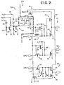
- FIG. 2 an alternative embodiment of a low voltage control circuit in accordance with the present invention which is illustrated as monitoring more than one voltage, here V 1 and V 2 , is indicated generally at 10A.
- V 1 and V 2 the same components which appear in Fig. 1 are given like numbers.
- the output section 14 includes the same components electrically connected in the same manner as previously described with reference to Fig. 1, there is no need to repeat a description of the output section 14 of Fig. 2.
- control section 12A of Fig. 2 has been modified from that shown in Fig. 1 to monitor a plurality of voltages, here V 1 and V 2 , although it should be understood that additional voltages may be monitored by further modifying the control section 12 of Fig. 1 in the same manner that it was modified to provide the control section 12A of Fig. 2.
- the supply voltage V 1 is applied to line 90 which is coupled to the cathode of Zener diode 18.
- the anode of the Zener diode 18 is coupled to ground through a biasing resistor 20.
- the anode of the Zener diode 18 in the form of an N-channel MOSFET 22 is grounded and the drain terminal is coupled to the positive output supply voltage V DD through biasing resistor 24.
- the input line 92 receives the second supply voltage V 2 .
- the drain terminal of the MOSFET 22 is also coupled to the gate terminal of a field effect transistor in the form of a P-channel MOSFET 26.
- the source terminal of the MOSFET 26 is coupled to the positive output supply voltage and the drain terminal is coupled to the source terminal of a field effect transistor in the form of a P-channel MOSFET 94.
- the drain terminal of the MOSFET 94 is coupled to the output point 30 through line 32 and to a grounded biasing resistor 28.
- a second Zener diode 96 has its cathode coupled to the line 92 and its anode coupled to grounded biasing resistor 98. Additionally, the anode of the Zener diode 96 is coupled to the gate of a field effect transistor in the form of an N- - channel MOSFET 100 whose source terminal is grounded and whose drain terminal is coupled to the positive output supply voltage V DD through biasing resistor 102 and to the gate terminal of the MOSFET 94.
- the voltage of the Zener diode 18 provides the setpoint for the maximum or limiting value of the voltage V l which corresponds to a stable operating voltage, such as a chip supply voltage, e.g. approximately 5V.
- a stable operating voltage such as a chip supply voltage, e.g. approximately 5V.
- the Zener diode 18 does not conduct until its breakdown voltage is reached.
- no voltage is applied to the gate terminal of the MOSFET 22 and its source terminal is grounded so that MOSFET 22 is OFF.
- This causes the gate terminal of the MOSFET 26 to be pulled high through biasing resistor 24, turning the MOSFET 26 off.
- the output at the output point 30 is low, being pulled toward ground by the biasing resistor 28.
- the low output voltage present at the output point 30 pulls the gate terminal of the MOSFET 34 low, turning MOSFE T 34 off.
- the positive output supply voltage is applied directly to the source terminal of the MOSFET 38 in the third output portion 49.
- the low output voltage present at the output point 30 is also applied to the gate terminals of the MOSFETs 42 and 44 causing the MOSFET 44 to turn ON and causing the MOSFET 42 to turn off.
- MOSFET 42 effectively provides an open circuit to the first input line 58 preventing the transmission of the Input voltage on line 58 to the output line 64.
- MOSFET 44 The positive voltage at the drain terminal of the MOSFET 44 as a result of its conduction is applied to the gate terminals of the MOSFETs 36 and 62, causing MOSFET 36 to turn off and MOSFET 62 to turn on when V 1 is above the threshold voltage of MOSFET 62.
- MO S FET 62 With MO S FET 62 conducting, its drain terminal and therefore the output line 64 are pulled toward ground providing a SAFE LOW PUSH-PULL OUTPUT on line 64 regardless of the magnitude or state of the input voltage present on input line 58.. Additionally, MOSFET 34 being off prevents the possibility of the positive output supply voltage from reaching the output 64.
- MOSFET 48 effectively provides an open circuit to the second input line 66 preventing the transmission of the Input voltage on line 66 to the output line 72.
- the positive voltage present at the drain terminal of the MOSFET 48 is applied to the gate terminal of the MOSFET 70, turning it on. With the MOSFET 70 on, its drain terminal and therefore output line 72, are pulled toward ground providing a second SAFE LOW OPEN-DRAIN OUTPUT on output line of the magnitude or state of the input voltage present on line 66.
- the presence of the low voltage at output point 30 also causes the MOSFET 52 to turn on, pulling the drain terminal of the MOSFET 52 toward ground, and MOSFET50 to turn off preventing the transmission of the Input voltage on input line 74 to the output line 78.
- MOSFET 38 With its gate terminal pulled low MOSFET 38 turns on, applying the positive output supply voltage V DD (high) to the output line 78.
- V DD positive output supply voltage
- a SAFE HIGH PUSH-PULL OUTPUT is provided on output line 78.
- the low voltage present at the gate terminals of MOSFET 56 and MOSFET 54 turns them off, providing a double level of protection for isolating ground, or V SS , from output 78.
- a high output present at output point 30 turns MOSFET 34 on to provide a high output at the source terminal of the MOSFET 36. Further, the high output present at the output point 30 turns MOSFET 42 on and MOSFET 44 off.
- the Input present on input line 58 is applied to the gate terminals of the MOSFETs 36 and 62. If the Input on input turning it off. However, the presence of a low voltage at the gate terminal of the MOSFET 36 causes it to turn on, transmitting a high output in the form of V DD to the output line 64. In contrast, if the Input on input line 58 is high, the gate terminal of the MOSFET 36 is biased high, turning it off. However, the presence of a high output at the gate terminal of the MOSFET 62 causes it to turn on, pulling the output line 64 toward ground to provide a low output on output line 64. Thus, the first output portion 43 of the output section 14 functions as an inverter.
- the MOSFET 46 when a high output is present at the output point 30, the MOSFET 46 is turned on and MOSFET 48 is turned off.
- the Input present on input line 66 is applied to the gate terminal of the MOSFET 70. If the Input on input line 66 is low, the gate terminal of MOSFET 70 is biased low and the MOSFET 70 is off, providing a high impedance output. If the Input on input line 66 is high, the gate terminal of the MOSFET 70 is biased high, causing MOSFET 70 to turn on and pulling it drain terminal and output line 72 toward ground to provide a low output on output line 72.
- the second output portion 45 of the output section 14 functions as an inverter with an open drain output,.
- the high output at point 30 turns on MOSFET 54, enabling the low output supply voltage to reach the output buffer MOSFET 56.
- a high output present at the output point 30 also turns MOSFET 50 on and turns MOSFET 52 off. If the Input on input line 74 is low, the gate terminal of the MOSFET 38 is biased low turning the MOSFET 38 on and the gate terminal of the MOSFET 56 is biased low turning the MOSFET 56 off Tbus the output line 78 receives a high voltage in the form of V I from M O S F ET 38. In contrast, if the Input on input line 74 is high, the gate terminal of the MOSFET 38 is biased high, turning the MOSFET 38 off. The presence of the high output at the gate terminal of the MOSFET 56 causes it to turn on, pulling the output line 78 toward ground to provide a low output on output line 78. Thus, the third output portion 49 of the output section 14 also functions as an inverter.
- V I and V 2 increase to the predetermined limit voltages, i.e., the set points of the Zener diodes 18 and 96
- the output at the output point 30 will be high.
- a high output in the form of V DD appears at the output point 30.
- the outpoint point 30 will remain low since both MOSFETs 26 and 94 are not conducting.
- output point 30 is pulled low through the current limiting resistor 28.
- V I or V 2 may be one in the same as V DD .
- the integrated circuit components of the low voltage control circuit described herein may be replaced by discrete components to provide a discrete low voltage control system.
- the voltage limiting devices, i.e., the Zener diodes may be replaced by integrated circuit components, e.g., a plurality of series connected MOSFETs.
Landscapes
- Engineering & Computer Science (AREA)
- Physics & Mathematics (AREA)
- General Physics & Mathematics (AREA)
- Theoretical Computer Science (AREA)
- General Engineering & Computer Science (AREA)
- Electromagnetism (AREA)
- Radar, Positioning & Navigation (AREA)
- Automation & Control Theory (AREA)
- Electronic Switches (AREA)
- Control Of Electrical Variables (AREA)
Applications Claiming Priority (2)
| Application Number | Priority Date | Filing Date | Title |
|---|---|---|---|
| US710798 | 1985-03-12 | ||
| US06/710,798 US4746818A (en) | 1985-03-12 | 1985-03-12 | Circuit for maintaining the state of an output despite changes in the state of input |
Publications (3)
| Publication Number | Publication Date |
|---|---|
| EP0195358A2 true EP0195358A2 (fr) | 1986-09-24 |
| EP0195358A3 EP0195358A3 (en) | 1989-06-07 |
| EP0195358B1 EP0195358B1 (fr) | 1994-07-27 |
Family
ID=24855585
Family Applications (1)
| Application Number | Title | Priority Date | Filing Date |
|---|---|---|---|
| EP86103284A Expired - Lifetime EP0195358B1 (fr) | 1985-03-12 | 1986-03-12 | Circuit de contrôle de basse tension |
Country Status (5)
| Country | Link |
|---|---|
| US (1) | US4746818A (fr) |
| EP (1) | EP0195358B1 (fr) |
| JP (1) | JPS61257016A (fr) |
| CA (1) | CA1296057C (fr) |
| DE (1) | DE3689986T2 (fr) |
Cited By (2)
| Publication number | Priority date | Publication date | Assignee | Title |
|---|---|---|---|---|
| FR2699755A1 (fr) * | 1992-12-22 | 1994-06-24 | Sgs Thomson Microelectronics | Circuit de démarrage et de sécurité contre les coupures d'alimentation, pour circuit intégré. |
| WO2010089544A1 (fr) * | 2009-02-04 | 2010-08-12 | Novacta Biosystems Limited | Dérivés d'actagardine |
Families Citing this family (14)
| Publication number | Priority date | Publication date | Assignee | Title |
|---|---|---|---|---|
| US4998203A (en) * | 1985-03-12 | 1991-03-05 | Digiulio Peter C | Postage meter with a non-volatile memory security circuit |
| US5107507A (en) * | 1988-05-26 | 1992-04-21 | International Business Machines | Bidirectional buffer with latch and parity capability |
| US5173619A (en) * | 1988-05-26 | 1992-12-22 | International Business Machines Corporation | Bidirectional buffer with latch and parity capability |
| US5121327A (en) * | 1989-10-18 | 1992-06-09 | Pitney Bowes Inc. | Microcomputer-controlled electronic postage meter having print wheels set by separate d.c. motors |
| US5019720A (en) * | 1990-03-12 | 1991-05-28 | Ncr Corporation | Integrated circuit driver for serial bus having output overvoltage protection |
| US5132564A (en) * | 1990-07-27 | 1992-07-21 | North American Philips Corp. | Bus driver circuit with low on-chip dissipation and/or pre-biasing of output terminal during live insertion |
| US5894176A (en) * | 1991-06-14 | 1999-04-13 | Integrated Device Technology, Inc. | Flexible reset scheme supporting normal system operation, test and emulation modes |
| FR2674633B1 (fr) * | 1991-03-28 | 1995-06-23 | Sgs Thomson Microelectronics | Circuit de detection d'un seuil haut d'une tension d'alimentation. |
| US5634000A (en) * | 1991-07-31 | 1997-05-27 | Ascom Autelca Ag | Power-fail return loop |
| US5276844A (en) * | 1991-08-05 | 1994-01-04 | Ascom Autelca Ltd. | Protection system for critical memory information |
| US5500611A (en) * | 1994-09-30 | 1996-03-19 | Cirrus Logic, Inc. | Integrated circuit with input/output pad having pullup or pulldown |
| US5712542A (en) * | 1995-05-25 | 1998-01-27 | Ascom Hasler Mailing Systems Ag | Postage meter with improved handling of power failure |
| US5633603A (en) * | 1995-12-26 | 1997-05-27 | Hyundai Electronics Industries Co., Ltd. | Data output buffer using pass transistors biased with a reference voltage and a precharged data input |
| US5941987A (en) * | 1996-12-24 | 1999-08-24 | Intel Corporation | Reference cell for integrated circuit security |
Family Cites Families (7)
| Publication number | Priority date | Publication date | Assignee | Title |
|---|---|---|---|---|
| JPS56122132U (fr) * | 1980-02-18 | 1981-09-17 | ||
| US4380709A (en) * | 1980-05-15 | 1983-04-19 | Motorola, Inc. | Switched-supply three-state circuit |
| JPS5856286B2 (ja) * | 1980-12-25 | 1983-12-14 | 富士通株式会社 | 出力バッファ回路 |
| US4425517A (en) * | 1981-03-31 | 1984-01-10 | Rca Corporation | Fail soft tri-state logic circuit |
| JPS5894233A (ja) * | 1981-11-30 | 1983-06-04 | Fujitsu Ltd | Ttl論理回路 |
| US4446381A (en) * | 1982-04-22 | 1984-05-01 | Zilog, Inc. | Circuit and technique for initializing the state of bistable elements in an integrated electronic circuit |
| JPS6110319A (ja) * | 1984-05-30 | 1986-01-17 | Fujitsu Ltd | 出力制御回路 |
-
1985
- 1985-03-12 US US06/710,798 patent/US4746818A/en not_active Expired - Lifetime
-
1986
- 1986-03-11 CA CA000503784A patent/CA1296057C/fr not_active Expired - Fee Related
- 1986-03-12 DE DE3689986T patent/DE3689986T2/de not_active Expired - Fee Related
- 1986-03-12 EP EP86103284A patent/EP0195358B1/fr not_active Expired - Lifetime
- 1986-03-12 JP JP61054564A patent/JPS61257016A/ja active Pending
Cited By (5)
| Publication number | Priority date | Publication date | Assignee | Title |
|---|---|---|---|---|
| FR2699755A1 (fr) * | 1992-12-22 | 1994-06-24 | Sgs Thomson Microelectronics | Circuit de démarrage et de sécurité contre les coupures d'alimentation, pour circuit intégré. |
| EP0604270A1 (fr) * | 1992-12-22 | 1994-06-29 | STMicroelectronics S.A. | Circuit de démarrage et de sécurité contre les coupures d'alimentation pour circuit intégré |
| WO2010089544A1 (fr) * | 2009-02-04 | 2010-08-12 | Novacta Biosystems Limited | Dérivés d'actagardine |
| US8729031B2 (en) | 2009-02-04 | 2014-05-20 | Novacta Biosystems Limited | Compounds |
| EA020733B1 (ru) * | 2009-02-04 | 2015-01-30 | Новакта Биосистемс Лимитед | Производные актагардина |
Also Published As
| Publication number | Publication date |
|---|---|
| CA1296057C (fr) | 1992-02-18 |
| DE3689986T2 (de) | 1995-01-12 |
| US4746818A (en) | 1988-05-24 |
| EP0195358A3 (en) | 1989-06-07 |
| JPS61257016A (ja) | 1986-11-14 |
| EP0195358B1 (fr) | 1994-07-27 |
| DE3689986D1 (de) | 1994-09-01 |
Similar Documents
| Publication | Publication Date | Title |
|---|---|---|
| EP0195358A2 (fr) | Circuit de contrôle de basse tension | |
| US6448812B1 (en) | Pull up/pull down logic for holding a defined value during power down mode | |
| JP3427436B2 (ja) | 駆動回路 | |
| US6879191B2 (en) | Voltage mismatch tolerant input/output buffer | |
| US7180330B2 (en) | Output circuit | |
| KR19990067849A (ko) | 허용 전압 출력 버퍼 | |
| US7835124B2 (en) | Short circuit and over-voltage protection for a data bus | |
| EP0357366B1 (fr) | Circuit à miroir de courant amélioré | |
| US20040113661A1 (en) | Two-level supply voltage detection circuit | |
| US6344958B1 (en) | Overvoltage protection circuit with overvoltage removal sensing | |
| EP0704973A2 (fr) | Dispositif et méthode pour la protection d'un circuit électrique | |
| KR890005231B1 (ko) | 초기 스파이크 잡음 제거용 출력제어회로 | |
| EP0874462A1 (fr) | Circuit de tirage vers le haut et dispositif semi-conducteur en fasisant usage | |
| US5642059A (en) | Bus driver circuit with overvoltage protection | |
| EP0704974A1 (fr) | Circuit d'attaque de sortie de puce | |
| WO1995006357A1 (fr) | Circuits d'interface entre des dispositifs dont on a coupe l'alimentation et un bus | |
| JPH07129538A (ja) | 半導体集積回路 | |
| US6034448A (en) | Semiconductor switch | |
| EP0305482B1 (fr) | Circuit de terminaison d'une ligne de transmission de faible bruit | |
| JP3272809B2 (ja) | 半導体集積回路装置 | |
| JP2560380B2 (ja) | 出力過電流制限回路 | |
| EP0472797B1 (fr) | Circuit de protection contre la surcharge | |
| JP3704094B2 (ja) | リセット信号発生回路 | |
| KR920004332Y1 (ko) | 전원 출력단의 전압 보호회로 | |
| JP3295833B2 (ja) | 電源冗長システム |
Legal Events
| Date | Code | Title | Description |
|---|---|---|---|
| PUAI | Public reference made under article 153(3) epc to a published international application that has entered the european phase |
Free format text: ORIGINAL CODE: 0009012 |
|
| AK | Designated contracting states |
Kind code of ref document: A2 Designated state(s): CH DE FR GB LI |
|
| PUAL | Search report despatched |
Free format text: ORIGINAL CODE: 0009013 |
|
| RHK1 | Main classification (correction) |
Ipc: H03K 17/22 |
|
| AK | Designated contracting states |
Kind code of ref document: A3 Designated state(s): CH DE FR GB LI |
|
| 17P | Request for examination filed |
Effective date: 19891107 |
|
| 17Q | First examination report despatched |
Effective date: 19900731 |
|
| GRAA | (expected) grant |
Free format text: ORIGINAL CODE: 0009210 |
|
| AK | Designated contracting states |
Kind code of ref document: B1 Designated state(s): CH DE FR GB LI |
|
| REF | Corresponds to: |
Ref document number: 3689986 Country of ref document: DE Date of ref document: 19940901 |
|
| ET | Fr: translation filed | ||
| PLBE | No opposition filed within time limit |
Free format text: ORIGINAL CODE: 0009261 |
|
| STAA | Information on the status of an ep patent application or granted ep patent |
Free format text: STATUS: NO OPPOSITION FILED WITHIN TIME LIMIT |
|
| 26N | No opposition filed | ||
| REG | Reference to a national code |
Ref country code: GB Ref legal event code: IF02 |
|
| PGFP | Annual fee paid to national office [announced via postgrant information from national office to epo] |
Ref country code: GB Payment date: 20040303 Year of fee payment: 19 |
|
| PGFP | Annual fee paid to national office [announced via postgrant information from national office to epo] |
Ref country code: FR Payment date: 20040318 Year of fee payment: 19 |
|
| PGFP | Annual fee paid to national office [announced via postgrant information from national office to epo] |
Ref country code: CH Payment date: 20040322 Year of fee payment: 19 |
|
| PGFP | Annual fee paid to national office [announced via postgrant information from national office to epo] |
Ref country code: DE Payment date: 20040430 Year of fee payment: 19 |
|
| PG25 | Lapsed in a contracting state [announced via postgrant information from national office to epo] |
Ref country code: GB Free format text: LAPSE BECAUSE OF NON-PAYMENT OF DUE FEES Effective date: 20050312 |
|
| PG25 | Lapsed in a contracting state [announced via postgrant information from national office to epo] |
Ref country code: LI Free format text: LAPSE BECAUSE OF NON-PAYMENT OF DUE FEES Effective date: 20050331 Ref country code: CH Free format text: LAPSE BECAUSE OF NON-PAYMENT OF DUE FEES Effective date: 20050331 |
|
| PG25 | Lapsed in a contracting state [announced via postgrant information from national office to epo] |
Ref country code: DE Free format text: LAPSE BECAUSE OF NON-PAYMENT OF DUE FEES Effective date: 20051001 |
|
| REG | Reference to a national code |
Ref country code: CH Ref legal event code: PL |
|
| GBPC | Gb: european patent ceased through non-payment of renewal fee |
Effective date: 20050312 |
|
| PG25 | Lapsed in a contracting state [announced via postgrant information from national office to epo] |
Ref country code: FR Free format text: LAPSE BECAUSE OF NON-PAYMENT OF DUE FEES Effective date: 20051130 |
|
| REG | Reference to a national code |
Ref country code: FR Ref legal event code: ST Effective date: 20051130 |