EP0195467B1 - Dispositif de sondes à induction comprenant plusieurs sondes - Google Patents
Dispositif de sondes à induction comprenant plusieurs sondes Download PDFInfo
- Publication number
- EP0195467B1 EP0195467B1 EP86200232A EP86200232A EP0195467B1 EP 0195467 B1 EP0195467 B1 EP 0195467B1 EP 86200232 A EP86200232 A EP 86200232A EP 86200232 A EP86200232 A EP 86200232A EP 0195467 B1 EP0195467 B1 EP 0195467B1
- Authority
- EP
- European Patent Office
- Prior art keywords
- shielding
- arrangement
- probe
- electrode
- signal
- Prior art date
- Legal status (The legal status is an assumption and is not a legal conclusion. Google has not performed a legal analysis and makes no representation as to the accuracy of the status listed.)
- Expired - Lifetime
Links
- 239000000523 sample Substances 0.000 title claims description 62
- 230000006698 induction Effects 0.000 title claims 9
- 239000000758 substrate Substances 0.000 claims description 33
- 238000004519 manufacturing process Methods 0.000 claims description 5
- 238000009826 distribution Methods 0.000 claims description 4
- 238000000034 method Methods 0.000 claims description 3
- 238000000151 deposition Methods 0.000 claims 1
- 239000004020 conductor Substances 0.000 description 58
- 206010022000 influenza Diseases 0.000 description 11
- 239000000919 ceramic Substances 0.000 description 5
- PCHJSUWPFVWCPO-UHFFFAOYSA-N gold Chemical compound [Au] PCHJSUWPFVWCPO-UHFFFAOYSA-N 0.000 description 3
- 239000010931 gold Substances 0.000 description 3
- 229910052737 gold Inorganic materials 0.000 description 3
- 238000000206 photolithography Methods 0.000 description 3
- 230000003014 reinforcing effect Effects 0.000 description 3
- 239000000853 adhesive Substances 0.000 description 2
- 238000004026 adhesive bonding Methods 0.000 description 2
- 230000001070 adhesive effect Effects 0.000 description 2
- 230000005684 electric field Effects 0.000 description 2
- BUGBHKTXTAQXES-UHFFFAOYSA-N Selenium Chemical compound [Se] BUGBHKTXTAQXES-UHFFFAOYSA-N 0.000 description 1
- 239000012799 electrically-conductive coating Substances 0.000 description 1
- 239000011810 insulating material Substances 0.000 description 1
- 239000000463 material Substances 0.000 description 1
- 239000011224 oxide ceramic Substances 0.000 description 1
- 229910052574 oxide ceramic Inorganic materials 0.000 description 1
- TWNQGVIAIRXVLR-UHFFFAOYSA-N oxo(oxoalumanyloxy)alumane Chemical compound O=[Al]O[Al]=O TWNQGVIAIRXVLR-UHFFFAOYSA-N 0.000 description 1
- 230000002787 reinforcement Effects 0.000 description 1
- 229910052711 selenium Inorganic materials 0.000 description 1
- 239000011669 selenium Substances 0.000 description 1
- 238000007740 vapor deposition Methods 0.000 description 1
Images

Classifications
-
- G—PHYSICS
- G01—MEASURING; TESTING
- G01R—MEASURING ELECTRIC VARIABLES; MEASURING MAGNETIC VARIABLES
- G01R29/00—Arrangements for measuring or indicating electric quantities not covered by groups G01R19/00 - G01R27/00
- G01R29/24—Arrangements for measuring quantities of charge
-
- G—PHYSICS
- G01—MEASURING; TESTING
- G01R—MEASURING ELECTRIC VARIABLES; MEASURING MAGNETIC VARIABLES
- G01R1/00—Details of instruments or arrangements of the types included in groups G01R5/00 - G01R13/00 and G01R31/00
- G01R1/02—General constructional details
- G01R1/06—Measuring leads; Measuring probes
- G01R1/067—Measuring probes
- G01R1/06766—Input circuits therefor
Definitions
- the invention relates to an influenza probe arrangement according to the preamble of claim 1.
- an influenza probe arrangement is known from DE-A-2948660. Since the known influence probe arrangement is provided with several influence probes, the charge distribution on a charged surface can thus be determined more quickly than with the aid of only a single influence probe.
- the lines required in the known arrangement between the probe electrodes of the individual influenza probes and the associated high-resistance preamplifiers can, however, also absorb interference voltages in addition to the actual signal voltages, and it is very difficult to shield these lines against such interference voltages.
- a detector for an ink jet printer which responds to electrically charged ink droplets.
- This detector contains in one plane a probe electrode and a shielding electrode surrounding the probe electrode, which are connected to an amplifier via conductor tracks.
- the object of the present invention is to design an influenza probe arrangement of the type mentioned at the outset in such a way that the signal lines from the probe electrodes to the preamplifiers are better shielded against interference voltages. This object is achieved by the measures specified in claim 1.
- the signal conductor tracks run in the first level, i. H. in a center plane, and the shielding conductor tracks in parallel planes on the side faces of the preferably plate-shaped substrate arrangement, on the end faces of which the probe or shielding electrodes are located. In this way, the signal conductor track is shielded against external interference sources, but also against crosstalk from neighboring signal conductor tracks.
- the crosstalk from adjacent signal conductor tracks can be further reduced by arranging two further shield conductor tracks on both sides of a signal conductor track in the first level, which are connected to the same shielding electrode.
- the signal conductor tracks are connected to the input and the associated shielding conductor tracks are connected to the output of a voltage follower. This results in a homogeneous electric field when scanning the electrically charged surface between the shielding and the probe electrodes; on the other hand, the input capacity of the voltage follower is significantly reduced.
- the shielding electrode is surrounded on the end face by a further shielding electrode connected to ground.
- a method according to the invention for producing such an influenza probe arrangement provides that an electrically conductive coating is applied to the end face of a substrate arrangement provided with conductor tracks in three parallel planes in order to produce the shielding and probe electrodes, and that subsequently to form the probe and shielding electrodes which are electrically insulated from one another part of the covering is removed. It is preferably provided that for the manufacture of the substrate arrangement two electrically insulated plates are provided on each side with the shielding conductor tracks and that at least one of the two plates on the other side is at least provided with the signal conductor tracks and that the plates are then joined together in such a way that the side with the signal conductor tracks is in the middle. Both the probe and the shielding electrodes as well as the associated signal and shielding conductor tracks can be produced in this method by photolithography, which ensures economical production.
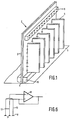
- Fig. 1 denotes a flat surface which is electrically charged.
- the flat surface can belong to an X-ray image sensor, e.g. B. a selenium plate, on which there is a charge pattern that corresponds to the intensity distribution of an X-ray image present in a previous exposure.
- This charge pattern is scanned by an influenza probe arrangement 2, which converts the charge into electrical signals at several points on the surface 1 at the same time.
- the speed at which the charge distribution on the surface 1 can be scanned - with the influence probe arrangement 2 and the surface 1 being shifted relative to one another - increases with the number of points whose charge is detected simultaneously.
- the influenza probe arrangement contains a plate-shaped substrate arrangement 3, the end face of which is parallel and at a short distance, for. B. 100 pm, from the surface to be scanned runs.
- the end face 4 is provided with probe electrodes, the potential of which corresponds to the charge density below these electrodes.
- the potentials of the individual electrodes are detected by high-resistance preamplifiers, which are located in hybrid amplifier modules 5 and which are connected to the associated probe electrodes via conductor tracks on the substrate arrangement 3.
- the output signals of the hybrid amplifier modules can be removed with a low impedance from a connector strip 6 and can be further processed there by suitable electronic circuits.
- the substrate arrangement 3 consists of two interconnected flat substrate plates.
- the substrate plates consist of a highly insulating, mechanically stable material, e.g. B. A1 2 0 3 and have a thickness of the order of 0.5 mm.
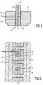
- probe electrodes 7 are arranged on the lower end face of the substrate plates 3 at regular intervals symmetrically to a first plane 6, the middle plane between the two substrate plates 3.
- the size of these probe electrodes determine the dimensions of the area whose charge is detected.
- a value of the probe electrode area suitable for reading out X-ray images is 150 x 150 ⁇ m.
- Each probe electrode 7 is enclosed by a shielding electrode 8, which is electrically insulated from the probe electrode by a narrow parting line 9.
- the shielding electrodes 8 are partly still on the end faces of the substrate arrangement 3, but partly also on the flat lower surfaces of reinforcing strips 10 which merge into the end faces and which are attached in the lower region of the substrate arrangement and likewise consist of insulating material. As will be explained in more detail below, they carry the same potential as the probe electrode enclosed by them, so that when the surface 1 is scanned, a practically homogeneous electric field is formed between it and the probe electrode.
- the shielding electrodes in turn are enclosed by an electrically conductive, grounded covering 11, which is separated from the shielding electrodes by a parting line 21 and which covers at least the lower surface of the reinforcing strip 10.
- each probe electrode 7 is connected to a signal conductor track 12, which is located in the central plane 6 of the substrate arrangement, i. H. located on the inner surface of one of the two substrate plates 3.
- Each shielding electrode is connected to a plurality of conductor tracks 13. These are located on the one hand on the outer surfaces of the substrate arrangement 3 and on the other hand also on the same inner surface as the signal conductor tracks. In this way, each signal conductor track is completely enclosed by several shielding conductor tracks (cf. FIG. 3).
- the shielding conductor tracks on the outer surfaces shield the signal conductor tracks in particular against interference coming from outside, while the shielding conductor tracks located in the central plane 6 prevent above all the crosstalk between adjacent signal conductor tracks.
- the covering 11 is connected to earth lines 14, which are guided on the outer surfaces of the substrate arrangement 3.
- FIG. 4 shows the signal and shielding conductor tracks on the inner surface of one of the two substrate plates, while in FIG. 5 the shielding conductor tracks and an earth conductor track are shown on the outer surface of the other substrate plate.
- the signal conductor tracks the upper end of which opens into a connecting eye 15, are guided in such a way that the connecting eyes of four signal conductor tracks each lie on a vertical straight line.
- Each signal conductor track 12 is surrounded by two shielding conductor tracks 13, which are connected to one another around the connection eyelet of the associated conductor track, the shielding conductor track being widened in this area and provided with a connection bore 16.
- the arrangement and the shape of the shielding conductor tracks belonging to the four signal conductor tracks on the outer surface can be seen from FIG. 5.
- each of these conductor tracks corresponds to the outer contour of two shielding conductor tracks 13 belonging to a signal conductor track 12 together with the widened area.
- the signal conductor tracks each have a circular recess 17, the diameter of which is larger than the diameter of the connection eyelets 15.
- there is also the earth conductor track 14 on the outer surface one for the influence probes on the substrate arrangement 3 in general Earth conductor track is sufficient, which expediently surrounds the amplifier modules (Fig. 1).
- the conductor tracks shown in FIGS. 4 and 5, each belonging to four probe electrodes and four shielding electrodes, continue periodically in the horizontal direction, so that the influence probe arrangement can carry an integral multiple of four influence probes.
- FIG. 6 schematically shows the connection of a probe electrode 7 and the shielding electrode 8 surrounding it to one of the amplifiers contained in a module 5.
- the amplifier is formed by an operational amplifier 18, the output of which is connected to the inverting input, so that an amplifier with a low-impedance output and voltage gain 1 (voltage follower) results.
- the shielding electrode 8 is connected via line 13 to the inverting input or to the low-resistance output of the amplifier, and the probe electrode 7 is connected via signal line 12 connected to the non-inverting input of the amplifier. Because of its voltage follower characteristic, the shielding electrode 8 assumes the same potential as the signal electrode 7, even if the charge density in the region of the shielding electrode differs significantly from that in the region of the signal electrode.
- the influenza probe assembly two aluminum oxide ceramic plates of the required size are first produced.
- the conductor tracks are then applied to the plates, preferably using photolithographic technology.
- the one printed circuit board is provided on both sides and the other plate on one side - but possibly also on both sides with an approximately 6 K thick gold layer - for example by vapor deposition.
- the shielding and earth conductor tracks are then etched out on the two ceramic plates according to FIG. 5 or in mirror image thereto by photolithography.
- the signal and shielding conductor tracks according to FIG. 4 are etched out on the still untreated gold layer of the one - and possibly also the other - ceramic plate.
- the two plates are then glued together using a suitable adhesive, after which the reinforcing strips 10 are connected to the ceramic plates, preferably also by gluing.
- the end face of the substrate arrangement created by gluing the ceramic plates together and the coincident surface of the reinforcement strips are then ground and polished until the conductor tracks become visible (under the microscope).
- a gold layer is deposited on the surface treated in this way, which is then in electrical contact with the signal, shielding and earth conductor tracks.
- the separating joints 9, 21 are then also etched into this layer by photolithography (FIG. 3), so that a grounded covering 11 and probe electrodes and shielding electrodes 7, 8 electrically insulated therefrom and from one another are formed, each of which is in contact with the associated conductor tracks .
- a hybrid amplifier module which contains four preamplifiers, is connected to eight contact pins each lying on a vertical straight line, as can be seen in FIG. 1.
- the hybrid amplifier modules 5 can be connected directly to the contact pins. However, it is more expedient to mount the hybrid amplifier modules 5 together with the connector strip 6 on a circuit board which is provided with conductor tracks for connecting the amplifier outputs to the connector strip 6 and with sockets for receiving the contact pins.
- probe electrodes are much denser or if the hybrid amplifier modules 5 are too large, these modules can also be fitted on both sides of the substrate arrangement.
- the substrate arrangement consists of two ceramic plates, the conductor tracks being guided in three planes to the end face thereof.
- the distance between two adjacent probe electrodes is always somewhat larger than the dimensions of a shielding electrode, so that only a relatively small number of probe electrodes can be present per unit length. This number can be increased by using more than two substrate plates, on the inner and outer surfaces of which the conductor tracks are attached, and when the probe electrodes are no longer arranged on a straight line, but offset against one another.
Landscapes
- Physics & Mathematics (AREA)
- General Physics & Mathematics (AREA)
- Measuring Leads Or Probes (AREA)
- Measurement Of Radiation (AREA)
- Testing Of Individual Semiconductor Devices (AREA)
Claims (8)
Applications Claiming Priority (2)
| Application Number | Priority Date | Filing Date | Title |
|---|---|---|---|
| DE3505615 | 1985-02-19 | ||
| DE19853505615 DE3505615A1 (de) | 1985-02-19 | 1985-02-19 | Influenzsondenanordnung mit mehreren influenzsonden |
Publications (2)
| Publication Number | Publication Date |
|---|---|
| EP0195467A1 EP0195467A1 (fr) | 1986-09-24 |
| EP0195467B1 true EP0195467B1 (fr) | 1990-01-03 |
Family
ID=6262870
Family Applications (1)
| Application Number | Title | Priority Date | Filing Date |
|---|---|---|---|
| EP86200232A Expired - Lifetime EP0195467B1 (fr) | 1985-02-19 | 1986-02-18 | Dispositif de sondes à induction comprenant plusieurs sondes |
Country Status (4)
| Country | Link |
|---|---|
| US (1) | US4760342A (fr) |
| EP (1) | EP0195467B1 (fr) |
| JP (1) | JPS61189466A (fr) |
| DE (2) | DE3505615A1 (fr) |
Families Citing this family (7)
| Publication number | Priority date | Publication date | Assignee | Title |
|---|---|---|---|---|
| US5070302A (en) * | 1989-09-05 | 1991-12-03 | Eastman Kodak Company | Capacitance probe for measuring a width of a clearance between parts |
| US5101159A (en) * | 1990-05-18 | 1992-03-31 | Trek, Inc. | Electrostatic pin hole detector |
| US5274336A (en) * | 1992-01-14 | 1993-12-28 | Hewlett-Packard Company | Capacitively-coupled test probe |
| GB2272976B (en) * | 1992-11-30 | 1996-06-05 | Stewart Hughes Ltd | A sensor |
| US6828767B2 (en) | 2002-03-20 | 2004-12-07 | Santronics, Inc. | Hand-held voltage detection probe |
| US20060192545A1 (en) * | 2005-02-28 | 2006-08-31 | Static Control Components, Inc. | Voltage detection pole |
| DE102010036409A1 (de) | 2010-07-15 | 2012-01-19 | Heinz-Gregor Johnen | Mobiler Personenlift |
Family Cites Families (7)
| Publication number | Priority date | Publication date | Assignee | Title |
|---|---|---|---|---|
| US3852768A (en) * | 1973-08-17 | 1974-12-03 | Ibm | Charge detection for ink jet printers |
| US4134137A (en) * | 1976-11-01 | 1979-01-09 | Xerox Corporation | Single wire microelectrometer imaging system |
| JPS55114962A (en) * | 1979-02-28 | 1980-09-04 | Ricoh Co Ltd | Surface potentiometer |
| DE2948660A1 (de) * | 1979-12-04 | 1981-06-11 | Philips Patentverwaltung Gmbh, 2000 Hamburg | Influenzsondenanordnung und verfahren zu ihrer herstellung |
| US4470009A (en) * | 1979-12-28 | 1984-09-04 | Canon Kabushiki Kaisha | Surface potentiometer |
| JPS5737270A (en) * | 1980-08-15 | 1982-03-01 | Canon Inc | Surface electrometer |
| JPS58144215U (ja) * | 1982-03-23 | 1983-09-28 | 岩崎通信機株式会社 | 変位計の静電容量プロ−プ |
-
1985
- 1985-02-19 DE DE19853505615 patent/DE3505615A1/de not_active Withdrawn
-
1986
- 1986-02-14 US US06/829,576 patent/US4760342A/en not_active Expired - Fee Related
- 1986-02-15 JP JP61029934A patent/JPS61189466A/ja active Pending
- 1986-02-18 EP EP86200232A patent/EP0195467B1/fr not_active Expired - Lifetime
- 1986-02-18 DE DE8686200232T patent/DE3668071D1/de not_active Expired - Lifetime
Also Published As
| Publication number | Publication date |
|---|---|
| US4760342A (en) | 1988-07-26 |
| DE3668071D1 (de) | 1990-02-08 |
| DE3505615A1 (de) | 1986-08-21 |
| JPS61189466A (ja) | 1986-08-23 |
| EP0195467A1 (fr) | 1986-09-24 |
Similar Documents
| Publication | Publication Date | Title |
|---|---|---|
| DE2524437C3 (de) | Schalttafelstruktur einer kapazitiv gekoppelten Tastatur | |
| DE3639367C2 (fr) | ||
| DE3885805T2 (de) | Filtereinheit für Verbinder. | |
| DE2542518C3 (fr) | ||
| DE3610821C2 (fr) | ||
| DE3824500A1 (de) | Elektrische kabelvorrichtung und damit ausgeruestete ladungssammelvorrichtung | |
| DE4407492A1 (de) | Einrichtung zur Abschirmung von auf einer Elektronikkarte angeordneten elektronischen Bauteilen gegen äußere, elektromagnetische Felder | |
| DE2525166A1 (de) | Kontakt-sondenvorrichtung | |
| DE2615354C2 (de) | Einrichtung zum Unterdrücken von statischer Elektrizität und Verfahren zum Herstellen derselben | |
| DE2703320A1 (de) | Troepfchenstrahlen-aufzeichnungsvorrichtung | |
| DE2752438A1 (de) | Anordnung fuer das packen von monolithisch integrierten halbleiterschaltungen | |
| DE3941029C2 (de) | Elektrostatischer Kapazitätsdetektor des Phasendiskriminierungstyps | |
| EP0403788A2 (fr) | Agencement de détecteur à bobines | |
| EP0195467B1 (fr) | Dispositif de sondes à induction comprenant plusieurs sondes | |
| EP0030056B1 (fr) | Dispositif de sonde à influence et procédé pour sa fabrication | |
| DE69318937T2 (de) | Mehrschicht Leiterrahmen für eine Halbleiteranordnung | |
| DE3138967C2 (de) | "Mehrlagige Flüssigkristall-Anzeigetafel mit Matrix-Struktur" | |
| DE69516445T2 (de) | Elektrodenanordnung für kontinuierlich arbeitenden Tintenstrahldrucker | |
| DE3443813A1 (de) | Elektronische baugruppe aus integrierten schaltbausteinen und entkopplungskondensatoren, sowie entkopplungskondensatoren fuer derartige baugruppen | |
| DE4139369A1 (de) | Proportionalzaehlrohr, insbesondere vielfachzaehlrohr zur messung radioaktiver strahlung | |
| DE69514606T2 (de) | Elektronenquelle mit redundanten Leitern | |
| DE2165143C3 (de) | Elektrodenanordnung für einen stabförmigen, piezoelektrischen Biegungsschwinger | |
| DE2715103A1 (de) | Vorrichtung zur magnetischen aufzeichnung von informationen | |
| DE3149387C2 (fr) | ||
| DE3103357A1 (de) | Ultraschallwandler |
Legal Events
| Date | Code | Title | Description |
|---|---|---|---|
| PUAI | Public reference made under article 153(3) epc to a published international application that has entered the european phase |
Free format text: ORIGINAL CODE: 0009012 |
|
| AK | Designated contracting states |
Kind code of ref document: A1 Designated state(s): DE FR GB NL |
|
| 17P | Request for examination filed |
Effective date: 19870226 |
|
| RAP1 | Party data changed (applicant data changed or rights of an application transferred) |
Owner name: N.V. PHILIPS' GLOEILAMPENFABRIEKEN Owner name: PHILIPS PATENTVERWALTUNG GMBH |
|
| 17Q | First examination report despatched |
Effective date: 19881107 |
|
| GRAA | (expected) grant |
Free format text: ORIGINAL CODE: 0009210 |
|
| AK | Designated contracting states |
Kind code of ref document: B1 Designated state(s): DE FR GB NL |
|
| PG25 | Lapsed in a contracting state [announced via postgrant information from national office to epo] |
Ref country code: NL Effective date: 19900103 |
|
| REF | Corresponds to: |
Ref document number: 3668071 Country of ref document: DE Date of ref document: 19900208 |
|
| GBT | Gb: translation of ep patent filed (gb section 77(6)(a)/1977) | ||
| ET | Fr: translation filed | ||
| NLV1 | Nl: lapsed or annulled due to failure to fulfill the requirements of art. 29p and 29m of the patents act | ||
| PLBE | No opposition filed within time limit |
Free format text: ORIGINAL CODE: 0009261 |
|
| STAA | Information on the status of an ep patent application or granted ep patent |
Free format text: STATUS: NO OPPOSITION FILED WITHIN TIME LIMIT |
|
| 26N | No opposition filed | ||
| PGFP | Annual fee paid to national office [announced via postgrant information from national office to epo] |
Ref country code: GB Payment date: 19920203 Year of fee payment: 7 |
|
| PGFP | Annual fee paid to national office [announced via postgrant information from national office to epo] |
Ref country code: FR Payment date: 19920219 Year of fee payment: 7 |
|
| PGFP | Annual fee paid to national office [announced via postgrant information from national office to epo] |
Ref country code: DE Payment date: 19920427 Year of fee payment: 7 |
|
| PG25 | Lapsed in a contracting state [announced via postgrant information from national office to epo] |
Ref country code: GB Effective date: 19930218 |
|
| GBPC | Gb: european patent ceased through non-payment of renewal fee |
Effective date: 19930218 |
|
| PG25 | Lapsed in a contracting state [announced via postgrant information from national office to epo] |
Ref country code: FR Effective date: 19931029 |
|
| PG25 | Lapsed in a contracting state [announced via postgrant information from national office to epo] |
Ref country code: DE Effective date: 19931103 |
|
| REG | Reference to a national code |
Ref country code: FR Ref legal event code: ST |