EP0195657B1 - Capteur optique - Google Patents
Capteur optique Download PDFInfo
- Publication number
- EP0195657B1 EP0195657B1 EP86301994A EP86301994A EP0195657B1 EP 0195657 B1 EP0195657 B1 EP 0195657B1 EP 86301994 A EP86301994 A EP 86301994A EP 86301994 A EP86301994 A EP 86301994A EP 0195657 B1 EP0195657 B1 EP 0195657B1
- Authority
- EP
- European Patent Office
- Prior art keywords
- hologram
- light beam
- optical
- lens
- optical pickup
- Prior art date
- Legal status (The legal status is an assumption and is not a legal conclusion. Google has not performed a legal analysis and makes no representation as to the accuracy of the status listed.)
- Expired - Lifetime
Links
Images





Classifications
-
- G—PHYSICS
- G11—INFORMATION STORAGE
- G11B—INFORMATION STORAGE BASED ON RELATIVE MOVEMENT BETWEEN RECORD CARRIER AND TRANSDUCER
- G11B7/00—Recording or reproducing by optical means, e.g. recording using a thermal beam of optical radiation by modifying optical properties or the physical structure, reproducing using an optical beam at lower power by sensing optical properties; Record carriers therefor
- G11B7/12—Heads, e.g. forming of the optical beam spot or modulation of the optical beam
- G11B7/135—Means for guiding the beam from the source to the record carrier or from the record carrier to the detector
- G11B7/1353—Diffractive elements, e.g. holograms or gratings
-
- G—PHYSICS
- G02—OPTICS
- G02B—OPTICAL ELEMENTS, SYSTEMS OR APPARATUS
- G02B5/00—Optical elements other than lenses
- G02B5/32—Holograms used as optical elements
-
- G—PHYSICS
- G11—INFORMATION STORAGE
- G11B—INFORMATION STORAGE BASED ON RELATIVE MOVEMENT BETWEEN RECORD CARRIER AND TRANSDUCER
- G11B7/00—Recording or reproducing by optical means, e.g. recording using a thermal beam of optical radiation by modifying optical properties or the physical structure, reproducing using an optical beam at lower power by sensing optical properties; Record carriers therefor
- G11B7/08—Disposition or mounting of heads or light sources relatively to record carriers
- G11B7/085—Disposition or mounting of heads or light sources relatively to record carriers with provision for moving the light beam into, or out of, its operative position or across tracks, otherwise than during the transducing operation, e.g. for adjustment or preliminary positioning or track change or selection
- G11B7/08547—Arrangements for positioning the light beam only without moving the head, e.g. using static electro-optical elements
-
- G—PHYSICS
- G11—INFORMATION STORAGE
- G11B—INFORMATION STORAGE BASED ON RELATIVE MOVEMENT BETWEEN RECORD CARRIER AND TRANSDUCER
- G11B7/00—Recording or reproducing by optical means, e.g. recording using a thermal beam of optical radiation by modifying optical properties or the physical structure, reproducing using an optical beam at lower power by sensing optical properties; Record carriers therefor
- G11B7/12—Heads, e.g. forming of the optical beam spot or modulation of the optical beam
- G11B7/135—Means for guiding the beam from the source to the record carrier or from the record carrier to the detector
- G11B7/1365—Separate or integrated refractive elements, e.g. wave plates
-
- G—PHYSICS
- G11—INFORMATION STORAGE
- G11B—INFORMATION STORAGE BASED ON RELATIVE MOVEMENT BETWEEN RECORD CARRIER AND TRANSDUCER
- G11B7/00—Recording or reproducing by optical means, e.g. recording using a thermal beam of optical radiation by modifying optical properties or the physical structure, reproducing using an optical beam at lower power by sensing optical properties; Record carriers therefor
- G11B7/12—Heads, e.g. forming of the optical beam spot or modulation of the optical beam
- G11B7/135—Means for guiding the beam from the source to the record carrier or from the record carrier to the detector
- G11B7/1372—Lenses
Definitions
- This invention relates to an optical pickup for reading out information from an information recorded medium, such as an optical diskette, and also to a hologram lens assembly suitable for use in an optical pickups.
- An optical pickup P previously proposed includes, as seen from Fig. 24, an optical system comprising a semiconductor laser source 1, a collimator lens 2, a prism pair 3, a prism splitter 4, a (1/4 ⁇ ) wave plate 5, an objective lens 6, a focussing lens 7, and an optical sensor 8, and these elements constitute a single unit.
- movement of the pickup for accessing a recorded medium is carried out by a linear motor LM with respect to an optical diskette D which is rotated by a motor M.
- the principal elements constituting the optical system are made of glass or the like. Therefore, in order to ensure a required quality or capacity, the system is necessarily heavy and large in size. In a typical example, the pickup is at least several deca grams in weight, even if efforts have been made to reduce the weight thereof.
- EP-A-0 123 048 discloses a holographic optical head having the features of the preamble of accompanying claim 1.
- one hologram has a dual diffraction/transmission function, and three other holograms are employed for specific single functions. Only limited compactness is achieved by this optical lens system.
- an optical pickup comprising a light source for irradiating a light beam onto an information recording medium, such as an optical diskette, an optical sensor for detecting the light beam reflected by said information recording medium, and an optical lens system including: a wave plate, a first hologram lens and a second hologram lens arranged substantially parallel to each other; the optical lens system being arranged to direct the light beam irradiated from said light source along a first path towards said medium and to direct the light beam reflected by said information recording medium along a second path towards said sensor; wherein one of said hologram lenses functions to diffract the light beam from the light source towards said information recording medium, and the other hologram lens functions to transmit the light beam from said light source and to diffract the reflected light beam from said information recording medium towards the optical sensor; characterised in that: said hologram lenses and the wave plate are arranged such that the light beam received directly from said light source passes along said first path through said first and second hologram lenses and said wave plate in
- An embodiment of the present invention may provide an optical pickup including light and compact-sized hologram lenses.
- An embodiment of the present invention may provide an optical pickup capable of reducing the access time to an optical diskette.
- the light beam travelling toward the optical sensor is separated from the incident light beam irradiated from the light source owing to functions of diffraction and transmission exercised by both the first and second hologram lenses. Therefore, an optical pickup including light and compact lenses can be obtained, which enables a reduction in the access time to an optical diskette.
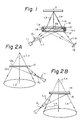
- the optical system comprises a semiconductor laser source 11, a phase hologram 12, a surface relief hologram 13, a (1/4 ⁇ ) wave plate 14, and an optical sensor 15.
- the phase hologram 12 is made of a photosensitive material, such as silver halide, dichromated gelatin, or photopolymer, and is so constructed, as seen from Fig. 2A, that a hologram construction light beam L1 diverging from a point P2 and a converging hologram construction light beam L2 are irradiated onto the above-mentioned photosensitive material.
- a photosensitive material such as silver halide, dichromated gelatin, or photopolymer
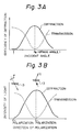
- the phase hologram 12 thus constructed has an incident angle characteristic as shown in Fig. 3A. Apparently, the diffraction efficiency of the phase hologram 12 depends largely on the incident angle of the reconstruction light beam. If a light beam is irradiated to the lower surface 12b of the phase hologram 12 in Fig. 2A, an incident angle of the light beam, which is in the same direction as the hologram construction light beam L1 , is a so called Bragg angle ⁇ B , at which the diffraction efficiency becomes maximum, so that the radiated light beam is diffracted to the direction along an extended line L3 of the hologram construction light beam L2 , as shown by a broken line in Fig. 2A.
- an incident angle of the light beam which is the same direction as the above-mentioned extended line L3 , is the Bragg angle ⁇ B , at which the diffraction efficiency becomes maximum, so that the radiated light beam is diffracted in the direction along the hologram construction light beam L1.
- non-Bragg angle an angle which is at least 20 to 30 degrees away from the above-mentioned Bragg angle
- the surface relief hologram 13 shown in Fig. 1 comprises, as seen from Fig 2B, a (1/4 ⁇ ) wave plate 14 which serves as a substrate, and a coating material, such as photoresist 16, coated on the wave plate 14, onto which a hologram construction light beam L4 diverging from a point P1 and a converging hologram construction light beam L5 are irradiated.
- a plurality of parallel relief grooves directed in one direction are formed on the coated surface.
- the wave plate 14 is used as a substrate, the process for forming holograms is simplified.
- the surface relief hologram 13 thus constructed has a polarization characteristic as shown in Fig. 3B.
- the intensity of a diffracted light beam by this surface relief hologram 13 depends largely upon the direction of polarization of the incident light beam. That is to say, if the direction of the relief grooves is the same as that of the polarization, so-called "S-polarization", the intensity of the diffracted light beam becomes maximum, in which an incident light beam from the same direction as the hologram construction light beam L4 in Fig. 2B is diffracted along an extended line L6 of the hologram construction light beam L5 , as shown by a broken line in Fig. 2B.
- a semiconductor laser source 11 is arranged at a position in which an incident light beam L7 therefrom is irradiated to the phase hologram 12 at the non-Bragg angle.
- the position of laser source 11 corresponds to the focal point P1 of the hologram construction light beam L4 with respect to the surface relief hologram 13.
- the direction A1 of polarization of the above incident light beam L7 from the simiconductor laser 11 is the same as the direction of the relief grooves of the surface relief hologram 13. (The direction A1 is perpendicular to the sheet plane of Fig. 1.)
- the optical sensor 15 is located at a position corresponding to the focal point P2 of the hologram construction light beam L1.
- the hologram 12 and 13 are spaced by a suitable spacer 18 so as to be parallel and adjacent to each other.
- a light beam L7 from the semiconductor laser source 11 is irradiated to the phase hologram 12 at the non-Bragg angle, so that almost all of the incident light beam is transmitted therethrough.
- the transmitted light beam L8 is irradiated to the surface relief hologram 13, but is then diffracted (bent) since the direction (A1) of the polarization is the same as that of the relief grooves.
- the diffracted light beam L9 is focussed via the wave plate 14 on the optical diskette D.
- the diffracted light beam L9 passed through the wave plate 14 has been converted from a linearly polarized light to a circularly polarized light.
- the light beam L10 reflected at the optical diskette D and carrying the read out information is a circularly polarized light, which is the same as the above-mentioned diffracted light beam L9. However, it is converted again to a linearly polarized light when it passes through the wave plate 14, and then is irradiated onto the surface relief hologram 13. However, the direction A2 of the polarization of this incident light beam is parallel to the plane of the sheet of Fig. 1, which is perpendicular to the above direction A1.
- the direction A2 is perpendicular to the direction of the relief grooves of the surface relief hologram 13
- almost all of the incident light beam is transmitted therethrough and the transmitted light beam L11 is irradiated to the phase hologram 12 at the Bragg angle, as mentioned above. Therefore, the transmitted light beam L11 is diffracted and the light beam L12 thus diffracted is introduced into the optical sensor 15.
- Figure 4 shows another embodiment of an optical system according to the present invention, in which the optical system comprises, in the same manner as Fig. 1, a semiconductor laser source 21, a phase hologram 22, a surface relief hologram 23, a (1/4 ⁇ ) wave plate 24, and an optical sensor 25.
- this second embodiment comprises an objective hologram lens 27, which is arranged movably in the direction A3 as well as in the direction perpendicular thereto, so that focussing and tracking the light beam is desirably effected on the optical diskette D by moving the objective hologram lens 27.
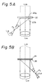
- the phase hologram 22 is made of photosensitive material, in the same manner as the above embodiment, in which a hologram construction light beam L18 (Fig. 5A) diverging from a point P4 and a parallel hologram construction light beam L19 are irradiated onto the photosensitive material.
- the phase hologram 22 thus constructed has a characteristic such that, if a light beam is irradiated onto the lower surface 22b of the phase hologram 22 in Fig. 5A, and if an incident angle of the light beam is in the same direction as the hologram construction light beam L18 (the Bragg angle), the light beam is diffracted as an extended line L20 , as shown by a broken line in Fig. 5A.
- the surface relief hologram 23 is constructed in the same manner as for the above embodiment, in which a photoresist 26 (Fig. 5B) is coated on the wave plate 24, to which a hologram construction light beam L21 diverging from a point P3 and a parallel hologram construction light beam L22 are irradiated. In addition, a plurality of parallel relief grooves directed in one direction are formed on the coated surface.
- the surface relief hologram 23 thus constructed has a polarization characteristic such that if the direction of the relief grooves is the same as that of the polarization, so-called S-polarization, the intensity of the diffracted light beam becomes maximum and an incident light beam from the same direction as the hologram construction light beam L21 in Fig. 5B is diffracted to an extended line L23, as shown by a broken line in Fig. 5B.
- S-polarization the intensity of the diffracted light beam becomes maximum and an incident light beam from the same direction as the hologram construction light beam L21 in Fig. 5B is diffracted to an extended line L23, as shown by a broken line in Fig. 5B.
- P-polarization the intensity of the diffracted light beam becomes minimum and almost all of the incident light beam is transmitted through the surface relief hologram 23.
- the semiconductor laser source 21 is so arranged that the light beam L13 is irradiated therefrom onto the phase hologram 22 at the Bragg angle.
- the direction A4 of polarization of the light beam L13 is parallel to the sheet plane of Fig. 4 and perpendicular to that of the relief grooves of the surface relief hologram 23.
- the light beam L13 from the semiconductor laser source 21 is largely diffracted, since it is irradiated onto the phase hologram 22 at the Bragg angle, as mentioned above.
- the direction A4 of polarization of the light beam L13 is the shorter diametrical direction of an ellipse, as shown in Fig. 6, the shorter diameter is enlarged so that the light beam is compensated into a substantially circular shape by passing through the phase hologram 22.
- the diffracted light beam L14 is then irradiated onto the surface relief hologram 23 and almost all is transmitted therethrough, since the direction of polarization thereof is perpendicular to that of the relief grooves.
- the transmitted light beam is a parallel ray, which is converted to a circularly polarized light when passed through the wave plate 24 and focussed on the optical diskette D by the objective hologram lens 27.
- the light beam L15 reflected at the optical diskette D is again changed to a parallel ray L16 by the objective hologram lens 26 and irradiated onto the surface relief hologram 23 via the wave plate 24.
- the parallel light beam L16 has been converted from a circularly polarized light to a linearly polarized light by the wave plate 24, and the direction A6 of polarization is perpendicular to the sheet plane of Fig. 4, which is the same as the direction of the relief grooves of the surface relief hologram 23.
- the parallel light beam L16 is largely diffracted by the surface relief hologram 23 and the diffracted light beam L17 is irradiated onto the phase hologram 22 at the non-Bragg angle, so that almost all of the light beam is transmitted therethrough and introduced to the optical sensor 25.
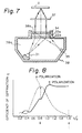
- Figure 7 illustrates a third embodiment of an optical system according to the present invention, in which the optical system comprises, a semiconductor laser source 31, two surface relief holograms 33a and 33b, a (1/4 ⁇ ) wave plate 34, an optical sensor 35, and an objective hologram lens 37.
- the optical system comprises, a semiconductor laser source 31, two surface relief holograms 33a and 33b, a (1/4 ⁇ ) wave plate 34, an optical sensor 35, and an objective hologram lens 37.
- One of the surface relief holograms 33a is constructed on the wave plate 34, in the same manner as in the previous embodiments.
- the light beam from the semiconductor laser source 31 is irradiated onto the surface relief hologram 33b which has a plurality of relief grooves, the direction of which is perpendicular to the polarization of the irradiated light beam. Therefore, the ellipse-shaped light beam is changed to a circular-shaped light beam.
- ⁇ /d (Fig. 8) should be about 0.8, where the central pitch of the relief grooves is d and, of course, the wave length is ⁇ .
- the wave length of the beam from the semiconductor laser source 31 is 0.8 ⁇ m
- d should be about 1 ⁇ m (the spatial frequency is about 1000/mm).
- the light beam diffracted by the surface relief hologram 33b is then irradiated onto the other surface relief hologram 33a which is so constructed that ⁇ /d is about 1.6, i.e., d is about 0.5 ⁇ m (here, the spatial frequency is about 2000/mm) , in order to diffract the light beam only slightly.
- the light beam thus transmitted through the surface relief hologram 33a passes through the wave plate 34 and the objective hologram lens 37 and is focussed on the optical diskette D.
- the reflected light beam is again irradiated onto the surface relief hologram 33a as S-polarization and diffracted thereby. Since the diffracted light beam is S-polarization, it is almost all transmitted through the surface relief hologram 33b and directed toward the optical sensor 35.
- the optical elements including these two holograms 33a and 33b accompanying the wave plate 34, the laser 31, and the optical sensor 35 are accommodated in a single casing structure 38.
- Figure 8 shows the relationship between ⁇ /d and the efficiency of the diffraction ( ⁇ ) in the embodiment shown in Fig. 8.
- ⁇ /d is 0.8
- ⁇ /d is 1.6
- the efficiency of the diffraction of the S-polarization is enlarged.
- Figure 9 illustrates a fourth embodiment similar to the third embodiment shown in Fig. 7.
- the optical system comprises, a semiconductor laser source 41, two surface relief holograms 43a and 43b, a (1/4 ⁇ ) wave plate 44, and an optical sensor 45.
- an objective hologram lens is omitted and, therefore, one of the surface relief holograms 43a is constructed so as to more largely diffract the light beam irradiated from the semiconductor laser source 41 so as to directly focus it on the optical diskette D.
- Figures 10 and 11 illustrate a fifth embodiment similar to the previous embodiment shown in Fig. 9.
- the optical system comprises, a semiconductor laser source 51, two surface relief holograms 53a and 53b, a (1/4 ⁇ ) wave plate 54, and an optical sensor 55, in the same manner as in the previous embodiment shown in Fig. 9.
- the two surface relief holograms 53a and 53b are arranged in such a manner that the relief grooves of one of the holograms extend perpendicular with respect to those of the other hologram.
- the laser source 51 and the optical sensor 55 can be arranged on x and y lines, respectively, if the laser beam is irradiated along z line toward the optical diskette D, in the x,y,z-coordinates.
- Reference numeral 52 in Fig. 11 denotes a flat mirror, arranged in parallel to the y,z-plane in Fig. 10, for reflecting the light beam irradiated from the laser source 51.
- the laser source 51 can be located in the vicinity of the 0-point, i.e., the intersection of the lines x, y, and z.
- the optical pickup can be constructed in a more compact size.
- Figures 12 and 13 illustrate a sixth embodiment of an optical system according to the present invention, in which the optical system comprises a semiconductor laser source 61, two phase holograms 62a and 62b, a (1/4 ⁇ ) wave plate 64, and an optical sensor 65.
- the light beam from the semiconductor laser source 61 is irradiated onto the phase hologram 62b at the non-Bragg angle, so that almost all of the incident light beam is transmitted therethrough.
- the direction of polarization is A1 , which is perpendicular to the sheet plane of Fig. 12.
- the light beam is then irradiated onto the other phase hologram 62a.
- a phase hologram can also have the same characteristics as FIG. 3B.
- the light beam reflected at the optical diskette D passes through the wave plate 64, it is again converted to a linearly polarized light, the direction of which is A2 , perpendicular to the above direction A1 , and then irradiated onto the phase hologram 62a, bacause of S-polarization, almost all of the incident light beam is transmitted therethrough.
- the light beam is then irradiated onto the phase hologram 62b at the Bragg angle. Therefore, the light beam is diffracted thereby and directed to the optical sensor 65.
- the two phase holograms 62a and 62b and the wave plate 64 may be laminated as shown in Fig. 13 and constructed as a compact optical module together with the laser source 61 and the optical sensor 65.
- Embodiments of the laminated phase holograms 62a and 62b and wave plate 64 are illustrated in Figs. 14 and 15.
- a) hologram material 62b', such as PVCz, is coated on a transparent substrate 66 to obtain the phase hologram 62b; b) on which a Si protection film 67b is formed to protect it from the subsequent chemical processes for making the other phase hologram 62a.
- Hologram material 62a' such as PVCz
- Si protection film 67a is formed on the phase hologram 62a to protect it and the (1/4 ⁇ ) wave plate 64 is adhered to the phase hologram 62a via optical adhesion (adhesive) 68.
- reflection protecting films 69 can be coated to reduce the possible optical loss. The thickness of such laminated holograms does not greatly exceed the sum of thickness of the substrate 66 and the wave plate 64.
- hologram material 62b' is coated on a transparent substrate 66 and hologram material 62a' is directly coated on the (1/4 ⁇ ) wave plate 64, respectively. b) Then these two hologram layers are adhered in a face-to-face relationship via an optical adhesive 68. If necessary for the kinds of hologram material, to protect the hologram layers with respect to the adhesive, protection films can be formed on these hologram layers before adhesion.
- a hologram lens which can be used as the objective hologram lens 27 (Fig. 4) or 37 (Fig. 7).
- H1 denotes a first hologram lens; and H2, a second hologram lens.
- the first hologram lens H1 is located to face an incident light 71.
- the second hologram lens H2 is located at the side of a focal point 74.
- the first and second hologram lens H1 and H2 are shown to be separated for only the convenience of explanation, they preferably constitute a laminated structure in the same manner as described with reference to Figs. 14 and 15.
- the first hologram lens H1 serves to diffract the incident light beam 71 to the diverging direction with respect to an optical axis A.
- the second hologram lens H2 serves to diffract the light beam 72 diffracted by the first hologram H1 to the converging direction with respect to the optical axis A.
- the incident light 71 is diffracted outward when it passes through the first hologram lens H1. Then, diffracted light beam 72 is again diffracted inward when it passes through the second hologram lens H2.
- the converging light beam 73 is focussed on the focal point 74.
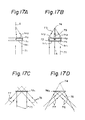
- Figures 17A, 17B, 17C and 17D illustrate a first embodiment of the objective hologram lens, wherein Fig. 17A shows a right half of the double-structured hologram lens as described above. Two sets of the right halves of double-structured hologram lens are to be prepared, and one of them is turned over 180°C about the optical axis A and abutted to the other half of hologram lens, as shown in Fig. 17B.
- the first hologram lens H1 generates plane wave diverging to the periphery, when a symmetrical light beam with respect to the optical axis A, such as plane wave perpendicular to the hologram, is introduced to the first hologram H1.
- the second hologram lens H2 serves to diffract the light beam 72 diffracted by the first hologram H1 to focus it on the focal point 74.
- These first and second hologram lens H1 and H2 are adhered to each other by a suitable optical adhesion, such as a type wherein the adhesive is hardened by ultraviolet radiation.
- Two right halves of the double-structured hologram lens thus made are aligned side by side on a line to make an inline hologram lens having a good property in a reasonable range of spatial frequency.
- a spherical wave 78 is irradiated onto the whole plane of the second hologram H2 , and plane waves 76 and 77 are irradiated obliquely onto the right half and the left half, respectively, to produce interference fringes.
- the first hologram H1 is made by irradiating two separated plane waves 76 and 77 from the respective directions so as to superimpose these plane waves 76 and 77 around the center of one hologram material H P1 , thereby two holograms can be precisely and smoothly joined.
- the second hologram H2 is also made by irradiating these left and right plane waves 76 and 77 so as to superimpose parts of them onto the optical axis A. To prevent a mutual interference by the plane waves 76 and 77 themselves, it is advantageous to use suitable masks and to conduct the optical deposition in two steps.
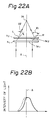
- the range of spatial frequency can be narrowed to about a half of that of a conventional hologram lens, as shown by B in Fig. 23, and thus an improvement of the optical efficiency over the whole area of the hologram can be expected.
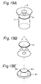
- Figures 19A, 19B, 19C, 19D, and 19E show a third embodiment of the objective hologram lens, in which the optical path is symmetrical with respect to the optical axis A.
- the first hologram H1 is constructed so that the interference fringes thereof are such that, if an incident light wave (such as a plane wave perpendicularly irradiated) which is symmetrical to the optical axis A is applied to the hologram, the light wave is irradiated from circles onto the hologram concentric about the optical axis A and along the slant lines of the concentric circular cones, as seen from Fig. 19A.
- an incident light wave such as a plane wave perpendicularly irradiated
- the second hologram H2 is constructed so that the interference fringes thereof are such that, if an incident light wave is applied thereto along slant lines of circular cones concentric about the optical axis A, the light wave is irradiated therefrom to focus on a point on the optical axis A, as seen from Fig. 19B.
- These two holograms H1 and H2 are laminated to make a double-structured (inline) hologram lens.
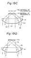
- Figures 19C and 19D show processes for making these two holograms H1 and H2 , respectively, in which reference numeral 81 denotes a transparent optical element having a cone slant face 82, as also shown in Fig. 19E. to construct the first hologram H1.
- a ring-shaped plane wave 83 is irradiated onto the cone face 82 of the optical element 81 and circular plane wave 84 is also irradiated onto the central plane surface 84.
- the plane wave 83 is diffracted at the respective faces of the optical element 81, so that the inner periphery thereof is focussed on the optical axis A and the outer periphery thereof is focussed on the outer periphery of the hologram material Hp1 to construct interference fringes functioning as explained with reference to Fig. 19A.
- the hologram material Hp2 is placed at a retracted position, as shown by a dotted line in Fig. 19C and a solid line in Fig. 19D.
- a spherical wave 78 is also irradiated onto the plane surface 84, thereby interference fringes functioning as explained with reference to Fig. 19B are formed.
- the optical element 81 may have a central opening 86 (Figs. 19C and 19E) for passing through the spherical wave 78.
- Figure 20 shows a fourth embodiment of a hologram lens, in which the optical element 81 is placed so that the cone slant face 82 thereof faces to the hologram materials.
- the hologram materials for the first and second holograms H1 and H2 are placed at Hp1 and Hp2 , respectively, to construct these holograms H1 and H2.
- the hologram lens thus made in accordance with the third and fourth embodiments, it is also possible to set a narrow range of spatial frequency, as for B in Fig. 23, and an improvement of the optical efficiency over the whole area of the hologram can be expected.
- an inline hologram lens as constructed in accordance with the present invention has an advantageously narrow range of spatial frequency.
- the spatial frequency of the interference fringes at the right end R is different from that at the left end L, and the spatial frequency continuously changes.
- the hologram lens has an advantageously narrow range of spatial frequency, as seen at B in Fig. 23.
Landscapes
- Physics & Mathematics (AREA)
- Optics & Photonics (AREA)
- General Physics & Mathematics (AREA)
- Diffracting Gratings Or Hologram Optical Elements (AREA)
- Optical Head (AREA)
- Holo Graphy (AREA)
Claims (11)
- Capteur optique comprenant une source de lumière (11, 21, 31, 41, 51, 61) pour irradier un faisceau de lumière sur un support d'enregistrement d'information (D) tel qu'une disquette optique, un détecteur optique (15, 25, 35, 45, 55, 65) pour détecter le faisceau de lumière réfléchi par ledit support d'enregistrement d'information et un système de lentille optique incluant :
une lame d'onde (14, 24, 34, 44, 54, 64), une première lentille d'hologramme (12, 22, 33b, 43b, 53b, 62b) et une seconde lentille d'hologramme (13, 23, 33a, 43a, 53a, 62a) agencées sensiblement parallèlement l'une à l'autre ; le système de lentille optique étant agencé pour diriger le faisceau lumineux irradié depuis ladite source de lumière le long d'un premier chemin en direction dudit support et pour diriger le faisceau lumineux réfléchi par ledit support d'enregistrement d'information le long d'un second chemin en direction dudit détecteur ; dans lequel
l'une (13, 22, 33b, 43b, 53a, 62a) desdites lentilles d'hologramme fonctionne pour diffracter le faisceau lumineux qui provient de la source de lumière en direction dudit support d'enregistrement d'information (D) et l'autre lentille d'hologramme (12, 23, 33a, 43a, 53b, 62b) fonctionne pour transmettre le faisceau lumineux qui provient de ladite source de lumière et pour diffracter le faisceau lumineux réfléchi qui provient dudit support d'enregistrement d'information en direction du détecteur optique ; caractérisé en ce que :
lesdites lentilles d'hologramme et la lame d'onde sont agencées de telle sorte que le faisceau lumineux reçu directement depuis ladite source de lumière suive ledit premier chemin en traversant lesdites première et seconde lentilles d'hologramme et ladite lame d'onde à la suite et le faisceau lumineux réfléchi suive ledit second chemin en traversant ladite lame d'onde et lesdites seconde et première lentilles d'hologramme à la suite pour être directement reçu par ledit détecteur optique ; et en ce que
ladite une des lentilles d'hologramme fonctionne également pour transmettre le faisceau lumineux réfléchi qui provient dudit support d'enregistrement (D) de telle sorte que chaque chemin comprenne une fonction de lentille d'hologramme de diffraction et de transmission. - Capteur optique selon la revendication 1, dans lequel ladite une (13, 43b, 53a, 62a) desdites lentilles d'hologramme diffracte le faisceau lumineux qui provient de ladite source de lumière (11, 41, 51, 61) de manière à le focaliser directement sur ledit support d'enregistrement d'information (D).
- Capteur optique selon la revendication 1 ou 2, dans lequel ladite autre (12, 23, 33a, 43a, 53b, 62b) desdites lentilles d'hologramme diffracte le faisceau lumineux réfléchi qui provient dudit support d'enregistrement d'information (D) de manière à le focaliser sur ledit détecteur optique (15, 25, 35, 45, 55, 65).
- Capteur optique selon la revendication 1, 2 ou 3, dans lequel ladite source lumineuse (11, 21, 31, 41, 51, 61) est un laser à semiconducteur.
- Capteur optique selon l'une quelconque des revendications précédentes, dans lequel lesdites première et seconde lentilles d'hologramme sont constituées par un hologramme de phase (12, 22) qui, lors de son utilisation, transmet le faisceau lumineux en l'irradiant selon l'angle de non Bragg et diffracte le faisceau lumineux en l'irradiant selon l'angle de Bragg, et l'autre lentille d'hologramme est constituée par un hologramme de relief de surface (13, 23).
- Capteur optique selon la revendication 1, 2, 3 ou 4, dans lequel lesdites première et seconde lentilles d'hologramme sont toutes deux constituées par des hologrammes de phase (62a, 62b), la lentille d'hologramme (62a) qui est adjacente au support d'enregistrement d'information (D) transmet ou diffracte, lorsqu'elle est utilisée, le faisceau lumineux en l'irradiant selon l'angle de non Bragg ou selon l'angle de Bragg, et l'autre lentille d'hologramme (62b), lorsqu'elle est utilisée, transmet ou diffracte le faisceau lumineux en l'irradiant selon l'angle de non Bragg ou selon l'angle de Bragg ou selon une polarisation P ou S.
- Capteur optique selon la revendication 1, 2, 3 ou 4, dans lequel lesdites première et seconde lentilles d'hologrammes sont toutes deux constituées par des hologrammes de relief de surface (33a, 33b ; 53a, 53b).
- Capteur optique selon la revendication 7, dans lequel lesdites première et seconde lentilles d'hologramme de relief de surface (33a, 33b) ont des gorges de relief et les gorges de relief de la première lentille d'hologramme sont agencées parallèlement à celles de la seconde lentille d'hologramme.
- Capteur optique selon la revendication 7, dans lequel lesdites première et seconde lentilles d'hologramme de relief de surface (53a, 53b) ont des gorges de relief et les gorges de relief de le première lentille d'hologramme sont agencées perpendiculairement à celles de la seconde lentille d'hologramme.
- Capteur optique selon l'une quelconque des revendications précédentes, dans lequel l'une (22, 33b) desdites première et seconde lentilles d'hologramme, lorsqu'elle est utilisée, diffracte le faisceau lumineux qui provient de ladite source de lumière (21, 31) afin de former un faisceau lumineux parallèle et ledit système de lentille optique comprend en outre une lentille d'objectif à hologramme (27, 37) pour focaliser ledit faisceau lumineux parallèle sur ledit support d'enregistrement d'information (D).
- Capteur optique selon la revendication 10, dans lequel ladite lentille d'objectif à hologramme (27, 37) est une lentille d'hologramme en ligne à double structure qui est symétrique par rapport à son axe optique (A).
Applications Claiming Priority (6)
| Application Number | Priority Date | Filing Date | Title |
|---|---|---|---|
| JP57456/85 | 1985-03-20 | ||
| JP60057456A JPS61246940A (ja) | 1985-03-20 | 1985-03-20 | 光ピツクアツプ |
| JP260317/85 | 1985-11-20 | ||
| JP60260317A JPS62120640A (ja) | 1985-11-20 | 1985-11-20 | 光ピツクアツプ |
| JP61003337A JP2526206B2 (ja) | 1986-01-10 | 1986-01-10 | 光ピツクアツプ |
| JP3337/86 | 1986-01-10 |
Publications (3)
| Publication Number | Publication Date |
|---|---|
| EP0195657A2 EP0195657A2 (fr) | 1986-09-24 |
| EP0195657A3 EP0195657A3 (en) | 1988-12-07 |
| EP0195657B1 true EP0195657B1 (fr) | 1992-07-01 |
Family
ID=27275774
Family Applications (1)
| Application Number | Title | Priority Date | Filing Date |
|---|---|---|---|
| EP86301994A Expired - Lifetime EP0195657B1 (fr) | 1985-03-20 | 1986-03-19 | Capteur optique |
Country Status (5)
| Country | Link |
|---|---|
| US (1) | US4824191A (fr) |
| EP (1) | EP0195657B1 (fr) |
| KR (1) | KR900002999B1 (fr) |
| CA (1) | CA1257392A (fr) |
| DE (1) | DE3685831T2 (fr) |
Families Citing this family (30)
| Publication number | Priority date | Publication date | Assignee | Title |
|---|---|---|---|---|
| FR2597249B1 (fr) * | 1986-04-11 | 1988-06-17 | Thomson Csf | Dispositif de lecture optique de support d'enregistrement optique |
| KR910002322B1 (ko) * | 1986-09-20 | 1991-04-11 | 후지쓰 가부시끼가이샤 | 회절격자렌즈 조립체를 구비하고 있는 광학시스템 |
| US4969700A (en) * | 1987-12-23 | 1990-11-13 | American Bank Note Holographics, Inc. | Computer aided holography and holographic computer graphics |
| US4789977A (en) * | 1986-11-06 | 1988-12-06 | Laser Magnetic Storage International Company | Optical data recording device |
| JPH0738260B2 (ja) * | 1987-04-01 | 1995-04-26 | 日本電気株式会社 | 光磁気用光ヘツド装置 |
| DE3855936T2 (de) * | 1987-08-24 | 1998-01-02 | Sharp Kk | Optische Abtastvorrichtung |
| FR2621411B1 (fr) | 1987-10-05 | 1989-12-08 | Bull Sa | Dispositif asservi de lecture optique et d'ecriture magnetique d'un support d'informations |
| US5115423A (en) * | 1988-01-07 | 1992-05-19 | Ricoh Company, Ltd. | Optomagnetic recording/reproducing apparatus |
| US4924507A (en) * | 1988-02-11 | 1990-05-08 | The United States Of America As Represented By The Administrator Of The National Aeronautics And Space Administration | Real-time optical multiple object recognition and tracking system and method |
| JPH01311428A (ja) * | 1988-06-09 | 1989-12-15 | Matsushita Electric Ind Co Ltd | 光ヘッド装置及びこれを用いた光情報装置 |
| DE68924303T2 (de) * | 1988-06-14 | 1996-02-29 | Nippon Electric Co | Optische Kopfanordnung. |
| EP0348221B1 (fr) * | 1988-06-23 | 1994-12-14 | Sharp Kabushiki Kaisha | Appareil de reproduction optique |
| US4983017A (en) * | 1988-08-02 | 1991-01-08 | Sharp Kabushiki Kaisha | Optical head device for reading information stored in a recording medium |
| US5013107A (en) * | 1988-09-15 | 1991-05-07 | Biles Jonathan R | Polarization selective holographic optical element |
| US4993789A (en) * | 1988-09-15 | 1991-02-19 | Jonathan R. Biles | Dual wavelength polarization selective holographic optical element |
| FR2639460B1 (fr) * | 1988-11-21 | 1993-05-21 | Ricoh Kk | Appareil d'enregistrement/reproduction optique |
| NL8802988A (nl) * | 1988-12-05 | 1990-07-02 | Philips Nv | Inrichting voor het met optische straling aftasten van een informatievlak. |
| US5237451A (en) * | 1989-11-17 | 1993-08-17 | Minnesota Mining And Manufacturing Company | Beam shaping system using diffraction |
| JP2663734B2 (ja) * | 1991-03-13 | 1997-10-15 | 松下電器産業株式会社 | 露光装置 |
| JPH0589546A (ja) * | 1991-09-27 | 1993-04-09 | Sharp Corp | 光磁気記録再生装置における光ピツクアツプ装置 |
| US5272550A (en) * | 1991-10-11 | 1993-12-21 | International Business Machines Corporation | Hologram system |
| US5410468A (en) * | 1992-06-26 | 1995-04-25 | Matsushita Electric Industrial Co., Ltd. | Optical pick-up apparatus |
| DE69318770T2 (de) * | 1992-07-30 | 1998-10-15 | Matsushita Electric Ind Co Ltd | Optisches Wiedergabegerät |
| KR950005033B1 (ko) * | 1992-11-06 | 1995-05-17 | 주식회사금성사 | 광픽업 장치 |
| US5491569A (en) * | 1994-06-17 | 1996-02-13 | Northeast Photosciences | High efficiency, broad bandwidth, volume holographic element for diffraction windows and method of manufacture |
| US5517339A (en) * | 1994-06-17 | 1996-05-14 | Northeast Photosciences | Method of manufacturing high efficiency, broad bandwidth, volume holographic elements and solar concentrators for use therewith |
| US5758955A (en) * | 1995-07-11 | 1998-06-02 | High End Systems, Inc. | Lighting system with variable shaped beam |
| JP2001326290A (ja) * | 2000-03-10 | 2001-11-22 | Seiko Epson Corp | パッケージの封止方法、電子素子モジュールの製造方法、封止装置並びにパッケージ品 |
| US7647277B1 (en) | 2002-10-25 | 2010-01-12 | Time Warner Inc. | Regulating access to content using a multitiered rule base |
| US7315946B1 (en) * | 2003-04-14 | 2008-01-01 | Aol Llc | Out-of-band tokens for rights access |
Family Cites Families (7)
| Publication number | Priority date | Publication date | Assignee | Title |
|---|---|---|---|---|
| DE2123833A1 (de) * | 1971-05-13 | 1972-11-23 | Siemens AG, 1000 Berlin u. 8000 München | Kohärent optischer Vielkanalkorrelator |
| DE2315776A1 (de) * | 1973-03-29 | 1974-10-10 | Siemens Ag | Holografiespeicher |
| AU535350B2 (en) * | 1979-05-07 | 1984-03-15 | Sony Corporation | Inline hologram lens |
| JPS5647933A (en) * | 1979-09-25 | 1981-04-30 | Sony Corp | Optical signal head |
| JPS56161582A (en) * | 1980-05-14 | 1981-12-11 | Sony Corp | Production of in-line hologram lens |
| US4488042A (en) * | 1982-04-15 | 1984-12-11 | Honeywell Inc. | Line scan reader/writer by holographic collection |
| US4497534A (en) * | 1983-02-28 | 1985-02-05 | International Business Machines Corporation | Holographic optical head |
-
1986
- 1986-03-12 CA CA000503923A patent/CA1257392A/fr not_active Expired
- 1986-03-19 EP EP86301994A patent/EP0195657B1/fr not_active Expired - Lifetime
- 1986-03-19 DE DE8686301994T patent/DE3685831T2/de not_active Expired - Fee Related
- 1986-03-20 KR KR8602065A patent/KR900002999B1/ko not_active Expired
-
1988
- 1988-03-28 US US07/173,050 patent/US4824191A/en not_active Expired - Lifetime
Also Published As
| Publication number | Publication date |
|---|---|
| EP0195657A3 (en) | 1988-12-07 |
| DE3685831D1 (de) | 1992-08-06 |
| KR900002999B1 (en) | 1990-05-04 |
| KR860007644A (ko) | 1986-10-15 |
| CA1257392A (fr) | 1989-07-11 |
| EP0195657A2 (fr) | 1986-09-24 |
| US4824191A (en) | 1989-04-25 |
| DE3685831T2 (de) | 1993-02-04 |
Similar Documents
| Publication | Publication Date | Title |
|---|---|---|
| EP0195657B1 (fr) | Capteur optique | |
| EP0803867B1 (fr) | Dispositif de tête optique | |
| US5272550A (en) | Hologram system | |
| US5331445A (en) | Increased Bragg angle sensitivity hologram system and method | |
| US4789977A (en) | Optical data recording device | |
| KR970003373B1 (ko) | 홀로그램 시스템 및 방법 | |
| US5515354A (en) | Optical pickup | |
| EP0545735B1 (fr) | Appareil de lecture optique | |
| EP0803867A1 (fr) | Dispositif de tête optique | |
| EP0780838B1 (fr) | Appareil de lecture optique, objectif et système optique convergent pour appareil de lecture optique et appareil de disque optique | |
| US4993789A (en) | Dual wavelength polarization selective holographic optical element | |
| US5272690A (en) | Hologram element system | |
| US7313072B2 (en) | Method for recording and reproducing holographic data and holographic recording medium | |
| US5051974A (en) | Optical head device having a light splitter with a diffraction grating structure | |
| US20040156083A1 (en) | Holographic recording/reproducing apparatus and reproducing apparatus for holographically recorded information | |
| EP0545524A1 (fr) | Système d'hologramme | |
| KR100368493B1 (ko) | 홀로그램 패턴을 이용한 광픽업 장치 및 홀로그램 패턴발생 방법 | |
| US5311495A (en) | Optical system for converging light beams to form a single beam spot on an optical disc | |
| US5946137A (en) | Optical information processing unit | |
| JP3658928B2 (ja) | 光ヘッド装置 | |
| JPH0797162B2 (ja) | 光ビ−ム拡大器 | |
| JPS61246940A (ja) | 光ピツクアツプ | |
| JPH1131332A5 (fr) | ||
| JP2526206B2 (ja) | 光ピツクアツプ | |
| JPS633381B2 (fr) |
Legal Events
| Date | Code | Title | Description |
|---|---|---|---|
| PUAI | Public reference made under article 153(3) epc to a published international application that has entered the european phase |
Free format text: ORIGINAL CODE: 0009012 |
|
| AK | Designated contracting states |
Kind code of ref document: A2 Designated state(s): BE DE FR GB IT NL |
|
| PUAL | Search report despatched |
Free format text: ORIGINAL CODE: 0009013 |
|
| AK | Designated contracting states |
Kind code of ref document: A3 Designated state(s): BE DE FR GB IT NL |
|
| 17P | Request for examination filed |
Effective date: 19890215 |
|
| 17Q | First examination report despatched |
Effective date: 19900528 |
|
| ITF | It: translation for a ep patent filed | ||
| GRAA | (expected) grant |
Free format text: ORIGINAL CODE: 0009210 |
|
| AK | Designated contracting states |
Kind code of ref document: B1 Designated state(s): BE DE FR GB IT NL |
|
| REF | Corresponds to: |
Ref document number: 3685831 Country of ref document: DE Date of ref document: 19920806 |
|
| ET | Fr: translation filed | ||
| ITTA | It: last paid annual fee | ||
| PLBE | No opposition filed within time limit |
Free format text: ORIGINAL CODE: 0009261 |
|
| STAA | Information on the status of an ep patent application or granted ep patent |
Free format text: STATUS: NO OPPOSITION FILED WITHIN TIME LIMIT |
|
| 26N | No opposition filed | ||
| PGFP | Annual fee paid to national office [announced via postgrant information from national office to epo] |
Ref country code: DE Payment date: 20010312 Year of fee payment: 16 |
|
| PGFP | Annual fee paid to national office [announced via postgrant information from national office to epo] |
Ref country code: FR Payment date: 20010313 Year of fee payment: 16 |
|
| PGFP | Annual fee paid to national office [announced via postgrant information from national office to epo] |
Ref country code: GB Payment date: 20010314 Year of fee payment: 16 |
|
| PGFP | Annual fee paid to national office [announced via postgrant information from national office to epo] |
Ref country code: NL Payment date: 20010330 Year of fee payment: 16 |
|
| PGFP | Annual fee paid to national office [announced via postgrant information from national office to epo] |
Ref country code: BE Payment date: 20010516 Year of fee payment: 16 |
|
| REG | Reference to a national code |
Ref country code: GB Ref legal event code: IF02 |
|
| PG25 | Lapsed in a contracting state [announced via postgrant information from national office to epo] |
Ref country code: GB Free format text: LAPSE BECAUSE OF NON-PAYMENT OF DUE FEES Effective date: 20020319 |
|
| PG25 | Lapsed in a contracting state [announced via postgrant information from national office to epo] |
Ref country code: BE Free format text: LAPSE BECAUSE OF NON-PAYMENT OF DUE FEES Effective date: 20020331 |
|
| BERE | Be: lapsed |
Owner name: *FUJITSU LTD Effective date: 20020331 |
|
| PG25 | Lapsed in a contracting state [announced via postgrant information from national office to epo] |
Ref country code: NL Free format text: LAPSE BECAUSE OF NON-PAYMENT OF DUE FEES Effective date: 20021001 Ref country code: DE Free format text: LAPSE BECAUSE OF NON-PAYMENT OF DUE FEES Effective date: 20021001 |
|
| GBPC | Gb: european patent ceased through non-payment of renewal fee |
Effective date: 20020319 |
|
| PG25 | Lapsed in a contracting state [announced via postgrant information from national office to epo] |
Ref country code: FR Free format text: LAPSE BECAUSE OF NON-PAYMENT OF DUE FEES Effective date: 20021129 |
|
| NLV4 | Nl: lapsed or anulled due to non-payment of the annual fee |
Effective date: 20021001 |
|
| REG | Reference to a national code |
Ref country code: FR Ref legal event code: ST |
|
| PG25 | Lapsed in a contracting state [announced via postgrant information from national office to epo] |
Ref country code: IT Free format text: LAPSE BECAUSE OF NON-PAYMENT OF DUE FEES;WARNING: LAPSES OF ITALIAN PATENTS WITH EFFECTIVE DATE BEFORE 2007 MAY HAVE OCCURRED AT ANY TIME BEFORE 2007. THE CORRECT EFFECTIVE DATE MAY BE DIFFERENT FROM THE ONE RECORDED. Effective date: 20050319 |