EP0195935A2 - Procédé de fabrication d'un substrat comportant des parties rigides et flexibles pour circuits imprimés - Google Patents
Procédé de fabrication d'un substrat comportant des parties rigides et flexibles pour circuits imprimés Download PDFInfo
- Publication number
- EP0195935A2 EP0195935A2 EP86102244A EP86102244A EP0195935A2 EP 0195935 A2 EP0195935 A2 EP 0195935A2 EP 86102244 A EP86102244 A EP 86102244A EP 86102244 A EP86102244 A EP 86102244A EP 0195935 A2 EP0195935 A2 EP 0195935A2
- Authority
- EP
- European Patent Office
- Prior art keywords
- rigid
- circuit board
- insulating material
- flexible
- plate
- Prior art date
- Legal status (The legal status is an assumption and is not a legal conclusion. Google has not performed a legal analysis and makes no representation as to the accuracy of the status listed.)
- Withdrawn
Links
- 238000000034 method Methods 0.000 title claims description 28
- 238000004519 manufacturing process Methods 0.000 title claims description 17
- 239000011810 insulating material Substances 0.000 claims abstract description 62
- 239000004020 conductor Substances 0.000 claims abstract description 55
- RYGMFSIKBFXOCR-UHFFFAOYSA-N Copper Chemical compound [Cu] RYGMFSIKBFXOCR-UHFFFAOYSA-N 0.000 claims abstract description 22
- 230000007704 transition Effects 0.000 claims abstract description 13
- 239000011889 copper foil Substances 0.000 claims abstract description 11
- 239000011888 foil Substances 0.000 claims description 17
- 230000001681 protective effect Effects 0.000 claims 8
- 239000012774 insulation material Substances 0.000 claims 1
- 239000002313 adhesive film Substances 0.000 abstract description 20
- 229910052802 copper Inorganic materials 0.000 abstract description 10
- 239000010949 copper Substances 0.000 abstract description 10
- 230000015572 biosynthetic process Effects 0.000 abstract description 2
- 239000010410 layer Substances 0.000 description 47
- 239000010408 film Substances 0.000 description 31
- 239000000126 substance Substances 0.000 description 9
- 239000000853 adhesive Substances 0.000 description 8
- 230000001070 adhesive effect Effects 0.000 description 8
- 206010041953 Staring Diseases 0.000 description 6
- 239000013039 cover film Substances 0.000 description 5
- 238000007747 plating Methods 0.000 description 5
- 229920001721 polyimide Polymers 0.000 description 5
- 239000012790 adhesive layer Substances 0.000 description 4
- 239000003822 epoxy resin Substances 0.000 description 4
- 229920000647 polyepoxide Polymers 0.000 description 4
- 239000004642 Polyimide Substances 0.000 description 3
- 238000005520 cutting process Methods 0.000 description 3
- 239000003792 electrolyte Substances 0.000 description 3
- 230000035515 penetration Effects 0.000 description 3
- 150000001879 copper Chemical class 0.000 description 2
- 238000005530 etching Methods 0.000 description 2
- 239000003365 glass fiber Substances 0.000 description 2
- 240000005702 Galium aparine Species 0.000 description 1
- 238000005253 cladding Methods 0.000 description 1
- 230000001419 dependent effect Effects 0.000 description 1
- 238000011161 development Methods 0.000 description 1
- 230000018109 developmental process Effects 0.000 description 1
- 230000000694 effects Effects 0.000 description 1
- 239000004744 fabric Substances 0.000 description 1
- 238000009413 insulation Methods 0.000 description 1
- 239000004922 lacquer Substances 0.000 description 1
- 239000002648 laminated material Substances 0.000 description 1
- 239000000463 material Substances 0.000 description 1
- 238000003801 milling Methods 0.000 description 1
- 230000002093 peripheral effect Effects 0.000 description 1
- 229920005989 resin Polymers 0.000 description 1
- 239000011347 resin Substances 0.000 description 1
Images

Classifications
-
- H—ELECTRICITY
- H05—ELECTRIC TECHNIQUES NOT OTHERWISE PROVIDED FOR
- H05K—PRINTED CIRCUITS; CASINGS OR CONSTRUCTIONAL DETAILS OF ELECTRIC APPARATUS; MANUFACTURE OF ASSEMBLAGES OF ELECTRICAL COMPONENTS
- H05K1/00—Printed circuits
- H05K1/02—Details
- H05K1/0213—Electrical arrangements not otherwise provided for
- H05K1/0216—Reduction of cross-talk, noise or electromagnetic interference
-
- H—ELECTRICITY
- H05—ELECTRIC TECHNIQUES NOT OTHERWISE PROVIDED FOR
- H05K—PRINTED CIRCUITS; CASINGS OR CONSTRUCTIONAL DETAILS OF ELECTRIC APPARATUS; MANUFACTURE OF ASSEMBLAGES OF ELECTRICAL COMPONENTS
- H05K3/00—Apparatus or processes for manufacturing printed circuits
- H05K3/46—Manufacturing multilayer circuits
- H05K3/4688—Composite multilayer circuits, i.e. comprising insulating layers having different properties
- H05K3/4691—Rigid-flexible multilayer circuits comprising rigid and flexible layers, e.g. having in the bending regions only flexible layers
-
- H—ELECTRICITY
- H05—ELECTRIC TECHNIQUES NOT OTHERWISE PROVIDED FOR
- H05K—PRINTED CIRCUITS; CASINGS OR CONSTRUCTIONAL DETAILS OF ELECTRIC APPARATUS; MANUFACTURE OF ASSEMBLAGES OF ELECTRICAL COMPONENTS
- H05K1/00—Printed circuits
- H05K1/02—Details
- H05K1/03—Use of materials for the substrate
- H05K1/0313—Organic insulating material
- H05K1/0353—Organic insulating material consisting of two or more materials, e.g. two or more polymers, polymer + filler, + reinforcement
- H05K1/036—Multilayers with layers of different types
-
- H—ELECTRICITY
- H05—ELECTRIC TECHNIQUES NOT OTHERWISE PROVIDED FOR
- H05K—PRINTED CIRCUITS; CASINGS OR CONSTRUCTIONAL DETAILS OF ELECTRIC APPARATUS; MANUFACTURE OF ASSEMBLAGES OF ELECTRICAL COMPONENTS
- H05K2201/00—Indexing scheme relating to printed circuits covered by H05K1/00
- H05K2201/03—Conductive materials
- H05K2201/0332—Structure of the conductor
- H05K2201/0335—Layered conductors or foils
- H05K2201/0355—Metal foils
-
- H—ELECTRICITY
- H05—ELECTRIC TECHNIQUES NOT OTHERWISE PROVIDED FOR
- H05K—PRINTED CIRCUITS; CASINGS OR CONSTRUCTIONAL DETAILS OF ELECTRIC APPARATUS; MANUFACTURE OF ASSEMBLAGES OF ELECTRICAL COMPONENTS
- H05K2201/00—Indexing scheme relating to printed circuits covered by H05K1/00
- H05K2201/09—Shape and layout
- H05K2201/09009—Substrate related
- H05K2201/0909—Preformed cutting or breaking line
Definitions
- the present invention relates to a method for producing a rigid and flexible circuit board for printed electrical circuits, in which at least one rigid and at least one flexible insulating material layer are sandwiched together, the rigid insulating material layer only covers parts of the flexible insulating material layer and at least the flexible insulating material layer electrically Carries conductor tracks.
- Printed circuit boards of the type mentioned as well as various methods for producing the same are known.
- Several of the known production methods each start from a plate which forms the future rigid insulating material layer and which has larger dimensions than the printed circuit board to be produced.
- This plate will be provided with continuous slots at the future transition points between a rigid and a flexible part of the circuit board, the ends of which lie within the contours of the plate, but outside the future contours of the circuit board to be produced.
- a flexible film forming the future flexible insulating material layer is arranged on one side of the board, running over the slots thereof, and connected to the board by means of an adhesive film placed therebetween using pressure and heat.
- the flexible film carries electrical conductor tracks or on its side facing away from the plate a copper layer from which electrical conductor tracks can be formed.
- the conductor tracks and associated bores in the printed circuit board are then finished in the customary manner, after which the plate and the flexible film connected to it are severed along the contour lines of the printed circuit board, the contour lines crossing the end parts of the slots in the plate.
- the area bounded by the slots and the K o ntur baine and future Parts of the board covering flexible parts of the printed circuit board are finally detached from the flexible film and removed.
- a rigid board is generally used, which is laminated on its side to be turned away from the flexible film with a copper layer, which allows the formation of conductor tracks.
- a flexible insulating material film is used, which is laminated on its side to be turned away from the rigid plate with a copper layer to form conductor tracks.
- the desired conductor tracks can be produced in a known manner from the aforementioned copper layers in a photo-chemical way, and conductor holes on one and on the other side of the circuit board can be electrically connected to one another by means of associated bores and galvanic plating.
- the slits created in the rigid plate may have a disruptive effect because these slits are open on the side of the rigid plate facing away from the flexible film and allow the entry of chemicals and other foreign substances. This is particularly disadvantageous or even unacceptable if the side of the flexible film facing the rigid plate already carries conductor tracks which extend beyond the slots and may no longer be etched away.
- the slots in the rigid plate are not formed continuously but in the form of grooves which are only open on the side of the plate on which the flexible insulating material film is attached.
- the flexible film prevents the entry of foreign matter into the grooves.
- additional grooves have to be milled in this method on the side of the plate facing away from the flexible film, which grooves together form continuous slots with the first-mentioned grooves in order to enable the removal of the parts of the rigid plate covering the future flexible parts of the printed circuit board. If the first and the second grooves do not match exactly, undesirable shoulders or steps result on the flanks of the continuous slots. To avoid this, a relatively high precision in the positioning of the first and second grooves is required.
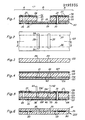
- the circuit board 20 shown schematically in FIG. 1 has rigid parts A and flexible parts B, the latter of which only a single one can be seen in FIG. 1.
- the printed circuit board 20 is composed of a plurality of layers arranged one above the other and connected to one another, as follows: A flexible insulating material layer 21 is connected by means of an adhesive layer 22 to a rigid insulating material layer 23, which only partially, namely on the rigid parts A, the flexible insulating material layer 21 the printed circuit board covered.
- the side of the flexible insulating material layer 21 facing away from the rigid insulating material layer 23 carries electrical conductor tracks 24 and a covering layer 25 made of insulating material and covers the latter.
- the printed circuit board 20 is also provided with through bores 29 and 30 which are assigned to the conductor tracks 27 and 24 and 27, respectively.
- individual conductor tracks 24 of the flexible layer 21 and individual conductor tracks 27 of the rigid layer 23 can be electrically conductively connected to one another by metallic plating 31 of the peripheral wall of the bores 30.
- the plate 123 prepared in this way is covered on one side according to FIG. 4 with an adhesive film 122 and a flexible insulating material film 121, which in turn is laminated with a copper film 124.
- the adhesive film 122 is cut out at the locations of the future flexible parts B of the printed circuit board to be produced, and a piece of separating film 40 of the same thickness which is cut to size is inserted into each of the recesses in the adhesive film 121 thus formed.
- a dimensionally stable adhesive film 126 and a copper film 127 are arranged on the opposite side of the plate 123.
- the flexible insulating material film 121, its copper cladding 124, the dimensionally stable adhesive film 126 and the copper film 127 run over the slots 33 of the rigid plate 124.
- the flexible foil 121 is then firmly connected to the rigid plate 123 by means of the adhesive foil 122 and the copper foil 127 by means of the non-flowing adhesive foil 126, the slots 33 of the plate 123 being hermetically sealed.
- the desired conductor tracks 24 and 27 are formed in a conventional manner from the copper foils 124 and 127 in a photo-chemical way. Then the holes 29 and 30 assigned to the conductor tracks are produced and - if necessary - the through-plating 31 is formed in a galvanic way. In all of these operations, the slots 33 of the plate 123 are protected against the ingress of foreign substances, in particular etching solution and electrolyte.
- cover sheets 125 and 128 are subsequently made of insulating mat over the finished conductor tracks 24 and 27 laminated rial, which are each coated on their side facing the conductor tracks with an adhesive (not shown).
- an adhesive not shown.
- the contour cuts of the printed circuit board 20 along the intended contour lines 36 and 37 (FIG. 2), the ends 34 and 35 of the slots 33 of the plate 123 being cut off.
- the cover film 128 and the dimensionally stable adhesive film 126 are cut along the slots 33, specifically at the future transition points between the rigid parts A and the flexible parts Areas B of the circuit board to be produced, as shown in FIG. 5.
- the copper foil 127 is omitted in the process phase shown in FIG. 4, so that the insulating material foil 126 alone then the slots 33 of the rigid plate 123 covers and prevents the penetration of foreign matter into the slots 33 during further processing of the circuit board.
- the printed circuit board is to have electrical conductor tracks lying in more than two planes, this can be achieved in that instead of the quasi-homogeneous rigid plate 123 according to FIG. 3, a layered plate 223 according to FIG. 6 is used, which has at least two rigid insulating material layers 50 and 51 and conductor tracks 53 arranged between them.
- the two rigid insulating material layers 50 and 51 are connected to one another by a dimensionally stable adhesive layer 54, in which the conductor tracks 53 are embedded.
- the plate 223 could have an even greater number of rigid insulating material layers and conductor tracks and adhesive layers arranged between them.
- the layered rigid board 223 is provided with slots 33 in exactly the same way and is used further as described with reference to the quasi-homogeneous board 123.
- Flexible insulating material foils 161 and 162 for example made of polyimide, which are each laminated with a copper foil on at least one of their flat sides, are used to produce the. electrical conductor tracks 64 and 65 processed in a conventional manner, after which a cover film 166 or 167 made of insulation is placed over the conductor tracks of each flexible film 161 or 162 Laminated material, which is coated on its side facing the conductor tracks with an adhesive (not shown).
- two adhesive films 168 and 169 made of modified epoxy resin are pre-processed in such a way that they are cut out at the locations of the future flexible parts B of the printed circuit board 60 to be produced.
- the sandwich-like layering shown in Fig. 9 is formed. From bottom to top, this contains: A dimensionally stable adhesive film 172 which carries a laminated copper film 174 on its downward-facing side; the first rigid plate 170 provided with slots 33; the adhesive film 168, which is cut out at the locations of the future flexible parts B of the printed circuit board, a separating film piece 80 of the same thickness being inserted into each recess of the adhesive film 168; the flexible insulating material film 161 provided with the conductor tracks 64 and the cover film 166; a cover film 163 of insulating material coated on both sides with adhesive; the flexible insulating material film 162 provided with the conductor tracks 68 and the cover film 167; the adhesive film 169, which is cut out at the locations of the future flexible parts B of the printed circuit board, a separating film piece 81 of the same thickness being inserted into each recess of the adhesive film 169; the second rigid plate 171 provided with slots 33, the slots 33 of both plates 170 and 171 having
- the desired outer conductor tracks 74 and 75 are subsequently produced from the outer copper foils 174 and 175 in the usual way by photo-chemical means. Then the holes 78 assigned to the conductor tracks and, if appropriate, the through-plating 79 are formed in a galvanic manner. In these photo-chemical and galvanic processing, the slots 33 of the plates 170 and 171 are protected against the penetration of etching solution and electrolyte.
- cover foils 176 and 177 made of insulating material are laminated over the finished outer conductor tracks 74 and 75, which are each coated with an adhesive (not shown) on their side facing the conductor tracks.
- the contour cuts of the printed circuit board 60 then follow along the contours 36 and 37 provided (FIG. 8), the ends 34 and 35 of the slots 33 of the two flaps 170 and 171 being cut off.
- the cover films 176 and 177 and the dimensionally stable adhesive films 172 and 173 are cut along the slots 33 with one or more cutting tools 41 and 42 on both outer sides. specifically at the future transition points between the rigid parts A and the flexible parts B of the printed circuit board 60 to be produced, as shown in FIG. 10.
- the plates and foils used for the production of the circuit board 60 expediently have approximately the same technological properties and thickness dimensions as were described with reference to the first exemplary embodiment.
- the printed circuit board it is possible and indicated for some uses of the printed circuit board to use a layered plate instead of at least one of the quasi-homogeneous rigid plates 170 and 171, as was described, for example, with reference to FIG. 6. It is also possible to arrange more than two flexible foils between the rigid plates, each carrying electrical conductor tracks on at least one side.
- the production processes described have the following main advantages over known processes for producing rigid and flexible sections of printed circuit boards: At the transition points between rigid sections A and flexible sections B of the printed circuit board, the rigid layers 23 and 70 and 71 have a smooth, clean and, above all fiber-free cut surfaces, which are formed by the slots 33. During the processing of the outer copper foils 124, 127 and 174, 175, the slots 33 of the rigid plate 123 and 223 or 170 and 171 are hermetically covered, so that the penetration of foreign substances such as Aetzlösurg or electrolyte is prevented.
- the parts 123 ', 126', 128 'or 170', 171 ', 172', 173 ', 176', 177 'covering the future flexible parts B are removed by simply cutting along the transition points between rigid and flexible parts of the printed circuit board ; there is no need for deep milling or breaking out. All steps of the manufacturing process can be carried out by the PCB manufacturer.
Landscapes
- Engineering & Computer Science (AREA)
- Microelectronics & Electronic Packaging (AREA)
- Manufacturing & Machinery (AREA)
- Physics & Mathematics (AREA)
- Electromagnetism (AREA)
- Production Of Multi-Layered Print Wiring Board (AREA)
- Structure Of Printed Boards (AREA)
Applications Claiming Priority (2)
| Application Number | Priority Date | Filing Date | Title |
|---|---|---|---|
| CH133285A CH667359A5 (de) | 1985-03-27 | 1985-03-27 | Verfahren zur herstellung einer starre und flexible partien aufweisenden leiterplatte fuer gedruckte elektrische schaltungen. |
| CH1332/85 | 1985-03-27 |
Publications (2)
| Publication Number | Publication Date |
|---|---|
| EP0195935A2 true EP0195935A2 (fr) | 1986-10-01 |
| EP0195935A3 EP0195935A3 (fr) | 1987-06-03 |
Family
ID=4207993
Family Applications (1)
| Application Number | Title | Priority Date | Filing Date |
|---|---|---|---|
| EP86102244A Withdrawn EP0195935A3 (fr) | 1985-03-27 | 1986-02-20 | Procédé de fabrication d'un substrat comportant des parties rigides et flexibles pour circuits imprimés |
Country Status (2)
| Country | Link |
|---|---|
| EP (1) | EP0195935A3 (fr) |
| CH (1) | CH667359A5 (fr) |
Cited By (15)
| Publication number | Priority date | Publication date | Assignee | Title |
|---|---|---|---|---|
| GB2207288A (en) * | 1987-06-30 | 1989-01-25 | Nippon Mektron Kk | A method of producing a hybrid multi-layered circuit substrate |
| US5144742A (en) * | 1991-02-27 | 1992-09-08 | Zycon Corporation | Method of making rigid-flex printed circuit boards |
| EP0540640A4 (en) * | 1990-07-24 | 1993-06-30 | Miraco, Inc. | Combined rigid and flexible printed circuits |
| WO2008098270A1 (fr) * | 2007-02-16 | 2008-08-21 | At & S Austria Technologie & Systemtechnik Aktiengesellschaft | Procédé de fabrication d'une carte de circuits imprimés flexo-rigide et carte de circuits imprimés flexo-rigide |
| EP2020833A1 (fr) * | 2007-07-31 | 2009-02-04 | Beauce Réalisations et Études Électroniques (BREE) | Procédé de fabrication d'un circuit imprimé semi-flexible, plaque utilisée pour un tel procédé, circuit imprimé et dispositif électronique associés |
| EP1881749A3 (fr) * | 2006-07-20 | 2010-04-07 | Dyconex AG | Procédé de fabrication d'un élément de connexion électrique, et élément de connexion électrique |
| AT13434U1 (de) * | 2012-02-21 | 2013-12-15 | Austria Tech & System Tech | Verfahren zur Herstellung einer Leiterplatte und Verwendung eines derartigen Verfahrens |
| WO2014100848A1 (fr) * | 2012-12-31 | 2014-07-03 | At&S Austria Technologie & Systemtechnik Aktiengesellschaft | Produit semi-fini servant à la production d'une carte de circuit imprimé et procédé de production afférent |
| CN105682384A (zh) * | 2016-04-01 | 2016-06-15 | 信利电子有限公司 | 一种柔性多层线路板及其制作方法 |
| WO2017025542A1 (fr) * | 2015-08-12 | 2017-02-16 | Schweizer Electronic Ag | Antenne à haute frequence, substrat à haute frequence comprenant une antenne à haute frequence et procédé de production |
| WO2017025552A1 (fr) * | 2015-08-12 | 2017-02-16 | Schweizer Electronic Ag | Élément à structure conductrice avec substrat de couche intérieure laminé et son procédé de fabrication |
| US10187997B2 (en) | 2014-02-27 | 2019-01-22 | At&S Austria Technologie & Systemtechnik Aktiengesellschaft | Method for making contact with a component embedded in a printed circuit board |
| US10219384B2 (en) | 2013-11-27 | 2019-02-26 | At&S Austria Technologie & Systemtechnik Aktiengesellschaft | Circuit board structure |
| US10779413B2 (en) | 2013-12-12 | 2020-09-15 | At&S Austria Technologie & Systemtechnik Aktiengesellschaft | Method of embedding a component in a printed circuit board |
| US11523520B2 (en) | 2014-02-27 | 2022-12-06 | At&S Austria Technologie & Systemtechnik Aktiengesellschaft | Method for making contact with a component embedded in a printed circuit board |
Family Cites Families (6)
| Publication number | Priority date | Publication date | Assignee | Title |
|---|---|---|---|---|
| US3984290A (en) * | 1973-10-01 | 1976-10-05 | Georgy Avenirovich Kitaev | Method of forming intralayer junctions in a multilayer structure |
| DE2914336A1 (de) * | 1979-04-09 | 1980-11-06 | Telefonbau & Normalzeit Gmbh | Verfahren zur herstellung starr- flexibler leiterplatten |
| DE2946726C2 (de) * | 1979-11-20 | 1982-05-19 | Ruwel-Werke Spezialfabrik für Leiterplatten GmbH, 4170 Geldern | Leiterplatte mit starren und flexiblen Bereichen und Verfahren zu deren Herstellung |
| DE3047197C1 (de) * | 1980-12-15 | 1982-05-27 | Siemens AG, 1000 Berlin und 8000 München | Verfahren zur Herstellung von Leiterplatten,die abschnittsweise relativ starre und demgegenueber relativ flexible Bereiche aufweisen |
| DE3119884C1 (de) * | 1981-05-19 | 1982-11-04 | Fritz Wittig Herstellung gedruckter Schaltungen, 8000 München | Verfahren zur Herstellung von starre und flexible Bereiche aufweisenden Leiterplatten |
| DE3515549A1 (de) * | 1985-04-30 | 1986-10-30 | El.M.Te. Gesellschaft für Elektronik und Messtechnik Höller mbH & Co KG, 8302 Mainburg | Verfahren zur herstellung von leiterplatten |
-
1985
- 1985-03-27 CH CH133285A patent/CH667359A5/de not_active IP Right Cessation
-
1986
- 1986-02-20 EP EP86102244A patent/EP0195935A3/fr not_active Withdrawn
Cited By (24)
| Publication number | Priority date | Publication date | Assignee | Title |
|---|---|---|---|---|
| GB2207288A (en) * | 1987-06-30 | 1989-01-25 | Nippon Mektron Kk | A method of producing a hybrid multi-layered circuit substrate |
| GB2207288B (en) * | 1987-06-30 | 1991-09-11 | Nippon Mektron Kk | An improved method of producing a hybrid multi-layered circuit substrate |
| EP0540640A4 (en) * | 1990-07-24 | 1993-06-30 | Miraco, Inc. | Combined rigid and flexible printed circuits |
| US5144742A (en) * | 1991-02-27 | 1992-09-08 | Zycon Corporation | Method of making rigid-flex printed circuit boards |
| US7892625B2 (en) | 2006-07-20 | 2011-02-22 | Dyconex Ag | Method of fabricating an electrical connecting element, and an electrical connecting element |
| EP1881749A3 (fr) * | 2006-07-20 | 2010-04-07 | Dyconex AG | Procédé de fabrication d'un élément de connexion électrique, et élément de connexion électrique |
| WO2008098270A1 (fr) * | 2007-02-16 | 2008-08-21 | At & S Austria Technologie & Systemtechnik Aktiengesellschaft | Procédé de fabrication d'une carte de circuits imprimés flexo-rigide et carte de circuits imprimés flexo-rigide |
| FR2919781A1 (fr) * | 2007-07-31 | 2009-02-06 | Beauce Realisations Et Etudes | Procede de fabrication d'un circuit imprime semi-flexible, plaque utilisee pour un tel procede, circuit imprime et dispositif electronique associes |
| EP2020833A1 (fr) * | 2007-07-31 | 2009-02-04 | Beauce Réalisations et Études Électroniques (BREE) | Procédé de fabrication d'un circuit imprimé semi-flexible, plaque utilisée pour un tel procédé, circuit imprimé et dispositif électronique associés |
| AT13434U1 (de) * | 2012-02-21 | 2013-12-15 | Austria Tech & System Tech | Verfahren zur Herstellung einer Leiterplatte und Verwendung eines derartigen Verfahrens |
| US9820381B2 (en) | 2012-12-31 | 2017-11-14 | AT&S Austria Technologie Systemtechnik Aktiengesellschaft | Semi-finished product for the production of a printed circuit board and method for producing the same |
| WO2014100848A1 (fr) * | 2012-12-31 | 2014-07-03 | At&S Austria Technologie & Systemtechnik Aktiengesellschaft | Produit semi-fini servant à la production d'une carte de circuit imprimé et procédé de production afférent |
| US11172576B2 (en) | 2013-11-27 | 2021-11-09 | At&S Austria Technologie & Systemtechnik Aktiengesellschaft | Method for producing a printed circuit board structure |
| US10219384B2 (en) | 2013-11-27 | 2019-02-26 | At&S Austria Technologie & Systemtechnik Aktiengesellschaft | Circuit board structure |
| US10779413B2 (en) | 2013-12-12 | 2020-09-15 | At&S Austria Technologie & Systemtechnik Aktiengesellschaft | Method of embedding a component in a printed circuit board |
| US10187997B2 (en) | 2014-02-27 | 2019-01-22 | At&S Austria Technologie & Systemtechnik Aktiengesellschaft | Method for making contact with a component embedded in a printed circuit board |
| US11523520B2 (en) | 2014-02-27 | 2022-12-06 | At&S Austria Technologie & Systemtechnik Aktiengesellschaft | Method for making contact with a component embedded in a printed circuit board |
| US12185478B2 (en) | 2014-02-27 | 2024-12-31 | At&S Austria Technologie & Systemtechnik Aktiengesellschaft | Printed circuit board having embedded component |
| WO2017025542A1 (fr) * | 2015-08-12 | 2017-02-16 | Schweizer Electronic Ag | Antenne à haute frequence, substrat à haute frequence comprenant une antenne à haute frequence et procédé de production |
| US10602606B2 (en) | 2015-08-12 | 2020-03-24 | Schweizer Electronic Ag | Radio-frequency antenna, radio-frequency substrate with radio-frequency antenna, and production method |
| US10555419B2 (en) | 2015-08-12 | 2020-02-04 | Schweizer Electronic Ag | Conductor-structure element having an internal layer substrate laminated into same, and method for the production thereof |
| WO2017025552A1 (fr) * | 2015-08-12 | 2017-02-16 | Schweizer Electronic Ag | Élément à structure conductrice avec substrat de couche intérieure laminé et son procédé de fabrication |
| CN105682384B (zh) * | 2016-04-01 | 2019-04-26 | 信利电子有限公司 | 一种柔性多层线路板及其制作方法 |
| CN105682384A (zh) * | 2016-04-01 | 2016-06-15 | 信利电子有限公司 | 一种柔性多层线路板及其制作方法 |
Also Published As
| Publication number | Publication date |
|---|---|
| CH667359A5 (de) | 1988-09-30 |
| EP0195935A3 (fr) | 1987-06-03 |
Similar Documents
| Publication | Publication Date | Title |
|---|---|---|
| DE2702844C2 (de) | Verfahren zur Herstellung einer vielschichtigen gedruckten Schaltung | |
| DE4006063C2 (de) | Verfahren zur Herstellung einer Leiterplatte | |
| DE69117381T2 (de) | Mehrschichtleiterplatte und Verfahren zu ihrer Herstellung | |
| DE68920607T2 (de) | Verfahren zum Aufbau einer Leiterplatten-Anordnung von hoher Leistungsfähigkeit. | |
| DE69319283T2 (de) | Metallträger für ein Mehrschicht-Leitergitter und Verfahren zum Herstellen desselben | |
| DE69218119T2 (de) | Vorrichtung mit flexiblen streifenleitern und verfahren zur herstellung einer derartigen vorrichtung | |
| EP0175045A2 (fr) | Méthode pour la production de plaquettes à circuit imprimé flexibles pour grand effort de flexion à connexions traversantes | |
| EP0195935A2 (fr) | Procédé de fabrication d'un substrat comportant des parties rigides et flexibles pour circuits imprimés | |
| DE4100233A1 (de) | Verfahren zum herstellen gedruckter schaltungen | |
| EP0408773B1 (fr) | Procédé pour la fabrication de plaques à circuits ou de couches internes de plaques à circuit contenant des parties rigides et flexibles | |
| DE2447284A1 (de) | Verfahren zum aufbringen einer gleichmaessigen goldplattierung an keramischen substraten | |
| EP0080756A1 (fr) | Plaquette de circuit comportant des zones rigides et felxibles et son procédé de fabrication | |
| DE19615395A1 (de) | Elektrostatische Schutzvorrichtung und Verfahren zu ihrer Herstellung | |
| EP0700630B1 (fr) | Carte a circuit imprime en feuille mince et procede de fabrication | |
| DE4020498C2 (de) | Verfahren zum Herstellen von Multiwire-Leiterplatten mit isolierten Metalleitern und/oder optischen Leitern | |
| WO2015077808A1 (fr) | Structure de carte de circuits imprimés | |
| EP1550358A2 (fr) | Carte de circuit imprime presentant au moins une partie rigide et une partie souple et procede de production de cartes de circuits imprimes rigides et souples | |
| DE69318937T2 (de) | Mehrschicht Leiterrahmen für eine Halbleiteranordnung | |
| DE102018203715A1 (de) | Verfahren zur Herstellung einer Leiterplatte unter Verwendung einer Form für Leiterelemente | |
| DE4208610C1 (en) | Rigid-flexible PCB with flexible circuit foil mfg. - having flexible PCB in flexible region with fracture lines in rigid outer layers along rigid-flexible transition allowing rigid part to be removed along fracture lines after processing | |
| WO2004030429A1 (fr) | Procede de production de cartes imprimees flexo-rigides et carte imprimee comprenant au moins une zone rigide et au moins une zone flexible | |
| EP0710432B1 (fr) | Procede de fabrication de circuits imprimes en feuilles ou de produits semi-finis destines a la fabrication de circuits imprimes en feuilles, ainsi que circuits imprimes en feuilles et produits semi-finis fabriques selon ce procede | |
| DE19627543A1 (de) | Multi-Layer-Substrat sowie Verfahren zu seiner Herstellung | |
| DE3931551A1 (de) | Verfahren zum herstellen eines mehrschichtigen, kupfer- und keramikschichten aufweisenden substrates | |
| WO2012167937A2 (fr) | Procédé de fabrication de cartes de circuits imprimés et utilisation intégrale de cartes de circuits imprimés |
Legal Events
| Date | Code | Title | Description |
|---|---|---|---|
| PUAI | Public reference made under article 153(3) epc to a published international application that has entered the european phase |
Free format text: ORIGINAL CODE: 0009012 |
|
| AK | Designated contracting states |
Kind code of ref document: A2 Designated state(s): AT BE CH DE FR GB IT LI LU NL SE |
|
| ITCL | It: translation for ep claims filed |
Representative=s name: ING. A. GIAMBROCONO & C. S.R.L. |
|
| TCNL | Nl: translation of patent claims filed | ||
| EL | Fr: translation of claims filed | ||
| PUAL | Search report despatched |
Free format text: ORIGINAL CODE: 0009013 |
|
| AK | Designated contracting states |
Kind code of ref document: A3 Designated state(s): AT BE CH DE FR GB IT LI LU NL SE |
|
| STAA | Information on the status of an ep patent application or granted ep patent |
Free format text: STATUS: THE APPLICATION IS DEEMED TO BE WITHDRAWN |
|
| 18D | Application deemed to be withdrawn |
Effective date: 19871204 |
|
| RIN1 | Information on inventor provided before grant (corrected) |
Inventor name: SIMM, IVAR CHRISTOF |