EP0196098A2 - Amplificateur/mélangeur à large bande - Google Patents
Amplificateur/mélangeur à large bande Download PDFInfo
- Publication number
- EP0196098A2 EP0196098A2 EP86104236A EP86104236A EP0196098A2 EP 0196098 A2 EP0196098 A2 EP 0196098A2 EP 86104236 A EP86104236 A EP 86104236A EP 86104236 A EP86104236 A EP 86104236A EP 0196098 A2 EP0196098 A2 EP 0196098A2
- Authority
- EP
- European Patent Office
- Prior art keywords
- transmission line
- fets
- line means
- circuit
- mixer
- Prior art date
- Legal status (The legal status is an assumption and is not a legal conclusion. Google has not performed a legal analysis and makes no representation as to the accuracy of the status listed.)
- Granted
Links
Images

Classifications
-
- H—ELECTRICITY
- H03—ELECTRONIC CIRCUITRY
- H03F—AMPLIFIERS
- H03F3/00—Amplifiers with only discharge tubes or only semiconductor devices as amplifying elements
- H03F3/60—Amplifiers in which coupling networks have distributed constants, e.g. with waveguide resonators
- H03F3/605—Distributed amplifiers
- H03F3/607—Distributed amplifiers using FET's
-
- H—ELECTRICITY
- H03—ELECTRONIC CIRCUITRY
- H03D—DEMODULATION OR TRANSFERENCE OF MODULATION FROM ONE CARRIER TO ANOTHER
- H03D7/00—Transference of modulation from one carrier to another, e.g. frequency-changing
- H03D7/14—Balanced arrangements
- H03D7/1425—Balanced arrangements with transistors
- H03D7/1441—Balanced arrangements with transistors using field-effect transistors
-
- H—ELECTRICITY
- H03—ELECTRONIC CIRCUITRY
- H03D—DEMODULATION OR TRANSFERENCE OF MODULATION FROM ONE CARRIER TO ANOTHER
- H03D7/00—Transference of modulation from one carrier to another, e.g. frequency-changing
- H03D7/14—Balanced arrangements
- H03D7/1425—Balanced arrangements with transistors
- H03D7/1458—Double balanced arrangements, i.e. where both input signals are differential
-
- H—ELECTRICITY
- H03—ELECTRONIC CIRCUITRY
- H03D—DEMODULATION OR TRANSFERENCE OF MODULATION FROM ONE CARRIER TO ANOTHER
- H03D9/00—Demodulation or transference of modulation of modulated electromagnetic waves
- H03D9/06—Transference of modulation using distributed inductance and capacitance
- H03D9/0658—Transference of modulation using distributed inductance and capacitance by means of semiconductor devices having more than two electrodes
- H03D9/0675—Transference of modulation using distributed inductance and capacitance by means of semiconductor devices having more than two electrodes using field effect transistors
-
- H—ELECTRICITY
- H03—ELECTRONIC CIRCUITRY
- H03D—DEMODULATION OR TRANSFERENCE OF MODULATION FROM ONE CARRIER TO ANOTHER
- H03D2200/00—Indexing scheme relating to details of demodulation or transference of modulation from one carrier to another covered by H03D
- H03D2200/0001—Circuit elements of demodulators
- H03D2200/0007—Dual gate field effect transistors
-
- H—ELECTRICITY
- H03—ELECTRONIC CIRCUITRY
- H03D—DEMODULATION OR TRANSFERENCE OF MODULATION FROM ONE CARRIER TO ANOTHER
- H03D2200/00—Indexing scheme relating to details of demodulation or transference of modulation from one carrier to another covered by H03D
- H03D2200/0001—Circuit elements of demodulators
- H03D2200/0011—Diodes
- H03D2200/0013—Diodes connected in a ring configuration
-
- H—ELECTRICITY
- H03—ELECTRONIC CIRCUITRY
- H03D—DEMODULATION OR TRANSFERENCE OF MODULATION FROM ONE CARRIER TO ANOTHER
- H03D2200/00—Indexing scheme relating to details of demodulation or transference of modulation from one carrier to another covered by H03D
- H03D2200/0001—Circuit elements of demodulators
- H03D2200/0023—Balun circuits
-
- H—ELECTRICITY
- H03—ELECTRONIC CIRCUITRY
- H03D—DEMODULATION OR TRANSFERENCE OF MODULATION FROM ONE CARRIER TO ANOTHER
- H03D2200/00—Indexing scheme relating to details of demodulation or transference of modulation from one carrier to another covered by H03D
- H03D2200/0041—Functional aspects of demodulators
- H03D2200/0066—Mixing
- H03D2200/0076—Mixing using a distributed mixer
-
- H—ELECTRICITY
- H03—ELECTRONIC CIRCUITRY
- H03D—DEMODULATION OR TRANSFERENCE OF MODULATION FROM ONE CARRIER TO ANOTHER
- H03D7/00—Transference of modulation from one carrier to another, e.g. frequency-changing
- H03D7/12—Transference of modulation from one carrier to another, e.g. frequency-changing by means of semiconductor devices having more than two electrodes
- H03D7/125—Transference of modulation from one carrier to another, e.g. frequency-changing by means of semiconductor devices having more than two electrodes with field effect transistors
-
- H—ELECTRICITY
- H03—ELECTRONIC CIRCUITRY
- H03D—DEMODULATION OR TRANSFERENCE OF MODULATION FROM ONE CARRIER TO ANOTHER
- H03D9/00—Demodulation or transference of modulation of modulated electromagnetic waves
- H03D9/06—Transference of modulation using distributed inductance and capacitance
- H03D9/0658—Transference of modulation using distributed inductance and capacitance by means of semiconductor devices having more than two electrodes
Definitions
- the present invention relates to a broadband distributed amplifier/mixer according to the preamble of claim 1.
- the invention is used in the art of high frequency (>1GHz) multi-octave distributed amplifier driver and combiner circuitry with gain to accomplish wideband frequency mixing.
- High frequency wide bandwidth monolithic distributed circuits have been known in the art for applications mainly as broadband microwave amplifiers.
- the inventive circuitry is compatible with GaAs monolithic integration and applicable to microwave and mm-wave systems.
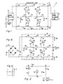
- a high frequency, (for example, 2-60GHz) broadband mixer circuit 10 which has very generally a mixer element 11, a paraphase dual distributed amplifier 12, an input signal splitter 13, a local oscillator 14, an RF input port 15, a broadband distributed combiner 16 and an IF output port 17.
- the signal splitter 13 receives the signal from the local oscillator, splits the signal and delivers it in the same phase to input terminals 20 and 21 of the transmission line formed by the outboard series inductances and shunt capacitances of the broadband paraphase distributed amplifier 12.
- the signal splitter may be a resistive network like that shown in Figure la.
- Dual distributed amplifier 12 is represented by the schematic as having two pairs of FETs but the number of cascaded pairs may vary as necessary.
- Input terminal 20 is shown connected through series inductive segments 22, 23 and 24 to amplifier output terminal 25.
- input terminal 21 is connected through series inductive segments 32, 33 and 34 to amplifier output terminal 35.
- RF input terminal 15 is connected through series inductive segments 42, 43 and 44 and a resistive element 45 to ground.
- Between segments 22 and 23 is a junction 26, and between segments 23 and 24 is a junction 27.
- Between segments 32 and 33 is a junction 36, and between segments 33 and 34 is a junction 37.
- Junctions 46 and 47 are similarly located intermediate the inductive elements 42, 43 and 44.
- a first FET 50 has its drain connected to junction 26, its source connected to ground, and its gate connected to junction 46.
- FET 50 is paired with FET 51 which has its source connected to junction 46, its drain to junction 36, and its gate connected to ground.
- FET 52 has its drain connected to junction 27, its source to ground, and its gate to junction 47.
- FET 53 which has its source connected to junction 47, its drain to junction 37, and its gate connected to ground.
- the FETs 51 and 53, the inductive segments 32, 33 and 34, the common RF inductive segments 42, 43 and 44 and the associated capacitive effects comprise the second half of the dual distributed amplifier.
- the output terminals 25 and 35 of the dual distributed amplifier are connected to the input terminals 54 and 55 of mixer element 11.
- the present mixer is conventional in the sense of converting RP energy at one frequency into energy at another frequency 'to make the signal processing easier.
- Mixers have been conventionally classified as single-ended, single-balanced, double-balanced, and double double-balanced to name several.
- An example of a double-balanced mixer shown in Figure lb is the ring modulator 11' which has output terminals 56 and 57. Terminals 56 and 57 are connected to the inputs of broadband distributed combiner 16. Terminal 56 is shown connected through series inductive segments 62, 63 and 64 and resistor 65 to ground. Terminal 57 is shown connected through series inductive segments 72, 73 and 74 and resistor 75 to ground.
- a common central leg terminating at IF output 17 can be traced from ground through resistor 85, and series inductive segments 82, 83 and 84.
- Between elements 62 and 63 is a junction 66; between elements 63 and 64 is a junction 67; between elements 72 and 73 is a junction 76; between elements 73 and 74 is a junction 77; between elements 82 and 83 is a junction 86 and between elements 83 and 84 is a junction 87.
- a FET 90 has its source connected to junction 66, its drain connected to junction 86 and its. gate connected to ground. It is paired with FET 91 which has its drain connected to junction 86, its gate connected to junction 76, and its source connected to ground.
- FET 92 has its source connected to junction 67, its drain connected to junction 87 and its gate connected to ground. It is paired with FET 93 which has its drain connected to junction 87, its gate connected to junction 77 and its source connected to ground.
- FETs 90 and 92, the inductive segments 62, 63 and 64, the common inductive segments 82, 83 and 84 and the associated distributed capacity including the FET capacity shown in Figure 2 comprise the first half of the distributed combiner 16.
- the FETs 91 and 93, the inductive.segments 72, 73 and 74, the common inductive segments 82, 83 and 84 and the associated distributed capacity comprise the second half of the dual distributed signal combiner.
- FIG. 2 shows a simplified equivalent circuit of the MESFETs operating at the high frequencies (>lG H z) described herein.
- the capacitance gate-to-source, Cgs forms a major part of the input transmission line capacitance
- the capacitance drain-to-source, Cds forms a major part of the output transmission line capacitance.
- Cdg is the drain to gate capacitance
- g m is the transconductance
- i dc represents the voltage dependent current generator function of the'FET.
- the transistor pairs are cross bonded with each other which means the source electrode of each FET is connected to the gate of the other.
- the same signal is fed to the drain of each of FETs 50 and 51 from the oscillator 14 while the RF signal causes opposite effects in the conductivity of FET 50 versus FET 51, for example.
- FET pair 52 and 53 is controlled in similar fashion.
- the distributed combiner 16 of Figure lb a similar circuit configuration exists and the opposite signals on input terminals 56 and 57 combine at the FET pairs to provide a single IF output at 17.
- the mixer itself is the non-linear element shown in block diagram 11 in Figure 1, and in a representative schematic form 11' in Figure lb.
- this mixer element is driven by a passive transformer (balun) and the output at IF is likewise combined in a passive transformer.
- the transformers are replaced by distributed amplifiers which provide conversion gain.
- the driver is a distributed paraphase amplifier which allows the RF signal to be applied to the mixer element in push-pull.
- the paraphase output transmission lines are driven by a local oscillator signal which provides a push-push drive to the mixer element.
- FIG. 3 there is disclosed another embodiment of the broadband monolithic dual distributed amplifier/mixer.
- the RF signal 100 is connected through an in-phase signal splitter 101 to RF input terminals 102 and 103 of the dual distributed amplifier/mixer generally shown at 104.
- the opposite ends of the transmission lines include input terminals 105 and 106 which are fed through a paraphase splitter 107 from a local oscillator 108.
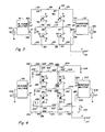
- Both of the signal splitters can be active monolithic circuits using distributed circuit concepts as shown in Figures 5 and 6.
- a transmission line circuit 120 can be traced from terminal 102 through an inductive segment 122, a junction 126, an inductive segment 123, a junction 127, and an inductive segment 124 to the terminal 105.
- a similar circuit 130 can be traced from terminal 103 through an inductive segment 132, a junction 136, an inductive segment 133, a junction 137, and an inductive segment 134 to the terminal 106.
- a third common IF transmission line circuit 140 can be traced from ground through a resistive element 141, an inductive segment 142, a junction 146, an inductive segment 143, a junction 147, and an inductive segment 144 to IF output terminal 117.
- FETs 150, 151, 152 and 153 have grounded source electrodes.
- FET 150 has its gate connected to junction 126 and its drain connected to 146.
- the gate of FET 151 is connected to junction 136 and its drain to 146.
- the gate of FET 152 is connected to junction 127 and its drain to 147.
- the gate of FET 153 connects to 137 and the drain to 147.
- the FETs 150 and 152, the inductive segments 122, 123 and 124, the inductive segments 142, 143 and 144 and the associated capacitive effects comprise the first half of the dual distributed amplifier/mixer.
- the FETs 151 and 153, the inductive segments 132, 133 and 134, the common inductive segments 142, 143 and 144 and the capacity effects comprise the second half of the dual distributed amplifier/mixer.
- the embodiment of this Figure also provides conversion gain.
- a modification of the monolithic mixer of Figure 3 is shown in Figure 4 in which dual gate FETs 250, 251, 252 and 253 are used in place of the single gate FETs of Figure 3.
- Separate transmission line portions 220 and 220', 230 and 230' are shown in Figure 4 and will be explained, otherwise the circuit is similar to that explained in Figure 3.
- a transmission line circuit 220 can be traced from in-phase splitter 201 through terminal 202, inductive segment 222, junction 226, inductive segment 223, junction 227, inductive segment 224 and resistor 225 to ground.
- a transmission line circuit 220' can be traced from paraphase splitter 207 through terminal 205, inductive segment 224', junction 227' and resistor 225' to ground.
- Gate Gl and G2 of FET 250 are connected to junctions 226 and 226', respecitvely.
- Gate Gl and G2 of FET 252 are connected to junctions 227 and 227', respectively.
- a transmission line circuit 230 can be traced from splitter 201 through terminal 203, inductive segment 232, junction 236, inductive segment 233, junction 237, inductive segment 234 and resistor 235 to ground.
- a transmission line circuit 230' can be traced from paraphase splitter 207 through terminal 206, inductive segment 234', junction 237', inductive segment 233', junction 236', inductive segment 232' and resistor 235' to ground.
- Gates Gl and G2 of FET 251 are connected to juntions 236 and 236' respectively.
- Gates Gl and G2 of FET 253 are connected to junctions 237 and 237' respectively.
- IF output transmission line circuit 240 can be traced from ground through resistor 241, an inductive segment 242, a junction 246, an inductive segment 243, a junction 247, and an inductive segment 244 to IF output terminal 217.
- FETs 250 and 251 each has its drain connected to junction 246 and FETs 252 and 253 each has its drain connected to junction 247.
- the source electrodes of each of the four FETs is qrounded.
- FIGS. 3 and 4 show a broadband mixer circuit with conversion gain which utilizes either single gate FETs 150, 151, 152 and 153 in Figure 3 or dual gate FETs 250, 251, 252 and 253 in Figure 4 for the mixing elements.
- the active splitters as well as the FETs used for mixing are realized as distributed amplifiers shown in Figures 5 and 6.
- the paraphase splitter and the in-phase splitter provides, respectively, push-pull and push-push signals of the RF signal and the local oscillator signal to drive the mixer FETs.
- the entire circuit is compatible for monolithic integration.
- the mixer 11, 11' which is there shown in a ring modulator form, may also be an active distributed mixer.
Landscapes
- Engineering & Computer Science (AREA)
- Power Engineering (AREA)
- Physics & Mathematics (AREA)
- Electromagnetism (AREA)
- Microwave Amplifiers (AREA)
- Amplifiers (AREA)
Applications Claiming Priority (2)
| Application Number | Priority Date | Filing Date | Title |
|---|---|---|---|
| US71791885A | 1985-03-29 | 1985-03-29 | |
| US717918 | 1985-03-29 |
Publications (3)
| Publication Number | Publication Date |
|---|---|
| EP0196098A2 true EP0196098A2 (fr) | 1986-10-01 |
| EP0196098A3 EP0196098A3 (en) | 1988-07-13 |
| EP0196098B1 EP0196098B1 (fr) | 1992-05-20 |
Family
ID=24884030
Family Applications (1)
| Application Number | Title | Priority Date | Filing Date |
|---|---|---|---|
| EP86104236A Expired EP0196098B1 (fr) | 1985-03-29 | 1986-03-27 | Amplificateur/mélangeur à large bande |
Country Status (3)
| Country | Link |
|---|---|
| EP (1) | EP0196098B1 (fr) |
| JP (1) | JPH0680984B2 (fr) |
| DE (1) | DE3685355D1 (fr) |
Cited By (9)
| Publication number | Priority date | Publication date | Assignee | Title |
|---|---|---|---|---|
| US4751744A (en) * | 1985-05-28 | 1988-06-14 | Texas Instruments Incorporated | Monolithic distributed mixer |
| EP0266198A3 (fr) * | 1986-10-31 | 1989-08-23 | Texas Instruments Incorporated | Multiplicateur de fréquence équilibré distribué |
| EP0340713A1 (fr) * | 1988-05-04 | 1989-11-08 | Alcatel Cit | Dispositif de distribution de signaux numeriques a tres hauts debits |
| GB2325102A (en) * | 1997-05-09 | 1998-11-11 | Nokia Mobile Phones Ltd | Down conversion mixer |
| US5880640A (en) * | 1989-11-24 | 1999-03-09 | Dassault Electronique | Distributed amplifier for wide band hyperfrequency signals |
| FR2795571A1 (fr) * | 1987-11-24 | 2000-12-29 | Dassault Electronique | Amplificateur de puissance a large bande en hyperfrequences |
| EP1732211A1 (fr) | 2005-06-08 | 2006-12-13 | Fujitsu Limited | Amplificateur distribué |
| EP1801968A1 (fr) | 2005-12-21 | 2007-06-27 | Thales | Structure de balun à large bande passante |
| CN108039870A (zh) * | 2018-01-08 | 2018-05-15 | 成都智芯测控科技有限公司 | 一种超宽带分布式混频器 |
Families Citing this family (5)
| Publication number | Priority date | Publication date | Assignee | Title |
|---|---|---|---|---|
| US4662000A (en) * | 1985-04-15 | 1987-04-28 | Raytheon Company | Frequency conversion circuits |
| US5136720A (en) * | 1989-11-30 | 1992-08-04 | Raytheon Company | Matrixed mixer |
| ATE391359T1 (de) * | 2003-12-10 | 2008-04-15 | Ericsson Telefon Ab L M | Mischervorrichtung |
| WO2013183097A1 (fr) * | 2012-06-08 | 2013-12-12 | 日本電気株式会社 | Amplificateur à répartition et module d'amplificateur l'utilisant |
| EP2944157B1 (fr) | 2013-01-08 | 2016-08-24 | Whoop Wireless LLC | Système et procédé permettant l'étalonnage d'un système d'amplificateur distribué |
Family Cites Families (2)
| Publication number | Priority date | Publication date | Assignee | Title |
|---|---|---|---|---|
| US3661443A (en) * | 1970-08-07 | 1972-05-09 | Us Air Force | 100 megahertz bandwidth modulator driver |
| US4446445A (en) * | 1982-11-24 | 1984-05-01 | Rockwell International Corporation | Singly terminated push-pull distributed amplifier |
-
1986
- 1986-03-27 EP EP86104236A patent/EP0196098B1/fr not_active Expired
- 1986-03-27 DE DE8686104236T patent/DE3685355D1/de not_active Expired - Fee Related
- 1986-03-28 JP JP61068870A patent/JPH0680984B2/ja not_active Expired - Lifetime
Cited By (14)
| Publication number | Priority date | Publication date | Assignee | Title |
|---|---|---|---|---|
| US4751744A (en) * | 1985-05-28 | 1988-06-14 | Texas Instruments Incorporated | Monolithic distributed mixer |
| EP0266198A3 (fr) * | 1986-10-31 | 1989-08-23 | Texas Instruments Incorporated | Multiplicateur de fréquence équilibré distribué |
| FR2795571A1 (fr) * | 1987-11-24 | 2000-12-29 | Dassault Electronique | Amplificateur de puissance a large bande en hyperfrequences |
| EP0340713A1 (fr) * | 1988-05-04 | 1989-11-08 | Alcatel Cit | Dispositif de distribution de signaux numeriques a tres hauts debits |
| FR2631169A1 (fr) * | 1988-05-04 | 1989-11-10 | Cit Alcatel | Dispositif de distribution de signaux numeriques a tres hauts debits |
| US4947144A (en) * | 1988-05-04 | 1990-08-07 | Alcatel N.V. | Distribution device for distributing very high data rate digital signals |
| US5880640A (en) * | 1989-11-24 | 1999-03-09 | Dassault Electronique | Distributed amplifier for wide band hyperfrequency signals |
| US6073001A (en) * | 1997-05-09 | 2000-06-06 | Nokia Mobile Phones Limited | Down conversion mixer |
| GB2325102A (en) * | 1997-05-09 | 1998-11-11 | Nokia Mobile Phones Ltd | Down conversion mixer |
| GB2325102B (en) * | 1997-05-09 | 2001-10-10 | Nokia Mobile Phones Ltd | Down conversion mixer |
| EP1732211A1 (fr) | 2005-06-08 | 2006-12-13 | Fujitsu Limited | Amplificateur distribué |
| US7804357B2 (en) | 2005-06-08 | 2010-09-28 | Fujitsu Limited | Distributed amplifier |
| EP1801968A1 (fr) | 2005-12-21 | 2007-06-27 | Thales | Structure de balun à large bande passante |
| CN108039870A (zh) * | 2018-01-08 | 2018-05-15 | 成都智芯测控科技有限公司 | 一种超宽带分布式混频器 |
Also Published As
| Publication number | Publication date |
|---|---|
| DE3685355D1 (de) | 1992-06-25 |
| EP0196098B1 (fr) | 1992-05-20 |
| EP0196098A3 (en) | 1988-07-13 |
| JPH0680984B2 (ja) | 1994-10-12 |
| JPS61270906A (ja) | 1986-12-01 |
Similar Documents
| Publication | Publication Date | Title |
|---|---|---|
| US4675911A (en) | Monolithic microwave integrated circuit broadband mixer | |
| US5060298A (en) | Monolithic double balanced mixer with high third order intercept point employing an active distributed balun | |
| US4896374A (en) | Broadband monolithic balanced mixer apparatus | |
| US5039891A (en) | Planar broadband FET balun | |
| US5274341A (en) | High-frequency power amplifier | |
| US6229395B1 (en) | Differential transconductance amplifier | |
| EP0196098A2 (fr) | Amplificateur/mélangeur à large bande | |
| US4611184A (en) | Microwave frequency power divider | |
| US4973918A (en) | Distributed amplifying switch/r.f. signal splitter | |
| US4885550A (en) | Signal input to differential output amplifier | |
| US5045822A (en) | Active power splitter | |
| US11063560B1 (en) | Mixer with series connected active devices | |
| US4949398A (en) | GaAs MESFET balanced resistive mixer | |
| US5072199A (en) | Broadband N-way active power splitter | |
| US4647789A (en) | Active element microwave phase shifter | |
| JPH1070481A (ja) | 中間周波数信号発生装置、周波数変換装置、送信装置、受信装置及び送、受信装置 | |
| US4677691A (en) | Microwave receiver | |
| US4449245A (en) | High gain balanced mixer | |
| US4727597A (en) | Mixer arrangement | |
| US5168242A (en) | Active-type broadband power divider | |
| US5963858A (en) | Method and apparatus for mixing signals | |
| US5175885A (en) | CRT update wideband double balanced mixer | |
| US4580114A (en) | Active element microwave power coupler | |
| EP0331778B1 (fr) | Amplificateur de sortie | |
| US7084693B2 (en) | Sub-harmonic mixer |
Legal Events
| Date | Code | Title | Description |
|---|---|---|---|
| PUAI | Public reference made under article 153(3) epc to a published international application that has entered the european phase |
Free format text: ORIGINAL CODE: 0009012 |
|
| AK | Designated contracting states |
Kind code of ref document: A2 Designated state(s): DE FR GB |
|
| PUAL | Search report despatched |
Free format text: ORIGINAL CODE: 0009013 |
|
| AK | Designated contracting states |
Kind code of ref document: A3 Designated state(s): DE FR GB |
|
| 17P | Request for examination filed |
Effective date: 19881012 |
|
| 17Q | First examination report despatched |
Effective date: 19901203 |
|
| GRAA | (expected) grant |
Free format text: ORIGINAL CODE: 0009210 |
|
| AK | Designated contracting states |
Kind code of ref document: B1 Designated state(s): DE FR GB |
|
| REF | Corresponds to: |
Ref document number: 3685355 Country of ref document: DE Date of ref document: 19920625 |
|
| ET | Fr: translation filed | ||
| PLBE | No opposition filed within time limit |
Free format text: ORIGINAL CODE: 0009261 |
|
| STAA | Information on the status of an ep patent application or granted ep patent |
Free format text: STATUS: NO OPPOSITION FILED WITHIN TIME LIMIT |
|
| 26N | No opposition filed | ||
| PGFP | Annual fee paid to national office [announced via postgrant information from national office to epo] |
Ref country code: FR Payment date: 19951219 Year of fee payment: 11 |
|
| PGFP | Annual fee paid to national office [announced via postgrant information from national office to epo] |
Ref country code: DE Payment date: 19951227 Year of fee payment: 11 |
|
| PGFP | Annual fee paid to national office [announced via postgrant information from national office to epo] |
Ref country code: GB Payment date: 19951228 Year of fee payment: 11 |
|
| PG25 | Lapsed in a contracting state [announced via postgrant information from national office to epo] |
Ref country code: GB Effective date: 19970327 |
|
| GBPC | Gb: european patent ceased through non-payment of renewal fee |
Effective date: 19970327 |
|
| PG25 | Lapsed in a contracting state [announced via postgrant information from national office to epo] |
Ref country code: FR Free format text: LAPSE BECAUSE OF NON-PAYMENT OF DUE FEES Effective date: 19971128 |
|
| PG25 | Lapsed in a contracting state [announced via postgrant information from national office to epo] |
Ref country code: DE Effective date: 19971202 |
|
| REG | Reference to a national code |
Ref country code: FR Ref legal event code: ST |