EP0196332A1 - Verfahren zur herstellung photothermomagnetischer aufzeichnungsfilme - Google Patents
Verfahren zur herstellung photothermomagnetischer aufzeichnungsfilme Download PDFInfo
- Publication number
- EP0196332A1 EP0196332A1 EP84904169A EP84904169A EP0196332A1 EP 0196332 A1 EP0196332 A1 EP 0196332A1 EP 84904169 A EP84904169 A EP 84904169A EP 84904169 A EP84904169 A EP 84904169A EP 0196332 A1 EP0196332 A1 EP 0196332A1
- Authority
- EP
- European Patent Office
- Prior art keywords
- film
- substrate
- atoms
- thin film
- valence
- Prior art date
- Legal status (The legal status is an assumption and is not a legal conclusion. Google has not performed a legal analysis and makes no representation as to the accuracy of the status listed.)
- Granted
Links
Images

Classifications
-
- G—PHYSICS
- G03—PHOTOGRAPHY; CINEMATOGRAPHY; ANALOGOUS TECHNIQUES USING WAVES OTHER THAN OPTICAL WAVES; ELECTROGRAPHY; HOLOGRAPHY
- G03G—ELECTROGRAPHY; ELECTROPHOTOGRAPHY; MAGNETOGRAPHY
- G03G5/00—Recording-members for original recording by exposure, e.g. to light, to heat or to electrons; Manufacture thereof; Selection of materials therefor
- G03G5/16—Layers for recording by changing the magnetic properties, e.g. for Curie-point-writing
-
- C—CHEMISTRY; METALLURGY
- C23—COATING METALLIC MATERIAL; COATING MATERIAL WITH METALLIC MATERIAL; CHEMICAL SURFACE TREATMENT; DIFFUSION TREATMENT OF METALLIC MATERIAL; COATING BY VACUUM EVAPORATION, BY SPUTTERING, BY ION IMPLANTATION OR BY CHEMICAL VAPOUR DEPOSITION, IN GENERAL; INHIBITING CORROSION OF METALLIC MATERIAL OR INCRUSTATION IN GENERAL
- C23C—COATING METALLIC MATERIAL; COATING MATERIAL WITH METALLIC MATERIAL; SURFACE TREATMENT OF METALLIC MATERIAL BY DIFFUSION INTO THE SURFACE, BY CHEMICAL CONVERSION OR SUBSTITUTION; COATING BY VACUUM EVAPORATION, BY SPUTTERING, BY ION IMPLANTATION OR BY CHEMICAL VAPOUR DEPOSITION, IN GENERAL
- C23C14/00—Coating by vacuum evaporation, by sputtering or by ion implantation of the coating forming material
- C23C14/06—Coating by vacuum evaporation, by sputtering or by ion implantation of the coating forming material characterised by the coating material
- C23C14/08—Oxides
-
- C—CHEMISTRY; METALLURGY
- C23—COATING METALLIC MATERIAL; COATING MATERIAL WITH METALLIC MATERIAL; CHEMICAL SURFACE TREATMENT; DIFFUSION TREATMENT OF METALLIC MATERIAL; COATING BY VACUUM EVAPORATION, BY SPUTTERING, BY ION IMPLANTATION OR BY CHEMICAL VAPOUR DEPOSITION, IN GENERAL; INHIBITING CORROSION OF METALLIC MATERIAL OR INCRUSTATION IN GENERAL
- C23C—COATING METALLIC MATERIAL; COATING MATERIAL WITH METALLIC MATERIAL; SURFACE TREATMENT OF METALLIC MATERIAL BY DIFFUSION INTO THE SURFACE, BY CHEMICAL CONVERSION OR SUBSTITUTION; COATING BY VACUUM EVAPORATION, BY SPUTTERING, BY ION IMPLANTATION OR BY CHEMICAL VAPOUR DEPOSITION, IN GENERAL
- C23C14/00—Coating by vacuum evaporation, by sputtering or by ion implantation of the coating forming material
- C23C14/22—Coating by vacuum evaporation, by sputtering or by ion implantation of the coating forming material characterised by the process of coating
- C23C14/34—Sputtering
- C23C14/3407—Cathode assembly for sputtering apparatus, e.g. Target
- C23C14/3414—Metallurgical or chemical aspects of target preparation, e.g. casting, powder metallurgy
-
- G—PHYSICS
- G11—INFORMATION STORAGE
- G11B—INFORMATION STORAGE BASED ON RELATIVE MOVEMENT BETWEEN RECORD CARRIER AND TRANSDUCER
- G11B11/00—Recording on or reproducing from the same record carrier wherein for these two operations the methods are covered by different main groups of groups G11B3/00 - G11B7/00 or by different subgroups of group G11B9/00; Record carriers therefor
- G11B11/10—Recording on or reproducing from the same record carrier wherein for these two operations the methods are covered by different main groups of groups G11B3/00 - G11B7/00 or by different subgroups of group G11B9/00; Record carriers therefor using recording by magnetic means or other means for magnetisation or demagnetisation of a record carrier, e.g. light induced spin magnetisation; Demagnetisation by thermal or stress means in the presence or not of an orienting magnetic field
- G11B11/105—Recording on or reproducing from the same record carrier wherein for these two operations the methods are covered by different main groups of groups G11B3/00 - G11B7/00 or by different subgroups of group G11B9/00; Record carriers therefor using recording by magnetic means or other means for magnetisation or demagnetisation of a record carrier, e.g. light induced spin magnetisation; Demagnetisation by thermal or stress means in the presence or not of an orienting magnetic field using a beam of light or a magnetic field for recording by change of magnetisation and a beam of light for reproducing, i.e. magneto-optical, e.g. light-induced thermomagnetic recording, spin magnetisation recording, Kerr or Faraday effect reproducing
- G11B11/10582—Record carriers characterised by the selection of the material or by the structure or form
- G11B11/10586—Record carriers characterised by the selection of the material or by the structure or form characterised by the selection of the material
- G11B11/10589—Details
-
- G—PHYSICS
- G11—INFORMATION STORAGE
- G11B—INFORMATION STORAGE BASED ON RELATIVE MOVEMENT BETWEEN RECORD CARRIER AND TRANSDUCER
- G11B11/00—Recording on or reproducing from the same record carrier wherein for these two operations the methods are covered by different main groups of groups G11B3/00 - G11B7/00 or by different subgroups of group G11B9/00; Record carriers therefor
- G11B11/10—Recording on or reproducing from the same record carrier wherein for these two operations the methods are covered by different main groups of groups G11B3/00 - G11B7/00 or by different subgroups of group G11B9/00; Record carriers therefor using recording by magnetic means or other means for magnetisation or demagnetisation of a record carrier, e.g. light induced spin magnetisation; Demagnetisation by thermal or stress means in the presence or not of an orienting magnetic field
- G11B11/105—Recording on or reproducing from the same record carrier wherein for these two operations the methods are covered by different main groups of groups G11B3/00 - G11B7/00 or by different subgroups of group G11B9/00; Record carriers therefor using recording by magnetic means or other means for magnetisation or demagnetisation of a record carrier, e.g. light induced spin magnetisation; Demagnetisation by thermal or stress means in the presence or not of an orienting magnetic field using a beam of light or a magnetic field for recording by change of magnetisation and a beam of light for reproducing, i.e. magneto-optical, e.g. light-induced thermomagnetic recording, spin magnetisation recording, Kerr or Faraday effect reproducing
- G11B11/10582—Record carriers characterised by the selection of the material or by the structure or form
- G11B11/10586—Record carriers characterised by the selection of the material or by the structure or form characterised by the selection of the material
- G11B11/10589—Details
- G11B11/10591—Details for improving write-in properties, e.g. Curie-point temperature
-
- H—ELECTRICITY
- H01—ELECTRIC ELEMENTS
- H01F—MAGNETS; INDUCTANCES; TRANSFORMERS; SELECTION OF MATERIALS FOR THEIR MAGNETIC PROPERTIES
- H01F10/00—Thin magnetic films, e.g. of one-domain structure
- H01F10/08—Thin magnetic films, e.g. of one-domain structure characterised by magnetic layers
- H01F10/10—Thin magnetic films, e.g. of one-domain structure characterised by magnetic layers characterised by the composition
- H01F10/18—Thin magnetic films, e.g. of one-domain structure characterised by magnetic layers characterised by the composition being compounds
- H01F10/20—Ferrites
- H01F10/24—Garnets
- H01F10/245—Modifications for enhancing interaction with electromagnetic wave energy
Definitions
- the present invention relates to a method of manufacturing a magneto-optic recording film wherein a Bi-substituted rare-earth iron garnet film with an easy axis of magnetization normal to the film plane is formed on a substrate (hereafter, the vertically magnetized film denotes the film with an easy axis of magnetization normal to the film plane).
- Iron garnet R 3-x Bi x (Fe, M) 5 O 12 obtained by substituting Bi for R in a rare-earth iron garnet R 3 (Fe, M) 5 O 12 is recently receiving much attention as a magneto-optic recording material.
- R is a rare-earth element
- M is an atom having a valence of 3 or a group of atoms having a valence.equivalent to a valence of 3 such as Al , Ga , Sc 3+ , T1 3+ , (Co 2+ + Ti 4+ ) or the like.
- the Bi substitution amount x In order to improve performance of a magneto-optic material of the Bi-substituted rare-earth iron garnet having such a property, the Bi substitution amount x must be increased, which results in the increase of the Faraday rotation angle ⁇ F .
- the Bi solid solution limit is known to be 50% of the dodecahedral site of the crystal structure. So monocrystalline films having a large Bi substitution amount x have been studied intensively.
- a highly Bi-substituted rare-earth iron garnet thin film as described above is normally manufactured by the liquid phase epitaxy (LPE) method as described, e.g., in J.J. A. P., 19, 2105 (1980).
- LPE liquid phase epitaxy
- a Bi-substituted rare-earth iron garnet film must be formed on a single crystal substrate such as gadolinium gallium garnet Gd 3 Ga 5 D 12 (to be referred to as a GGG substrate hereafter) which is high is cost.
- a method capable of forming a highly Bi-substituted rare-earth iron garnet thin film on an amorphous substrate such as a glass substrate which has a high productivity has been desired.
- a Bi-substituted rare-earth iron garnet thin film formed on an amorphous substrate obtained so far has been a polycrystalline film having a magnetization parallel to the film plane. A vertically magnetized film desired as a magneto-optic recording material has not yet been obtained.
- An object of the present invention is to provide a method of manufacturing a magneto-optic recording film which is free from the above-mentioned drawbacks of the conventional methods.
- the present invention is based on the concept that the LPE method is not suitable for forming a thin film of a Bi-substituted rare-earth iron garnet containing a high concentration of Bi. According to the estimation made by the present inventors, the Bi substitution amount x in a monocrystalline thin film which has been formed so far by conventional LPE methods using a GGG substrate is at best about 20% of the dodecahedral site of the rare-earth iron garnet.
- a method in the present invention is characterized in that a target consisting of an oxide containing at least Bi atoms, Fe atoms and rare-earth element atoms is sputtered, and the atoms constituting the oxide which are released from the target by sputtering are deposited on the substrate held at a temperature of 700°C or lower, thereby forming the vertically magnetized film of the Bi-substituted rare-earth iron garnet.
- a vertically magnetized film of a Bi-substituted rare-earth iron garnet having a large Bi substitution amount x, a very large Faraday rotation angle e F , a sufficiently large coercive force H and a sufficiently small absorption coefficient a can be manufactured, so that a film having excellent magneto-optic recording characteristics can be manufactured.
- the material of the substrate on which a magneto-optic recording film is formed can be selected from various materials, the. method is extremely advantageous from the manufacturing point of view.
- Examples of the target consisting of an oxide containing at least Bi atoms, Fe atoms and rare-earth element atoms include targets having a general formula (Bi 2 O 3 ) x (R 2 O 3 ) y (Fe 2 O 3 ) z (M 2 O 3 ) u wherein 0 ⁇ x ⁇ 3/2, 0 ⁇ y ⁇ 3/2, 0 ⁇ z ⁇ 5/2, and 0 ⁇ u ⁇ 5/2, R is a rare-earth element such as Y or Sm, and M is Al 3+ , Ga3+, Sc3+, T1 3+ , (Co 2+ + Ti4+) or the like.
- the target is not limited to a sintered ceramics.
- a mixture containing elements of the above formula can be used instead.
- the thin film composition In order to form a thin film of a Bi-substituted rare-earth iron garnet having a single phase garnet structure by the above-mentioned sputtering method, the thin film composition must have a general formula Bi a R b (Fe, M) 5 O 12 (0 ⁇ a ⁇ 3, 2 ⁇ a + b ⁇ 3). If a + b is 2 or less, too many defects are formed and a single phase garnet structure cannot be obtained. On the other hand a thin film formed by the sputtering method has a Bi content lower than that of the target due to scattering of Bi during sputtering. Under the sputtering conditions performed by the present inventors, the amount of Bi in the formed film is estimated to be about 2/3 of that in the target.
- a target containing a large amount of Bi e. g . , Bi a R b (Fe, M)5012(l.5 ⁇ a ⁇ 9/2 , 2 ⁇ (2/3) a + b ⁇ 3) is preferably used.
- a target having the above composition is formed into a polycrystalline sintered ceramics, it will not consist of a single phase garnet structure but will be mixture consisting of both the garnet phase and other impurity phases. However, such a target is preferably used since it has a high Bi content.
- the Bi substitution amount x is preferably 2 or more.
- the target is sputtered and the atoms constituting the target are deposited on a substrate which is kept at a temperature of 700°C or lower.
- the substrate is kept at a temperature higher than 700°C, the vapor pressure of Bi is too high that a thin film having a .large Bi substitution amount x as an objective of the present invention cannot be obtained.
- the method is classified into the following two cases depending upon the material of a substrate used for forming a magneto-optic recording film and the properties of the thin film.
- a (111) oriented GGG substrate is used as a substrate and a monocrystalline thin film of a Bi-sbustituted rare-earth iron garnet is formed on this substrate.
- any substrate including an amorphous substrate such as glass or the like is used, and a vertically magnetized film of a Bi-substituted rare-earth iron garnet is formed on the substrate.
- a monocrystalline thin film When a monocrystalline thin film is formed on a GGG substrate, the substrate must be kept at a temperature of 350 to 700°C. When the substrate temperature is lower than 350°C, the thin film formed will be amorphous and a monocrystalline thin film cannot be obtained.
- a target represented by Bi a R b (Fe, M) 5 O 12 (0 ⁇ a ⁇ 9/2, 2 ⁇ (2/3) a + b ⁇ 3) or the like is sputtered, a monocrystalline thin film of a Bi-substituted rare-earth iron garnet can be formed.
- a heat-treatment such as re-heating or gradual cooling can be performed.
- the vertically magnetized film of the polycrystalline Bi-substituted rare-earth iron garnet is obtained through crystallization by annealing of the amorphous film deposited on the substrate kept at 500°C or lower.
- the amorphous film must have a composition corresponding to that of a Bi-substituted rare-earth iron garnet.
- any substrate other than the above monocrystalline substrate e.g., glass substrate
- a substrate temperature higher than 500°C an amorphous thin film cannot be obtained, and a crystalline magnetic thin film having a roughened surface is directly formed.
- a polycrystalline vertically magnetized film of a Bi-substituted rare-earth iron garnet film with magnetic anisotropy perpendicular to the film plane which has less surface roughness can be formed.
- the method of manufacturing a polycrystalline vertically magnetized film of a Bi-substituted rare-earth iron garnet film with magnetic anisotropy perpendicular to the film plane includes the following two cases; the case of forming a protective film after forming the amorphous thin film and the case of not forming such a protective film.
- the substrate temperature during formation of the amorphous thin film is preferably kept at 300 to 500°C and more preferably at 400 to 450°C.
- An amorphous thin film formed at a substrate temperature lower than 300°C tends to result in a magnetic thin film which develops surface roughness upon annealing and is not preferable.
- the substrate temperature must be 500°C or lower for the reasons described above.
- the protective film can be selected from various films which do not react with a formed thin film at an annealing temperature of, e.g., about 700°C. Examples of such films may include oxide films such as SiO 2 , ZnO, T10 2 or Ce0 2 , nitride films such as Si 3 N 4 , and fluoride films such as BaF 2 or CaF 2 .
- the thickness of the protective film must be 500 A or more.
- Annealing for crystallizing the amorphous thin film is preferably performed at a temperature of 500 to 900°C.
- the annealing temperature is lower than 500°C, crystallization cannot be easily started, which is not desirable.
- the annealing temperature is higher than 900°C, vaporization of Bi may occur and a reaction between the substrate and the thin film may occur, which is not desirable.
- (Y, Bi) 3 (Fe, Al) 5 O 12 is obtained by partially substituting Y in a yttrium iron garnet Y 3 Fe 5 O 12 (YIG) with Bi and partially substituting Fe thereof with Al.
- YIG yttrium iron garnet Y 3 Fe 5 O 12
- the Faraday rotation angle S F can be increased without much increasing the absorption coefficient a.
- Fe is partially substituted , with Al, the absorption coefficient a and Curie temperature can be decreased, and the saturation magnetization can be reduced to allow easy manufacture of a vertically magnetized film,
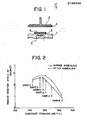
- a (111) oriented monocrystalline GGG substrate 2 is placed on a stainless steel electrode plate 1 also serving as a sample table of an RF sputtering apparatus.
- a target 4 is mounted on an electrode plate 3.
- the target 4 is a sintered ceramics disk of a polycrystalline iron garnet (a composition: Bi 2.0 Y 1.0 Fe 3.8 Al 1.2 O 12 ) with other impurity phases. Since a heater 5 is mounted on the electrode plate 1, the GGG substrate 2 is heated to a predetermined temperature by the heater 5 through the electrode plate 1.
- a predetermined RF voltage is applied between the electrode plates 1 and 3 so as to start glow discharge.
- Ar ions generated by discharge sputter the surface of the target 4, and this sputtering releases atoms such as Bi, Y, Fe, Al and O from the target 4.
- the released atoms are deposited on the GGG substrate 2 which is heated to the predetermined temperature, and a monocrystalline thin film 6 of (Y, Bi) 3 (Fe, Al) 5 O 12 is epitaxially grown on the GGG substrate 2.
- a monocrystalline thin film 6 of (Y, Bi) 3 (Fe, Al) 5 O 12 is epitaxially grown on the GGG substrate 2.
- the thin film 6 is annealed together with the GGG substrate 2 having the film 6 thereon under predetermined conditions so as to remove strain in the thin film 6. X-ray diffractometry of the thin film 6 thus obtained revealed that the film 6 was monocrystalline.
- the monocrystalline thin film 6 manufactured in the first embodiment was observed through an optical microscope, it had an arabesque magnetic domain structure and was proved to be an excellent magnetic thin film having superior characteristics as shown in Figs. 2 to 11..
- the measurement results will sequentially be described hereinbelow.
- a He-Ne laser (wavelength: 6328 A) was used as a light source. Measurement was perforemd by transmitting light through the thin film 6. Measurement of the Curie point shown in Fig. 7 was performed for a sample having a three-layered structure consisting of a GGG substrate 2 having an Al film as a reflecting film on a thin film 6.
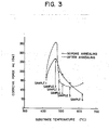
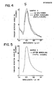
- Figs. 2 and 3 are graphs showing the Faraday rotation angle eF and the coercive force H c of thin films 6 (respective samples are represented by reference numerals 1 to 6, respectively) manufactured at respective substrate temperatures of 420°C, 470°C, 490°C, 510°C, 550°C and 620°C.
- the thin films 6 manufactured on the GGG substrate 2 at 420 to 620°C had Faraday rotation angles e of 1 to 2.75 degree after annealing. Annealing was performed in air at 640°C for 5 hours for samples 1 and 2 and at 740°C for 5 hours for samples 3 to 6.
- the Faraday rotation angles ⁇ F of the thin films 6 manufactured in this embodiment are considerably larger than that of a Bi-substituted rare-earth iron garnet thin film manufactured by the above-mentioned LPE method, i.e., about 0.5 degree.
- the thin films 6 according to the embodiment of the present invention had coercive forces H as high as 140 to 350 Oe, as shown in Fig. 3.
- Fgis. 2 and 3 show the Faraday rotation angle ⁇ F and the coercive force H c of each as-sputtered film 6 together with the data of the Faraday rotation angle ⁇ F and the coercive force H of the film 6 after annealing.
- sample 6 substrate temperature: 620°C
- remaining five samples substrate temperatures: 420 to 550°C had a thickness of 1.5 ⁇ m.
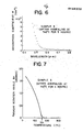
- Fig. 4 shows the light wavelength dependece of the Faraday rotation angle ⁇ F of sample 5 (substrate temperature: 550°C), and Fig. 5 shows the light wavelength dependence of the Faraday rotation angle ⁇ F of sample 3 (substrate temperature: 490°C).
- the Faraday rotation angle e is very large near a wavelength of 0.5 ⁇ m.
- Fig. 4 also shows the measurement result of the as-sputtered film 6 for comparison.
- Fig. 6 shows the wavelength dependence of the absorption coefficient a of the thin film 6 (sample 5). It can be seen from Fig. 6 that the absorption coefficient a of sample 5 is sufficiently small for visible light having a wavelength of 0.55 ⁇ m or more; the thin film 6 is substantially transparent to light in this wavelength range and has an absorption edge near 0.5 ⁇ m.
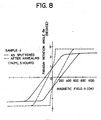
- Fig. 8 shows the hysteresis characteristics of the Faraday rotation angle ⁇ F of sample 4 (substrate temperature: 510°C) as a function of a magnetic field H applied along a direction perpendicular to the film plane.
- the hysteresis characteristics change before and after annealing and the Faraday rotation angle ⁇ F increases after annealing.
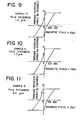
- Figs. 9 to 11 show the hysteresis characteristics of the thin film 6 of sample 5 after annealing, for three different film thicknesses, at the central portion (film thickness: 1.5 ⁇ m) and this peripheral portions (film thicknesses: 1.2 ⁇ m and 0.9 ⁇ m), i.e., 1.5, 1.2 and 0.9 ⁇ m. It can be seen from these figures that the smaller the film thickness, the better the squareness of the loop, and especially when the film thickness is 1 ⁇ m or less, the film exhibits particularly preferable hysteresis characteristics for magneto-optic recording applications.
- the ( F , Bi) 3 (Fe, Al) 5 O 12 monocrystalline thin film 6 manufactured in the first embodiment has a very large Faraday rotation angle ⁇ F , a sufficiently large coercive force H c and a very small absorption coefficient a, thereby providing highly desirable properties as a magneto-optic recording material.
- an amorphous guartz glass is used as the substrate 7, and is heated to 440°C.
- a target 4 similar to that of the first embodiment is used, and the target 4 is sputtered under similar conditions to those in the first embodiment, thereby forming (Y, Bi) 3 (Fe, Al)5012 thin film 6 on the quartz glass substrate 7.
- the sputtering power was 110 W and the sputtering time was 2 hours and a half, the obtained thin film 6 had a thickness of 0.8 ⁇ m.
- the thin film 6 obtained in this manner was annealed in air at 700°C for 3 hours so as to crystallize the thin film 6.
- the film When crystal structure of the thin film 6 manufactured in the second embodiment was examined by X-ray diffractometry, the film was proved to be a polycrystalline film having no preferred orientation. An optical microscope measurement showed that although the film is polycrystalline, it has an arabesque bubble-like magnetic domain structure and was an excellent vertically magnetized film having the following superior characteristics.
- the hysteresis of the Faraday rotation angle c F of the thin film 6 as a function of a magnetic field H applied along a direction perpendicular to the film plane exhibited an excellent squareness.
- the magnetic torque measurement revealed that the film is a vertically magnetized film.
- the film had a large Faraday rotation angle eFof about 1.5 degree and a sufficiently large coercive force H of about 200 Oe.
- the thin film 6 has very desirable properties as a magneto-optic recording material. These may indicate that the film 6 contains the large amount of Bi up to its solid solution limit, applying a large perpendicular magnetic anisotropy.
- a light source for measuring the Faraday rotation angle ⁇ F was a He-Ne laser (wavelength: 6328 A). The measurement was performed by transmitting light through the thin film 6.
- the thin film 6 formed in this manner has relatively small surface roughness adequate to the magneto-optic recording applications.
- a highly Bi-substituted rare-earth, iron garnet thin film which has excellent vertical magnetization characteristics although it is polycrystalline can be formed on a quartz glass substrate having a good productivity.
- the magnetic thin film manufactured in the second ewmbodiment allows direct formation of a reflecting layer thereon, and therefore can be magneto-optic recording medium able to thermomagnetically write using a light with a relatively low power.
- an amorphous thin film 6 of (Y, Bi) 3 (Fe, Al) 5 P 12 having a film thickness of 0.8 ⁇ m is formed on a quartz glass substrate 7 heated to 440°C, as shown in Fig. 12.
- the quartz glass substrate 7 is held at room temperature.
- the sputtering power was 200 W and the sputting time was 30 minutes, the obtained SiO 2 layer 9 had a thickness of 0.5 ⁇ m.
- the thin film 6 manufactured in this manner had no preferred orientation as in the case of the thin film 6 manufactured in the second embodiment.
- the film 6 was observed through an optical microscope, although it was polycrystalline it was found to have an arabesque bubble-like magnetic domain structure and to be an excellent vertically magnetized film having excellent characteristics equivalent to those shown in Fig. 13.
- the protective film constituted by the SiO 2 layer 9 cut-diffusion or atoms sucn as Bi contained in the thin film 6 and surface roughening during annealing can be prevented, and growth of crystal grains of the thin film 6 can be suppressed.
- a polycrystalline vertically magnetized film having excellent characteristics can be formed on a quartz glass substrate 7 having an excellent productivity.
- an SiO 2 layer 9 as a protective film, surface roughness of the thin film 6 resulting from annealing to crystallize the film can be more effectively prevented than in the second embodiment. Since out-diffusion of Bi from the thin film 6 during annealing can be prevented by the SiO 2 layer 9, the annealing temperature can be set to be higher than that in the second embodiment.
Landscapes
- Chemical & Material Sciences (AREA)
- Engineering & Computer Science (AREA)
- Materials Engineering (AREA)
- Physics & Mathematics (AREA)
- Chemical Kinetics & Catalysis (AREA)
- Mechanical Engineering (AREA)
- Metallurgy (AREA)
- Organic Chemistry (AREA)
- Electromagnetism (AREA)
- Power Engineering (AREA)
- General Physics & Mathematics (AREA)
- Thin Magnetic Films (AREA)
Applications Claiming Priority (6)
| Application Number | Priority Date | Filing Date | Title |
|---|---|---|---|
| JP216750/83 | 1983-11-17 | ||
| JP21675083A JPS60107815A (ja) | 1983-11-17 | 1983-11-17 | 磁性薄膜の製造方法 |
| JP6134/84 | 1984-01-17 | ||
| JP613484A JPS60150614A (ja) | 1984-01-17 | 1984-01-17 | 磁性薄膜の製造方法 |
| JP55787/84 | 1984-03-23 | ||
| JP5578784A JPS60200887A (ja) | 1984-03-23 | 1984-03-23 | 磁性薄膜の製造方法 |
Publications (3)
| Publication Number | Publication Date |
|---|---|
| EP0196332A1 true EP0196332A1 (de) | 1986-10-08 |
| EP0196332A4 EP0196332A4 (de) | 1987-09-22 |
| EP0196332B1 EP0196332B1 (de) | 1990-08-01 |
Family
ID=27277022
Family Applications (1)
| Application Number | Title | Priority Date | Filing Date |
|---|---|---|---|
| EP19840904169 Expired EP0196332B1 (de) | 1983-11-17 | 1984-11-15 | Verfahren zur herstellung photothermomagnetischer aufzeichnungsfilme |
Country Status (3)
| Country | Link |
|---|---|
| EP (1) | EP0196332B1 (de) |
| DE (1) | DE3482886D1 (de) |
| WO (1) | WO1985002292A1 (de) |
Cited By (3)
| Publication number | Priority date | Publication date | Assignee | Title |
|---|---|---|---|---|
| FR2655463A1 (fr) * | 1989-12-06 | 1991-06-07 | Commissariat Energie Atomique | Procede de preparation d'une memoire magnetooptique. |
| FR2655462A1 (fr) * | 1989-12-06 | 1991-06-07 | Commissariat Energie Atomique | Procede de preparation d'une memoire magnetooptique. |
| WO2000013178A1 (en) * | 1998-08-28 | 2000-03-09 | Nippon Telegraph And Telephone Corporation | Opto-magnetic recording medium and its manufacturing method, and opto-magnetic information recording/reproducing device |
Families Citing this family (1)
| Publication number | Priority date | Publication date | Assignee | Title |
|---|---|---|---|---|
| DE3424467A1 (de) * | 1984-07-03 | 1986-01-16 | Philips Patentverwaltung Gmbh, 2000 Hamburg | Verfahren zur herstellung wismut-substituierter ferrimagnetischer granatschichten |
Family Cites Families (6)
| Publication number | Priority date | Publication date | Assignee | Title |
|---|---|---|---|---|
| US3607698A (en) * | 1968-10-11 | 1971-09-21 | Ibm | Epitaxial garnet films |
| JPS5020300A (de) * | 1973-06-27 | 1975-03-04 | ||
| JPS5026096A (de) * | 1973-07-06 | 1975-03-18 | ||
| JPS5613710A (en) * | 1979-07-13 | 1981-02-10 | Nec Corp | Material for magnetic element |
| DE3343768A1 (de) * | 1983-12-03 | 1985-06-13 | Philips Patentverwaltung Gmbh, 2000 Hamburg | Verfahren zur herstellung duenner einkristalliner ferrimagnetischer granatschichten durch kathodenzerstaeubung |
| DE3424467A1 (de) * | 1984-07-03 | 1986-01-16 | Philips Patentverwaltung Gmbh, 2000 Hamburg | Verfahren zur herstellung wismut-substituierter ferrimagnetischer granatschichten |
-
1984
- 1984-11-15 WO PCT/JP1984/000547 patent/WO1985002292A1/ja not_active Ceased
- 1984-11-15 EP EP19840904169 patent/EP0196332B1/de not_active Expired
- 1984-11-15 DE DE8484904169T patent/DE3482886D1/de not_active Expired - Lifetime
Cited By (6)
| Publication number | Priority date | Publication date | Assignee | Title |
|---|---|---|---|---|
| FR2655463A1 (fr) * | 1989-12-06 | 1991-06-07 | Commissariat Energie Atomique | Procede de preparation d'une memoire magnetooptique. |
| FR2655462A1 (fr) * | 1989-12-06 | 1991-06-07 | Commissariat Energie Atomique | Procede de preparation d'une memoire magnetooptique. |
| EP0432038A1 (de) * | 1989-12-06 | 1991-06-12 | Commissariat A L'energie Atomique | Verfahren zur Herstellung eines magnetooptischen Speichers |
| US5169504A (en) * | 1989-12-06 | 1992-12-08 | Commissariat A L'energie Atomique | Method for preparing a magneto optic memory |
| WO2000013178A1 (en) * | 1998-08-28 | 2000-03-09 | Nippon Telegraph And Telephone Corporation | Opto-magnetic recording medium and its manufacturing method, and opto-magnetic information recording/reproducing device |
| US6759137B1 (en) | 1998-08-28 | 2004-07-06 | Centre National De La Recherche Scientifique, Inc. | Opto-magnetic recording medium with a garnet ferrite recording layer, and opto-magnetic information recording/reproducing device |
Also Published As
| Publication number | Publication date |
|---|---|
| EP0196332A4 (de) | 1987-09-22 |
| DE3482886D1 (de) | 1990-09-06 |
| EP0196332B1 (de) | 1990-08-01 |
| WO1985002292A1 (fr) | 1985-05-23 |
Similar Documents
| Publication | Publication Date | Title |
|---|---|---|
| Gomi et al. | rf sputtering of highly Bi‐substituted garnet films on glass substrates for magneto‐optic memory | |
| Weller et al. | Magnetic and magneto‐optical properties of cobalt‐platinum alloys with perpendicular magnetic anisotropy | |
| US4608142A (en) | Method of manufacturing magneto-optic recording film | |
| Suzuki | Magnetic and magneto‐optic properties of rapid thermally crystallized garnet films | |
| US4690861A (en) | Magneto optical recording medium | |
| US4624901A (en) | Intermediary layers for epitaxial hexagonal ferrite films | |
| EP0410627A1 (de) | Oxidfilm mit bevorzugter Kristallausrichtung, Verfahren zu dessen Herstellung und magnetooptisches Aufzeichnungsmaterial | |
| JPWO2004067813A1 (ja) | 磁性ガーネット単結晶膜形成用基板、光学素子およびその製造方法 | |
| US5607781A (en) | Oxide film with preferred crystal orientation, method of manufacturing the same, and magneto-optical recording medium | |
| Gomi et al. | RF sputtered films of Bi-substituted garnet for magneto-optical memory | |
| EP0184034A2 (de) | Senkrecht magnetisiertes Aufzeichnungsmedium und Verfahren zu seiner Herstellung | |
| Goml et al. | Sputtered Iron Garner Fills for Magneto-Optical Storage | |
| JPWO2003000963A1 (ja) | 磁性ガーネット単結晶膜形成用基板、光学素子およびその製造方法 | |
| EP0196332A1 (de) | Verfahren zur herstellung photothermomagnetischer aufzeichnungsfilme | |
| JPH0645176A (ja) | 垂直磁気記録媒体の製造方法 | |
| US3539383A (en) | Preparation of manganese bismuth | |
| JPH0354454B2 (de) | ||
| US5041200A (en) | Method of manufacturing crystalline thin-film of rare-earth compounds | |
| Suzuki et al. | Magnetic and magneto-optical properties and crystallization kinetics of rapid-thermally crystallized Bi-substituted garnet films | |
| Park et al. | Chemical composition, microstructure and magnetic characteristics of yttrium iron garnet (YIG, Ce: YIG) thin films grown by rf magnetron sputter techniques | |
| Guzman et al. | Effect of deposition parameters on rf sputtered CoZr and CoZrRe thin films for magnetic recording heads | |
| Tu et al. | Epitaxial growth of EuS films and magnetooptical properties | |
| JPH0558251B2 (de) | ||
| JP2636860B2 (ja) | 光磁気記録用薄膜の製造方法 | |
| JPH0457637B2 (de) |
Legal Events
| Date | Code | Title | Description |
|---|---|---|---|
| PUAI | Public reference made under article 153(3) epc to a published international application that has entered the european phase |
Free format text: ORIGINAL CODE: 0009012 |
|
| 17P | Request for examination filed |
Effective date: 19860516 |
|
| AK | Designated contracting states |
Kind code of ref document: A1 Designated state(s): DE FR GB NL |
|
| A4 | Supplementary search report drawn up and despatched |
Effective date: 19870922 |
|
| 17Q | First examination report despatched |
Effective date: 19890224 |
|
| GRAA | (expected) grant |
Free format text: ORIGINAL CODE: 0009210 |
|
| AK | Designated contracting states |
Kind code of ref document: B1 Designated state(s): DE FR GB NL |
|
| REF | Corresponds to: |
Ref document number: 3482886 Country of ref document: DE Date of ref document: 19900906 |
|
| ET | Fr: translation filed | ||
| PLBE | No opposition filed within time limit |
Free format text: ORIGINAL CODE: 0009261 |
|
| STAA | Information on the status of an ep patent application or granted ep patent |
Free format text: STATUS: NO OPPOSITION FILED WITHIN TIME LIMIT |
|
| 26N | No opposition filed | ||
| PGFP | Annual fee paid to national office [announced via postgrant information from national office to epo] |
Ref country code: GB Payment date: 19911101 Year of fee payment: 8 |
|
| PGFP | Annual fee paid to national office [announced via postgrant information from national office to epo] |
Ref country code: FR Payment date: 19911107 Year of fee payment: 8 |
|
| PGFP | Annual fee paid to national office [announced via postgrant information from national office to epo] |
Ref country code: DE Payment date: 19911129 Year of fee payment: 8 |
|
| PGFP | Annual fee paid to national office [announced via postgrant information from national office to epo] |
Ref country code: NL Payment date: 19911130 Year of fee payment: 8 |
|
| PG25 | Lapsed in a contracting state [announced via postgrant information from national office to epo] |
Ref country code: GB Effective date: 19921115 |
|
| PG25 | Lapsed in a contracting state [announced via postgrant information from national office to epo] |
Ref country code: NL Effective date: 19930601 |
|
| GBPC | Gb: european patent ceased through non-payment of renewal fee |
Effective date: 19921115 |
|
| NLV4 | Nl: lapsed or anulled due to non-payment of the annual fee | ||
| PG25 | Lapsed in a contracting state [announced via postgrant information from national office to epo] |
Ref country code: FR Effective date: 19930730 |
|
| PG25 | Lapsed in a contracting state [announced via postgrant information from national office to epo] |
Ref country code: DE Effective date: 19930803 |
|
| REG | Reference to a national code |
Ref country code: FR Ref legal event code: ST |