EP0196474A2 - Dispositif semi-conducteur constitué de matériau semi-conducteur composé - Google Patents
Dispositif semi-conducteur constitué de matériau semi-conducteur composé Download PDFInfo
- Publication number
- EP0196474A2 EP0196474A2 EP86102757A EP86102757A EP0196474A2 EP 0196474 A2 EP0196474 A2 EP 0196474A2 EP 86102757 A EP86102757 A EP 86102757A EP 86102757 A EP86102757 A EP 86102757A EP 0196474 A2 EP0196474 A2 EP 0196474A2
- Authority
- EP
- European Patent Office
- Prior art keywords
- semiconductor
- isoelectronic
- arrangement according
- layer
- impurity material
- Prior art date
- Legal status (The legal status is an assumption and is not a legal conclusion. Google has not performed a legal analysis and makes no representation as to the accuracy of the status listed.)
- Granted
Links
Images
Classifications
-
- H—ELECTRICITY
- H10—SEMICONDUCTOR DEVICES; ELECTRIC SOLID-STATE DEVICES NOT OTHERWISE PROVIDED FOR
- H10D—INORGANIC ELECTRIC SEMICONDUCTOR DEVICES
- H10D62/00—Semiconductor bodies, or regions thereof, of devices having potential barriers
- H10D62/80—Semiconductor bodies, or regions thereof, of devices having potential barriers characterised by the materials
- H10D62/85—Semiconductor bodies, or regions thereof, of devices having potential barriers characterised by the materials being Group III-V materials, e.g. GaAs
- H10D62/854—Semiconductor bodies, or regions thereof, of devices having potential barriers characterised by the materials being Group III-V materials, e.g. GaAs further characterised by the dopants
Definitions
- Compound semiconductor material is often used in the manufacture of electronic components.
- the most common compound semiconductor materials consist of substances from III. and V. group of the periodic system, in particular from galium arsenide or indium phosphide. Multiple connections, for example made of GaA1As, GaInAs or GaInAsP, are also often used.
- semiconductor LASER optoelectronic components
- semiconductor LASER components with Schottky transitions and integrated semiconductor circuits are manufactured.
- the manufacture of the components mentioned is based on a basic body which can be melted in various ways, for example by zone melting, using the horizontal Bridgman method or can be produced by the LEC process (Liquid encapsulated Czochralski).
- One or more semiconductor layers are applied to this base body, preferably by epitaxial deposition.
- the quality of the epitaxial layers by Fl u s - sigphasenepitaxie or can be separated off by vapor phase epitaxy, is the dislocation density in Semiconductor base body crucial. For each further growing epitaxial layer, it is essential how large the dislocation density is in the underlying epitaxial layers. Dislocation densities between 10 4 -10 5 / cm 2 are given as relatively low in the literature. However, the values for the dislocation density are much too large for the production of high quality components. For example, for the production of field effect transistors, certain structures are built into the base body with the dislocation densities mentioned by implanting impurities. The electrical characteristic values of these field effect transistors are considerably deteriorated by the high dislocation density in the base body.
- the dislocations that continue in the epitaxial layers also cause serious disturbances when building multilayer structures with heterojunctions.
- layers are deposited on a base body which do not have the exact same grid spacing from one another and from the semiconductor base body.
- the base body often consists of a double compound semiconductor such as gallium arsenide or indium phosphide, on which layers of ternary or quaternary material such as GaAlAs or GalnAsP are deposited. Since the lattice spacing of the materials of the different layers does not match exactly, but a single-crystal growth is required, it is easy to understand that a high dislocation density in the base body or in the base layer provided for the deposition has a very disruptive effect.
- the invention is based on the object of specifying a semiconductor arrangement made of compound semiconductor material, the semiconductor body in parts or in the case of certain materials in its entirety having a dislocation density which is substantially reduced compared to the known arrangements.
- This object is achieved according to the invention in that the semiconductor body contains isoelectronic impurity material from one element in parts, the coiral atomic radius of which is greater than that of the element of the compound semiconductor to which the impurity material is isoelectronic.
- the semiconductor body consists of a phosphide compound and, in its entirety or in part, contains isoelectronic impurity material from an element whose covalent atomic radius is greater than that of the element of the compound semiconductor to which the impurity material is isoelectronic.
- tension centers By installing tension centers according to the invention, fixation and thus termination of the further growth of dislocations in the epitaxial layers is achieved during their manufacture. These stress centers should not cause any additional, undesirable doping of the semiconductor body, which is due to the use of isoelectronic interference job material is reached. As a result, the incorporation of interfering atoms that are not III. or V. group belong to the periodic table.
- the semiconductor arrangements according to the invention preferably consist of III / V compound semiconductor material.
- the connecting material is, for example, indium phosphide, arsenic, antimony or bismuth is suitable as the isoelectronic impurity material.
- Aluminum and gallium are isoelectronic with indium, but both atoms have a smaller covalent radius than indium and are therefore not suitable for compensation of the dislocations.
- arsenic, antimony and bismuth which are isoelectronic to phosphorus, are provided with a larger covalent atomic radius, so that an effective compensation of the dislocations can be achieved with these elements.
- the III. Group of the periodic system in particular of indium, achieves a considerable reduction in the dislocation density, which is in turn due to the fact that indium has a larger covalent atomic radius than that of the indium isoelectronic gallium.
- the semiconductor arrangement according to the invention is preferably of multilayer design, it being sufficient to introduce the isoelectronic impurity material only into a first layer, which thus has a very low dislocation density of approximately 10 3 cm -2 and smaller.
- the epitaxial layers applied to this modified base body then likewise grow up with a very low dislocation density, so that the components to be produced have significantly improved electrical properties.
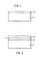
- a base body 1 which consists of indium phosphide and was produced by the known LEC process.
- This semiconductor body is uniformly doped with arsenic during the manufacturing process, in a concentration that is preferably greater than 5 ⁇ 10 18 atoms / cm 3 .
- the dislocation density of this base body is 1 0 3 cm -2 .
- One or more epitaxial layers 2 with a low dislocation density can then be deposited on this base body without having to add isoelectronic impurities during the layer deposition.
- the base body can also consist of gallium phosphide or aluminum phosphide.
- the arrangement according to FIG. 2 is based on a base body 1, which consists, for example, of indium phosphide and contains no isoelectronic impurities.
- the dislocation density in this base body is 10 4 - 10 5 / cm 2 .
- the epitaxial layer 2 also consists of indium phosphide, arsenic with an impurity concentration greater than 5 ⁇ 10 18 atoms / cm, antimony or bismuth is again suitable as the isoelectronic impurity material.
- the epitaxial layer can also consist of ternary or quaternary material such as GaInAs or GaInAsP. In this case, antimony or bismuth is suitable as an isoelectronic impurity material.
- the isoelectronic impurities cause a slight change in the lattice constant, which is less than 10 -4 . Normally, this slight change in the lattice constant does not interfere with the further opening grow the epitaxial layers. However, if the lattice constant of the base body 1 deviates from that of the epitaxial layer 2 to be grown in the case of heterojunctions, it is advisable to add the isoelectronic impurity material to the material for the epitaxially grown semiconductor layer in such a way that the concentration increases with the growth of the layer, that is to say in the direction of growth . This can be done by continuously increasing the concentration of isoelectronic impurities in the melt in liquid phase epitaxy.
- layer 2 is produced by liquid phase epitaxy with a maximum of impurities
- the proportion of isoelectronic impurities in the melt is initially continuous during the growth process increase. After reaching the maximum, the concentration of the isoelectronic impurities will be reduced, for example, by continuously increasing the proportion of the other constituents in the melt.
- isoelectronic impurities both in the base body and in one or more grown epitaxial layers.
- a corresponding procedure can be used for the layer production by the gas phase epitaxy process, in which case the isoelectronic doping can also be carried out by supplying corresponding gaseous components.
- the material proportion of the isoelectronic substance is preferably less than 0.5% of the element to which the substance is isoelectronic. Experimental experiments have shown that values between 0.1 and 0.3% are completely sufficient.
- the semiconductor arrangement according to the invention and the method for its production are particularly suitable for the production of optoelectronic components, laser arrangements, memory components, integrated circuits and components with Schottky contacts.
Landscapes
- Recrystallisation Techniques (AREA)
- Liquid Deposition Of Substances Of Which Semiconductor Devices Are Composed (AREA)
- Chemical Vapour Deposition (AREA)
Applications Claiming Priority (2)
| Application Number | Priority Date | Filing Date | Title |
|---|---|---|---|
| DE19853508024 DE3508024A1 (de) | 1985-03-07 | 1985-03-07 | Halbleiteranordnung aus verbindungshalbleitermaterial |
| DE3508024 | 1985-03-07 |
Publications (3)
| Publication Number | Publication Date |
|---|---|
| EP0196474A2 true EP0196474A2 (fr) | 1986-10-08 |
| EP0196474A3 EP0196474A3 (fr) | 1989-04-05 |
| EP0196474B1 EP0196474B1 (fr) | 1997-08-06 |
Family
ID=6264417
Family Applications (1)
| Application Number | Title | Priority Date | Filing Date |
|---|---|---|---|
| EP86102757A Expired - Lifetime EP0196474B1 (fr) | 1985-03-07 | 1986-03-03 | Dispositif semi-conducteur constitué de matériau semi-conducteur composé |
Country Status (4)
| Country | Link |
|---|---|
| US (1) | US5422731A (fr) |
| EP (1) | EP0196474B1 (fr) |
| JP (1) | JP2663965B2 (fr) |
| DE (1) | DE3508024A1 (fr) |
Cited By (1)
| Publication number | Priority date | Publication date | Assignee | Title |
|---|---|---|---|---|
| DE102013002400A1 (de) | 2013-02-13 | 2014-08-14 | Otto-Von Guericke-Universität Magdeburg Technologie-Transfer-Zentrum | Vorrichtung zur Bilderfassung in Bildgebungssystemen sowie Verfahren hierfür |
Families Citing this family (4)
| Publication number | Priority date | Publication date | Assignee | Title |
|---|---|---|---|---|
| US8507361B2 (en) * | 2000-11-27 | 2013-08-13 | Soitec | Fabrication of substrates with a useful layer of monocrystalline semiconductor material |
| US6815736B2 (en) * | 2001-02-09 | 2004-11-09 | Midwest Research Institute | Isoelectronic co-doping |
| GB0911134D0 (en) * | 2009-06-26 | 2009-08-12 | Univ Surrey | Optoelectronic devices |
| WO2011112612A1 (fr) | 2010-03-08 | 2011-09-15 | Alliance For Sustainable Energy, Llc | Co-dopage au bore et au bismuth d'arséniure de gallium et d'autres composés pour dispositifs transistors bipolaires photoniques et à hétérojonction |
Family Cites Families (8)
| Publication number | Priority date | Publication date | Assignee | Title |
|---|---|---|---|---|
| SE338761B (fr) * | 1967-10-20 | 1971-09-20 | Philips Nv | |
| US3982261A (en) * | 1972-09-22 | 1976-09-21 | Varian Associates | Epitaxial indium-gallium-arsenide phosphide layer on lattice-matched indium-phosphide substrate and devices |
| US3958143A (en) * | 1973-01-15 | 1976-05-18 | Varian Associates | Long-wavelength photoemission cathode |
| US4237471A (en) * | 1979-06-22 | 1980-12-02 | Hamamatsu Corporation | Method of producing a semiconductor photodiode of indium antimonide and device thereof |
| US4450463A (en) * | 1981-06-29 | 1984-05-22 | Rockwell International Corporation | Multiple-quantum-layer photodetector |
| JPS60105218A (ja) * | 1983-11-11 | 1985-06-10 | Nippon Telegr & Teleph Corp <Ntt> | 3−5族化合物単結晶半導体基板 |
| JPS60176997A (ja) * | 1984-02-23 | 1985-09-11 | Sumitomo Electric Ind Ltd | 低転位密度の3−5化合物半導体単結晶 |
| JPS6185814A (ja) * | 1984-10-03 | 1986-05-01 | Nec Corp | 化合物半導体結晶ウエ−ハ |
-
1985
- 1985-03-07 DE DE19853508024 patent/DE3508024A1/de active Granted
-
1986
- 1986-03-03 EP EP86102757A patent/EP0196474B1/fr not_active Expired - Lifetime
- 1986-03-06 JP JP61047480A patent/JP2663965B2/ja not_active Expired - Fee Related
-
1990
- 1990-09-12 US US07/581,413 patent/US5422731A/en not_active Expired - Fee Related
Cited By (1)
| Publication number | Priority date | Publication date | Assignee | Title |
|---|---|---|---|---|
| DE102013002400A1 (de) | 2013-02-13 | 2014-08-14 | Otto-Von Guericke-Universität Magdeburg Technologie-Transfer-Zentrum | Vorrichtung zur Bilderfassung in Bildgebungssystemen sowie Verfahren hierfür |
Also Published As
| Publication number | Publication date |
|---|---|
| DE3508024C2 (fr) | 1991-05-16 |
| US5422731A (en) | 1995-06-06 |
| JPS61206216A (ja) | 1986-09-12 |
| JP2663965B2 (ja) | 1997-10-15 |
| EP0196474B1 (fr) | 1997-08-06 |
| DE3508024A1 (de) | 1986-09-11 |
| EP0196474A3 (fr) | 1989-04-05 |
Similar Documents
| Publication | Publication Date | Title |
|---|---|---|
| DE2416550C2 (de) | Verfahren zum Herstellen eines Halbleiterbauelements mit versetzungsfreiem Übergitterstrukturkristall | |
| DE69327483T2 (de) | Diode und Verfahren zur Herstellung | |
| DE69431333T2 (de) | GaN-Einkristall | |
| DE69903783T2 (de) | Nitrid-Halbleitervorrichtung und ihr Herstellungsverfahren | |
| DE2830081A1 (de) | Verfahren zum herstellen eines halbleitermateriales der gruppen iii/v des periodischen systems | |
| DE2231926A1 (de) | Verfahren zur herstellung von halbleitermaterial und zur herstellung von halbleitereinrichtungen | |
| DE69525700T2 (de) | Verfahren zur Herstellung einer lichtemittierenden Halbleitervorrichtung | |
| DE19615179B4 (de) | Verfahren zur Herstellung lichtemittierender Halbleiterbauelemente mit verbesserter Stabilität | |
| DE2005271C3 (de) | Epitaxialverfahren zum Aufwachsen von Halbleitermaterial auf einem dotierten Halbleitersubstrat | |
| DE3012119C2 (de) | Verfahren zum Herstellen eines Halbleiterbauelements | |
| DE19806536A1 (de) | Grünes Licht emittierendes Galliumphosphid-Bauteil | |
| DE2212489C3 (de) | Verfahren zur Herstellung eines Feldeffekttransistors | |
| DE2734203A1 (de) | Hetero-uebergangslaser | |
| EP0196474B1 (fr) | Dispositif semi-conducteur constitué de matériau semi-conducteur composé | |
| DE3887790T2 (de) | Lichtemittierende Halbleitervorrichtung. | |
| DE3324220C2 (de) | Gallium-Phosphid-Leuchtdiode | |
| DE2843983C2 (de) | Verfahren zum Herstellen einer Grünlicht emittierenden GaP-Lumineszenzdiode | |
| DE2544286C3 (de) | Verfahren zum epitaktischen Abscheiden einer III-V-Halbleiterkristallschicht auf einem Substrat | |
| DE2154386B2 (de) | Verfahren zum Herstellen einer epitaktischen Halbleiterschicht auf einem Halbleitersubstrat durch Abscheiden aus einem Reaktionsgas/Trägergas-Gemisch | |
| DE69207069T2 (de) | Lichtemittierende Halbleitervorrichtung | |
| DE69514304T2 (de) | Lichtemittierende Vorrichtung | |
| DE69313573T2 (de) | Verfahren zur Herstellung eines GaP lichtemittierenden Elementes | |
| DE4319233B4 (de) | Epitaxialwafer aus Galliumaresenidphosphid | |
| DE2420741C2 (de) | Herstellungsverfahren für eine Leuchtdiode | |
| WO2004021457A2 (fr) | Procede de fabrication d'une puce a semiconducteurs emettant un rayonnement electromagnetique et puce a semiconducteurs emettant un rayonnement electromagnetique |
Legal Events
| Date | Code | Title | Description |
|---|---|---|---|
| PUAI | Public reference made under article 153(3) epc to a published international application that has entered the european phase |
Free format text: ORIGINAL CODE: 0009012 |
|
| AK | Designated contracting states |
Kind code of ref document: A2 Designated state(s): FR GB IT NL |
|
| PUAL | Search report despatched |
Free format text: ORIGINAL CODE: 0009013 |
|
| RHK1 | Main classification (correction) |
Ipc: H01L 29/207 |
|
| AK | Designated contracting states |
Kind code of ref document: A3 Designated state(s): FR GB IT NL |
|
| 17P | Request for examination filed |
Effective date: 19890912 |
|
| 17Q | First examination report despatched |
Effective date: 19910124 |
|
| RAP1 | Party data changed (applicant data changed or rights of an application transferred) |
Owner name: TEMIC TELEFUNKEN MICROELECTRONIC GMBH |
|
| APAB | Appeal dossier modified |
Free format text: ORIGINAL CODE: EPIDOS NOAPE |
|
| GRAG | Despatch of communication of intention to grant |
Free format text: ORIGINAL CODE: EPIDOS AGRA |
|
| GRAH | Despatch of communication of intention to grant a patent |
Free format text: ORIGINAL CODE: EPIDOS IGRA |
|
| GRAH | Despatch of communication of intention to grant a patent |
Free format text: ORIGINAL CODE: EPIDOS IGRA |
|
| GRAA | (expected) grant |
Free format text: ORIGINAL CODE: 0009210 |
|
| AK | Designated contracting states |
Kind code of ref document: B1 Designated state(s): FR GB IT NL |
|
| GBT | Gb: translation of ep patent filed (gb section 77(6)(a)/1977) |
Effective date: 19970808 |
|
| ET | Fr: translation filed | ||
| PLBE | No opposition filed within time limit |
Free format text: ORIGINAL CODE: 0009261 |
|
| STAA | Information on the status of an ep patent application or granted ep patent |
Free format text: STATUS: NO OPPOSITION FILED WITHIN TIME LIMIT |
|
| 26N | No opposition filed | ||
| NLS | Nl: assignments of ep-patents |
Owner name: VISHAY SEMICONDUCTOR GMBH |
|
| REG | Reference to a national code |
Ref country code: GB Ref legal event code: 732E |
|
| REG | Reference to a national code |
Ref country code: FR Ref legal event code: TP |
|
| REG | Reference to a national code |
Ref country code: GB Ref legal event code: IF02 |
|
| PGFP | Annual fee paid to national office [announced via postgrant information from national office to epo] |
Ref country code: GB Payment date: 20030226 Year of fee payment: 18 |
|
| PGFP | Annual fee paid to national office [announced via postgrant information from national office to epo] |
Ref country code: NL Payment date: 20030228 Year of fee payment: 18 |
|
| PGFP | Annual fee paid to national office [announced via postgrant information from national office to epo] |
Ref country code: FR Payment date: 20030314 Year of fee payment: 18 |
|
| PG25 | Lapsed in a contracting state [announced via postgrant information from national office to epo] |
Ref country code: GB Free format text: LAPSE BECAUSE OF NON-PAYMENT OF DUE FEES Effective date: 20040303 |
|
| PG25 | Lapsed in a contracting state [announced via postgrant information from national office to epo] |
Ref country code: NL Free format text: LAPSE BECAUSE OF NON-PAYMENT OF DUE FEES Effective date: 20041001 |
|
| GBPC | Gb: european patent ceased through non-payment of renewal fee | ||
| PG25 | Lapsed in a contracting state [announced via postgrant information from national office to epo] |
Ref country code: FR Free format text: LAPSE BECAUSE OF NON-PAYMENT OF DUE FEES Effective date: 20041130 |
|
| NLV4 | Nl: lapsed or anulled due to non-payment of the annual fee |
Effective date: 20041001 |
|
| REG | Reference to a national code |
Ref country code: FR Ref legal event code: ST |
|
| PG25 | Lapsed in a contracting state [announced via postgrant information from national office to epo] |
Ref country code: IT Free format text: LAPSE BECAUSE OF NON-PAYMENT OF DUE FEES;WARNING: LAPSES OF ITALIAN PATENTS WITH EFFECTIVE DATE BEFORE 2007 MAY HAVE OCCURRED AT ANY TIME BEFORE 2007. THE CORRECT EFFECTIVE DATE MAY BE DIFFERENT FROM THE ONE RECORDED. Effective date: 20050303 |
|
| APAH | Appeal reference modified |
Free format text: ORIGINAL CODE: EPIDOSCREFNO |