EP0196883A2 - Aktive Filterschaltungen - Google Patents
Aktive Filterschaltungen Download PDFInfo
- Publication number
- EP0196883A2 EP0196883A2 EP86302276A EP86302276A EP0196883A2 EP 0196883 A2 EP0196883 A2 EP 0196883A2 EP 86302276 A EP86302276 A EP 86302276A EP 86302276 A EP86302276 A EP 86302276A EP 0196883 A2 EP0196883 A2 EP 0196883A2
- Authority
- EP
- European Patent Office
- Prior art keywords
- transistor
- circuit
- active filter
- filter circuit
- collector
- Prior art date
- Legal status (The legal status is an assumption and is not a legal conclusion. Google has not performed a legal analysis and makes no representation as to the accuracy of the status listed.)
- Granted
Links
Images

Classifications
-
- H—ELECTRICITY
- H03—ELECTRONIC CIRCUITRY
- H03H—IMPEDANCE NETWORKS, e.g. RESONANT CIRCUITS; RESONATORS
- H03H11/00—Networks using active elements
- H03H11/02—Multiple-port networks
- H03H11/04—Frequency selective two-port networks
-
- H—ELECTRICITY
- H03—ELECTRONIC CIRCUITRY
- H03H—IMPEDANCE NETWORKS, e.g. RESONANT CIRCUITS; RESONATORS
- H03H11/00—Networks using active elements
- H03H11/02—Multiple-port networks
- H03H11/04—Frequency selective two-port networks
- H03H11/12—Frequency selective two-port networks using amplifiers with feedback
- H03H11/1213—Frequency selective two-port networks using amplifiers with feedback using transistor amplifiers
Definitions
- This invention relates to active filter circuits.
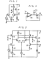
- Figure 1 shows an example of a previously proposed low pass filter.
- one side of an input signal source 1 is connected to the base of an npn transistor 2 while the other side of the input signal source 1 is grounded.
- the collector of the transistor 2 is connected to a voltage source terminal 3 to which a positive dc voltage is applied.
- the emitter of the transistor 2 is connected to the emitter of an npn transistor 4 and the junction or connection point between the emitters of the transistors 2 and 4 is grounded via a constant current circuit 5 through which a predetermined current I flows.
- the collector of the transistor 4 is connected to the voltage source terminal 3 via a constant current source circuit 6. Also, the collector of the transistor 4 is grounded via a capacitor 7 having a capacitance C which forms a load.
- the collector of the transistor 4 is further connected to the base of an npn transistor 8 which forms an emitter-follower circuit of a feedback loop.
- the collector of the transistor 8 is connected to the voltage source terminal 3 and the emitter of the transistor 8 is grounded via a constant current circuit 9.
- the emitter of the transistor 8 is further connected to the base of the transistor 4 and an output terminal 10 is led out from the emitter of the transistor 8.
- the Gm feedback type primary filter circuit shown in Figure 3 will be described briefly. If the level of an input signal supplied to an input terminal la is taken as L, the amplification factor of a differential amplifier circuit 2a is taken as (1/r), the dc voltage supplied to a voltage source terminal 3a is taken as H, the capacitance of a capacitor 7 is taken as C and an output level generated at an output terminal 10 is taken as X, the following relationships are established: and
- Figure 2 shows another example of a previously proposed primary low pass filter.
- the primary low pass filter of Figure 2 employs a so-called Gilbert circuit.
- one side of an input signal source 1 is connected to the base of an npn transistor 11 while the other end of the source 1 is grounded.
- the emitter of the transistor 11 is grounded via a series circuit formed of a resistor 12 having a resistance R and a constant current circuit 13 having a current I.
- the collector of the transistor 11 is connected to the emitter of an npn transistor 14, the collector of which is connected to a voltage source terminal 3.
- the base of the transistor 14 is grounded via a battery 15.
- the collector of the transistor 11 is connected to the base of an npn transistor 16, the collector of which is connected to the voltage source terminal 3 via a constant current circuit 17.
- the emitter of the transistor 16 is connected to the emitter of an npn transistor 18, and the junction between the emitters of the transistors 16 and 18 is grounded via a constant current circuit 19 having a constant current L
- the collector of the transistor 18 is connected to the voltage source terminal 3.
- the base of the transistor 18 is connected to the collector of an npn transistor 20, the emitter of which is connected through a resistor 21 having a resistance R to the junction between the resistor 12 and the constant current circuit 13.
- the collector of the transistor 20 is connected to the emitter of an npn transistor 22, the collector of which is connected to the voltage source terminal 3.
- the base of the transistor 22 is connected to the base of the transistor 14.
- the collector of the transistor 16 is grounded via a capacitor 7 having a capacitance C which forms a load.
- the collector of the transistor 16 is connected to the base of an npn transistor 23 which forms an emitter-follower circuit of a feedback loop.
- the collector of the transistor 23 is connected to the voltage source terminal 3 and the emitter of the transistor 23 is grounded via a series circuit formed of a resistor 24 and a constant current circuit 25.
- the junction between the resistor 24 and the constant current circuit 25 is connected to the base of the transistor 20 and an output terminal 10 is led out from the junction between the resistor 24 and the constant current circuit 25.
- the active filter circuit shown in Figure 2 forms a mutual conductance (Gm) feedback type primary filter circuit as shown in Figure 3 and its filter characteristic H(LV) is represented by
- an active filter circuit comprising:
- one end of the input signal source 1 is connected to the base of an npn transistor 26 while the other end of the signal source 1 is grounded.
- the collector of the transistor 26 is connected to the voltage source terminal 3, while the emitter of the transistor 26 is connected through a resistor 27 having a resistance value R to a junction between the base and collector of an npn transistor 28 (which forms a diode) and is also connected to the base of an npn transistor 29.
- the transistors 28 and 29 constitute a differential amplifier circuit.
- the emitter of the transistor 28 is grounded via a constant current circuit 34 having a constant current I I'
- the collector of the transistor 29 is connected to the voltage source terminal 3 and the emitter of the transistor 29 is connected to the emitter of an npn transistor 30 which forms, together with the transistor 29, a differential amplifier circuit.
- the junction between the emitters of the transistors 29 and 30 is grounded via a constant current circuit 33 having a constant current I2.
- the collector of the transistor 30 is connected to the voltage source terminal 3 via a constant current source 35, while the collector of the transistor 30 is grounded via the capacitor 7 which forms a reactance circuit serving as a load.
- the output terminal 10 is led out from the collector of the transistor 30, which collector is connected to the base of an npn transistor 31.
- the collector of the transistor 31 is connected to the voltage source terminal 3 and the emitter of this transistor 31 is connected through a resistor 32 having a resistance value R 1 to a junction between the base and collector of an npn transistor 36 (which forms a diode) and to the base of the transistor 30.
- the emitter of the transistor 36 is connected to the emitter of the transistor 28.
- the active filter circuit shown in Figure 4 also forms a Gm feedback type primary filter circuit having the construction shown in principle in Figure 3.
- I 1 1 2' its filter characteristic H ( ⁇ ) is given as
- the active filter circuit of Figure 4 is a low pass filter circuit in which the condition is satisfied.
- the dynamic range of the active filter circuit according to the embodiment of Figure 4 is determined by I 2 (2R 1 + 4re) so that this dynamic range can be widened similarly to the previously proposed example of Figure 2.
- the emitter-follower circuit since the emitter-follower circuit is not required in the feedback circuit, it is possible to reduce the number of circuit elements. For example, it is possible to reduce the number of circuit elements by 20% as compared with the example of Figure 2. Therefore, this embodiment of the invention is particularly advantageous when used in an LSI circuit which employs a large number of active filter circuit elements.
- the phase characteristic of the active filter circuit is never affected so that the active filter circuit of this embodiment has an excellent phase characteristic in the high frequency band, thus presenting a satisfactory frequency characteristic.
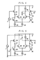
- Figure 5 shows another active filter circuit embodying the present invention which operates as a high pass filter circuit.
- parts corresponding to like parts of Figure 4 are designated by the same references and will not be described again.
- one end of the input signal source 1 is connected through the capacitor 7 forming a reactance circuit to the collector of the transistor 30 and the other end of the signal source 1 is grounded.
- the base of the transistor 26 is grounded via a battery 37 which generates a predetermined dc voltage.
- the circuit otherwise is formed in the same way as in Figure 4.
- the active filter circuit shown in Figure 5 forms a Gm feedback type primary filter circuit as shown in Figure 3 and also forms a high pass filter circuit. It will easily be understood that the embodiment shown in Figure 5 can achieve the same action and effect as that of Figure 4.
- Figure 6 shows another active filter circuit embodying the present invention which operates as a secondary low pass filter.
- parts corresponding to like parts of Figure 4 are designated by the same references suffixed with a and b. From Figure 6, it will easily be understood that the active filter circuit according to this embodiment can achieve the same action and effect as that of Figure 4.
- embodiments of the present invention make it possible to realise an active filter circuit which does not depend on the internal resistance of a semiconductor integrated circuit. Accordingly, when the active filter circuit is formed into a semiconductor integrated circuit, it is possible to obtain an active filter circuit which has an excellent temperature characteristic and whose filter characteristic can be prevented from being scattered.
Landscapes
- Networks Using Active Elements (AREA)
- Filtering Of Dispersed Particles In Gases (AREA)
Priority Applications (1)
| Application Number | Priority Date | Filing Date | Title |
|---|---|---|---|
| AT86302276T ATE77021T1 (de) | 1985-03-29 | 1986-03-26 | Aktive filterschaltungen. |
Applications Claiming Priority (2)
| Application Number | Priority Date | Filing Date | Title |
|---|---|---|---|
| JP65872/85 | 1985-03-29 | ||
| JP60065872A JPH0738557B2 (ja) | 1985-03-29 | 1985-03-29 | アクテイブフイルタ−回路 |
Publications (3)
| Publication Number | Publication Date |
|---|---|
| EP0196883A2 true EP0196883A2 (de) | 1986-10-08 |
| EP0196883A3 EP0196883A3 (en) | 1988-05-18 |
| EP0196883B1 EP0196883B1 (de) | 1992-06-03 |
Family
ID=13299501
Family Applications (1)
| Application Number | Title | Priority Date | Filing Date |
|---|---|---|---|
| EP86302276A Expired - Lifetime EP0196883B1 (de) | 1985-03-29 | 1986-03-26 | Aktive Filterschaltungen |
Country Status (7)
| Country | Link |
|---|---|
| US (1) | US4689580A (de) |
| EP (1) | EP0196883B1 (de) |
| JP (1) | JPH0738557B2 (de) |
| KR (1) | KR940009398B1 (de) |
| AT (1) | ATE77021T1 (de) |
| CA (1) | CA1248186A (de) |
| DE (1) | DE3685506T2 (de) |
Cited By (1)
| Publication number | Priority date | Publication date | Assignee | Title |
|---|---|---|---|---|
| EP0375790A1 (de) * | 1988-10-13 | 1990-07-04 | Siemens Aktiengesellschaft | Integrierbare Filterschaltung |
Families Citing this family (6)
| Publication number | Priority date | Publication date | Assignee | Title |
|---|---|---|---|---|
| EP0392062B1 (de) * | 1989-04-14 | 1994-06-22 | Siemens Aktiengesellschaft | Integrierbare Verstärkerschaltung |
| NL8901837A (nl) * | 1989-07-17 | 1991-02-18 | Philips Nv | Filterschakeling met een versterker en een kondensator. |
| NL9001966A (nl) * | 1990-09-06 | 1992-04-01 | Philips Nv | Versterkerschakeling. |
| JP3333239B2 (ja) * | 1991-12-05 | 2002-10-15 | 株式会社東芝 | 可変利得回路 |
| JP3411988B2 (ja) * | 1992-09-21 | 2003-06-03 | 株式会社東芝 | 可変電圧電流変換回路 |
| JP3507530B2 (ja) * | 1993-09-16 | 2004-03-15 | 株式会社東芝 | 対数変換回路 |
Family Cites Families (3)
| Publication number | Priority date | Publication date | Assignee | Title |
|---|---|---|---|---|
| JPS55611A (en) * | 1978-06-09 | 1980-01-07 | Toshiba Corp | Constant current circuit |
| JPS5545224A (en) * | 1978-09-26 | 1980-03-29 | Sony Corp | Filter circuit |
| CA1134463A (en) * | 1978-10-13 | 1982-10-26 | Kyoichi Murakami | Circuit for converting single-ended input signals to a pair of differential output signals |
-
1985
- 1985-03-29 JP JP60065872A patent/JPH0738557B2/ja not_active Expired - Lifetime
-
1986
- 1986-03-24 KR KR1019860002174A patent/KR940009398B1/ko not_active Expired - Lifetime
- 1986-03-26 AT AT86302276T patent/ATE77021T1/de not_active IP Right Cessation
- 1986-03-26 CA CA000505128A patent/CA1248186A/en not_active Expired
- 1986-03-26 EP EP86302276A patent/EP0196883B1/de not_active Expired - Lifetime
- 1986-03-26 DE DE8686302276T patent/DE3685506T2/de not_active Expired - Lifetime
- 1986-03-27 US US06/844,983 patent/US4689580A/en not_active Expired - Lifetime
Cited By (1)
| Publication number | Priority date | Publication date | Assignee | Title |
|---|---|---|---|---|
| EP0375790A1 (de) * | 1988-10-13 | 1990-07-04 | Siemens Aktiengesellschaft | Integrierbare Filterschaltung |
Also Published As
| Publication number | Publication date |
|---|---|
| DE3685506T2 (de) | 1993-01-28 |
| EP0196883B1 (de) | 1992-06-03 |
| EP0196883A3 (en) | 1988-05-18 |
| KR940009398B1 (ko) | 1994-10-07 |
| CA1248186A (en) | 1989-01-03 |
| ATE77021T1 (de) | 1992-06-15 |
| KR860007780A (ko) | 1986-10-17 |
| JPS61224715A (ja) | 1986-10-06 |
| JPH0738557B2 (ja) | 1995-04-26 |
| US4689580A (en) | 1987-08-25 |
| DE3685506D1 (de) | 1992-07-09 |
Similar Documents
| Publication | Publication Date | Title |
|---|---|---|
| KR950010479B1 (ko) | 액티브필터 | |
| JPS6155806B2 (de) | ||
| US4109214A (en) | Unbalanced-to-balanced signal converter circuit | |
| EP0196883A2 (de) | Aktive Filterschaltungen | |
| KR940001817B1 (ko) | 노이즈 감소회로에 사용되는 액티브 필터용 고역 가중치 회로 | |
| US4352057A (en) | Constant current source | |
| JPH0770935B2 (ja) | 差動電流増幅回路 | |
| US4017749A (en) | Transistor circuit including source voltage ripple removal | |
| US5155429A (en) | Threshold voltage generating circuit | |
| JPH0690656B2 (ja) | 基準電圧の形成回路 | |
| EP0690562A1 (de) | Transkonduktanzschaltung mit hohem linearen Differenzeingang und seine Verwendung in aktivem Filter | |
| US5475327A (en) | Variable impedance circuit | |
| JP2628663B2 (ja) | 電流ミラー回路 | |
| JPS6228087Y2 (de) | ||
| JPH0129852Y2 (de) | ||
| JPH04369916A (ja) | ノイズ減衰回路に使われるアクティブ高域加重値回路 | |
| JPS607213A (ja) | 差動段 | |
| US5015967A (en) | Integratable amplifier circuit | |
| JPH0642250Y2 (ja) | 負出力電圧安定化電源回路 | |
| JPH0451085B2 (de) | ||
| JPS5939114A (ja) | 自動利得制御信号検出装置 | |
| JP3148469B2 (ja) | フィルタ回路 | |
| RU2076351C1 (ru) | Источник образцовых напряжений | |
| JPH0454404B2 (de) | ||
| JPS6313363B2 (de) |
Legal Events
| Date | Code | Title | Description |
|---|---|---|---|
| PUAI | Public reference made under article 153(3) epc to a published international application that has entered the european phase |
Free format text: ORIGINAL CODE: 0009012 |
|
| AK | Designated contracting states |
Kind code of ref document: A2 Designated state(s): AT DE FR GB NL |
|
| PUAL | Search report despatched |
Free format text: ORIGINAL CODE: 0009013 |
|
| AK | Designated contracting states |
Kind code of ref document: A3 Designated state(s): AT DE FR GB NL |
|
| 17P | Request for examination filed |
Effective date: 19881021 |
|
| 17Q | First examination report despatched |
Effective date: 19901025 |
|
| GRAA | (expected) grant |
Free format text: ORIGINAL CODE: 0009210 |
|
| AK | Designated contracting states |
Kind code of ref document: B1 Designated state(s): AT DE FR GB NL |
|
| REF | Corresponds to: |
Ref document number: 77021 Country of ref document: AT Date of ref document: 19920615 Kind code of ref document: T |
|
| REF | Corresponds to: |
Ref document number: 3685506 Country of ref document: DE Date of ref document: 19920709 |
|
| ET | Fr: translation filed | ||
| PLBE | No opposition filed within time limit |
Free format text: ORIGINAL CODE: 0009261 |
|
| STAA | Information on the status of an ep patent application or granted ep patent |
Free format text: STATUS: NO OPPOSITION FILED WITHIN TIME LIMIT |
|
| 26N | No opposition filed | ||
| REG | Reference to a national code |
Ref country code: GB Ref legal event code: IF02 |
|
| PGFP | Annual fee paid to national office [announced via postgrant information from national office to epo] |
Ref country code: NL Payment date: 20050303 Year of fee payment: 20 |
|
| PGFP | Annual fee paid to national office [announced via postgrant information from national office to epo] |
Ref country code: FR Payment date: 20050308 Year of fee payment: 20 |
|
| PGFP | Annual fee paid to national office [announced via postgrant information from national office to epo] |
Ref country code: AT Payment date: 20050311 Year of fee payment: 20 |
|
| PGFP | Annual fee paid to national office [announced via postgrant information from national office to epo] |
Ref country code: GB Payment date: 20050323 Year of fee payment: 20 |
|
| PGFP | Annual fee paid to national office [announced via postgrant information from national office to epo] |
Ref country code: DE Payment date: 20050324 Year of fee payment: 20 |
|
| PG25 | Lapsed in a contracting state [announced via postgrant information from national office to epo] |
Ref country code: GB Free format text: LAPSE BECAUSE OF EXPIRATION OF PROTECTION Effective date: 20060325 |
|
| PG25 | Lapsed in a contracting state [announced via postgrant information from national office to epo] |
Ref country code: NL Free format text: LAPSE BECAUSE OF EXPIRATION OF PROTECTION Effective date: 20060326 |
|
| REG | Reference to a national code |
Ref country code: GB Ref legal event code: PE20 |
|
| NLV7 | Nl: ceased due to reaching the maximum lifetime of a patent |
Effective date: 20060326 |