EP0196894A2 - CMOS-D-Flip-Flop-Schaltungen - Google Patents
CMOS-D-Flip-Flop-Schaltungen Download PDFInfo
- Publication number
- EP0196894A2 EP0196894A2 EP86302332A EP86302332A EP0196894A2 EP 0196894 A2 EP0196894 A2 EP 0196894A2 EP 86302332 A EP86302332 A EP 86302332A EP 86302332 A EP86302332 A EP 86302332A EP 0196894 A2 EP0196894 A2 EP 0196894A2
- Authority
- EP
- European Patent Office
- Prior art keywords
- gate
- transistor
- input
- output
- flip
- Prior art date
- Legal status (The legal status is an assumption and is not a legal conclusion. Google has not performed a legal analysis and makes no representation as to the accuracy of the status listed.)
- Withdrawn
Links
- 230000001172 regenerating effect Effects 0.000 claims abstract description 26
- 230000000295 complement effect Effects 0.000 claims abstract description 18
- 230000008929 regeneration Effects 0.000 claims description 13
- 238000011069 regeneration method Methods 0.000 claims description 13
- 238000010586 diagram Methods 0.000 description 14
- 230000003068 static effect Effects 0.000 description 8
- 230000007704 transition Effects 0.000 description 8
- 238000010276 construction Methods 0.000 description 2
- 230000005669 field effect Effects 0.000 description 2
- 238000012986 modification Methods 0.000 description 2
- 230000004048 modification Effects 0.000 description 2
- 230000009471 action Effects 0.000 description 1
- 230000001419 dependent effect Effects 0.000 description 1
- 238000004519 manufacturing process Methods 0.000 description 1
- 239000000463 material Substances 0.000 description 1
- 229910044991 metal oxide Inorganic materials 0.000 description 1
- 150000004706 metal oxides Chemical class 0.000 description 1
- 238000000034 method Methods 0.000 description 1
- 230000008569 process Effects 0.000 description 1
- 239000004065 semiconductor Substances 0.000 description 1
- 239000000758 substrate Substances 0.000 description 1
Images
Classifications
-
- H—ELECTRICITY
- H03—ELECTRONIC CIRCUITRY
- H03K—PULSE TECHNIQUE
- H03K3/00—Circuits for generating electric pulses; Monostable, bistable or multistable circuits
- H03K3/02—Generators characterised by the type of circuit or by the means used for producing pulses
- H03K3/353—Generators characterised by the type of circuit or by the means used for producing pulses by the use, as active elements, of field-effect transistors with internal or external positive feedback
- H03K3/356—Bistable circuits
- H03K3/356104—Bistable circuits using complementary field-effect transistors
-
- G—PHYSICS
- G11—INFORMATION STORAGE
- G11C—STATIC STORES
- G11C19/00—Digital stores in which the information is moved stepwise, e.g. shift registers
- G11C19/28—Digital stores in which the information is moved stepwise, e.g. shift registers using semiconductor elements
-
- H—ELECTRICITY
- H03—ELECTRONIC CIRCUITRY
- H03K—PULSE TECHNIQUE
- H03K3/00—Circuits for generating electric pulses; Monostable, bistable or multistable circuits
- H03K3/02—Generators characterised by the type of circuit or by the means used for producing pulses
- H03K3/353—Generators characterised by the type of circuit or by the means used for producing pulses by the use, as active elements, of field-effect transistors with internal or external positive feedback
- H03K3/356—Bistable circuits
- H03K3/3562—Bistable circuits of the primary-secondary type
Definitions
- This invention relates generally to logic circuits and more particularly, it relates to complementary metal-oxide semiconductor (CMOS) circuit design of storage devices such as flip-flops, data shift registers, memory elements and the like. Most especially, it relates to a CMOS D-type flip-flop circuit stage having a single N-channel field-effect transistor (FET) for data transfer in a master section and in a slave section.
- FET field-effect transistor
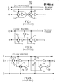
- FIG. 1 A CMOS D-type dynamic flip-flop circuit of the prior art is shown in Figure 1 which requires both a N-channel MOS transistor Tl and a P-channel MOS transistor T2 in the master section and in the slave section. Due to this, a non-overlapping clock generator could not be used since the flip-flop circuit would be susceptible to the problem of feedthrough or racethrough. In another words, both of the P-channel transistors T2 would be partially turned on simultaneously whereby the data input would feed through to the successive stages. Thus, this prior art flip-flop circuit required the use of a specially-designed clock to insure proper transition time relative to the inverter delay. Further; this prior art circuit necessitated the routing of two lines to successive stages. In order to eliminate the routing of two lines, a flip-flop circuit of the prior art was constructed as shown in Figure 2. However, the circuit of Figure 2 required the use of an additional inverter gate 11 which increased its cost for manufacturing.
- FIG. 3 A CMOS D-type static flip-flop circuit of the prior art is shown in Figure 3.
- This circuit is similar to the dynamic flip-flop circuit of Figure 1 and requires the addition of a regeneration circuit formed of a N-channel MOS transistor T3, a P-channel MOS transistor T4 and an inverter gate 12 in both the master section and the slave section.
- the circuit of Figure 3 suffered from the same disadvantages of Figure 1 in that racethrough would occur if a non-overlapping clock generator was used.
- a flip-flop circuit of the prior art was constructed as shown in Figure 4. However, the circuit of Figure 4 required the generating and routing of four lines.
- CMOS D-type flip-flop circuits which are immune to the possibility of racethrough but is capable of utilizing a ⁇ standard or conventional non-overlapping clock generator.
- CMOS D-type flip-flop circuits which avoid the possibility of racethrough.
- CMOS D-type flip-flop circuit stage which permit the use of a two-phase non-overlapping clock generator for clocking both the master and slave sections so as to prevent inadvertent racethrough of data input to successive stages.
- CMOS D-type flip-flop circuit having a single N-channel MOS transistor for data transfer in a master section and in a slave section for use as a dynamic shift register.
- CMOS D-type flip-flop circuit having a single N-channel MOS transistor for data transfer in a master section and in a slave section for use as a static shift register.
- CMOS D-type flip-flop circuit for use as an input data multiplexer.
- CMOS D-type flip-flop circuit for receiving an output from a N-channel FET array.
- the present invention is concerned with the provision of a CMOS D-type flip-flop circuit which avoids the possibility of feedthrough which includes a non-overlapping clock generator section having a true clock output and a complement clock output.
- the flip-flop circuit includes a master section formed of a first transfer gate, a first regenerative transistor and a first inverter gate.
- the first transfer gate is formed of a first N-channel MOS transistor
- the regenerative transistor is formed of a first P-channel MOS transistor.
- the N-channel transistor has one of its common electrodes connected to a D input terminal, its other common electrode connected to the input of the first inverter gate and its gate electrode connected to the complement clock output.
- the first P-channel transistor has one of its common electrodes connected to a supply potential, its other common electrode connected to the input of the first inverter gate and its gate electrode connected to the output of the first inverter gate.
- the flip-flop circuit further includes a slave section formed of a second transfer gate, a second regenerative transistor and a second inverter gate.
- the second transfer gate is formed of a second N-channel MOS transistor
- the 'second regenerative transistor is formed of a second P-channel MOS transistor.
- the second N-channel transistor has one of its common electrodes connected to the output of the first inverter gate, its other common electrode connected to the input of the second inverter gate and its gate electrode connected to the true clock output.
- the second.P-channel transistor has one of its common electrodes connected to the supply potential, its other common electrode connected to the input of the second inverter gate and its gate electrode connected.to the output of the second inverter gate and to an output terminal.
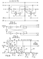
- FIG. 6 a schematic circuit diagram of a CMOS D-type dynamic flip-flop circuit 10 of the present invention which is employed for use as a data or shift register stage.
- dynamic refers to a clock generator which is continually changed between a high or logic "1" state and a low or logic "0" state.
- a dynamic flip-flop circuit is one which is adapted to receive such a clock generator.
- the flip-flop circuit 10 is formed of a master section 12, a slave section 14 and a clock generator section 16.
- the master section 12 includes a transfer gate formed of a single N-channel MOS transistor 18, a regenerative transistor formed of a P-channel MOS transistor 20 and an inverter gate 22.
- One of the common electrodes such as the source electrode of the transistor 18 is connected to a D input terminal 24 for receiving data input signals.
- the drain electrode of the transistor 18 is connected to the source of the transistor 20 and to the input of the inverter gate 22.
- the gate electrode of the transistor 18 is connected to a first or false clock output signal C from the clock generator 16.
- the drain electrode of the transistor 20 is connected to a supply voltage or potential VCC.
- the gate electrode of the transistor 20 is connected to the output of the inverter gate 22 which is defined as the output of the master section 12.
- the slave section 14 is identical in construction to the master section 12 and includes a transfer gate formed of a single N-channel MOS transistor 26, a regenerative transistor formed of a P-channel MOS transistor 28 and an inverter gate 30.
- the source electrode of the transistor 26 is connected to the output (node A) of the master section 12.
- the drain electrode of the transistor 26 is connected to the source of the transistor 28 and to the input of the inverter gate 30.
- the gate electrode of the transistor 26 is connected to a second or true clock signal C from the clock generator section 16.
- the drain electrode of transistor 28 is connected to the supply potential VCC.
- the gate electrode of the transistor 28 is connected to the output of the inverter gate 30 which is defined as the output of the slave section 14 or as the Q-output on output terminal 31 of the flip-flop circuit.
- the regenerative transistor p0 in the master section serves to pull up the input to the transfer gate 18 so that the voltage at the output of the inverter gate 22 will be near the supply potential VCC.
- the supply potential VCC for CMOS circuits is +5 volts.
- the regenerative transistor 28 in the slave section serves to pull up the input to the transfer gate 26 so that the output of the inverter gate 30 will also be near the supply potential VCC.
- the clock generator section 16 is formed of a pair of NOR gates 32, 34 and an inverter gate 36.
- the first NOR gate 32 has its one input connected to an input terminal 38 for receiving a clock input signal and to the input of the inverter gate 36.
- the other input of the NOR gate 32 is connected to the output of the second NOR gate 34.
- the output of the NOR gate 32 is connected to a first input of the second NOR gate 34.
- the other input of the NOR gate 34 is connected to the output of the inverter gate 36.
- the output of the NOR gate 34 on line 40 provides a true clock output signal C
- the output of the NOR gate 32 on line 42 provides a false or complement clock output signal C.
- These clock output signals C and C define the respective master and slave clock outputs of a two-phase non-overlapping clock generator wherein one of the outputs is in a low or logic "0" state and the other output is in a high or logic "1" state.
- the complement clock output signal ? is fed to the gate electrode of the transistor 18 in the master section 12.
- the true clock output signal C is fed to the gate electrode.of the transistor 26 in the slave section 14.
- the master section and the slave section are connected together in the manner shown to form a first stage of the shift register.
- the complement clock output signal C is further connected to the gate electrode of the N-channel MOS transistor in each master section of the other successive stages.
- the true clock output signal C is further connected to the gate electrode of the N-channel MOS transistor in each slave section of the other successive stages.
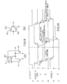
- the master section will have sampled the data input signal (Fig. lOa) which is assumed to be in a logic "1" state at time tl.
- the data input signal on the D input on terminal 24 will be transferred to the output or node A (Fig. 10e) of the master section immediately prior to the clock input signal making a transition.
- the clock input signal makes a transition from the logic "0" state to a logic "1” state
- the complement clock output signal C will be switched to a low level or logic "0” state while the true clock output signal C is still in the logic "0” state since the pull down transition in FET circuits is faster than the pull up transition.
- the transistor 18 will now be turned off so that the master section 12 will be latched to store the state of the D input or logic "1". This occurs at the time t2. Subsequently, the true clock output signal C will be switched at the time t3 to the logic "1" state at a short delay time after the complement clock output signal C has been already in the logic "0" state. Under this condition, the output of the master section 12 at node A will be transferred to the Q output (Fig. 10f) of the slave section 14 since the transistor 26 will be turned on.
- the true clock output signal C When the input signal makes a transition from the logic "0" state to a logic “0” state, the true clock output signal C will be switched to a low level or logic “0” state while the complement clock output signal C is still in the logic “0” state due to the faster pull down action in the FET circuits. Thus, the transistor 26 will be turned off again so as to latch the output of the slave section 14, which is also the Q output of the flip-flop circuit. This occurs at the time t4. Subsequently, the complement clock output signal C will be switched at the time t5 to the logic "1" state at a short delay time after the true clock output signal C has been already in the logic "0" state.
- next or new data input signal will be sampled and loaded or transferred to the node A of the master section.
- the new data input signal will now be ready for transfer to the slave section when the next clock input signal makes again a transition from the logic "0" state to the logic "1" state.
- a similiar operation will occur in which the data input signal on the D inputs at the successive stages will be transferred to the respective Q outputs.
- both the transistor 18 in the master section and the transistor 26 in the slave section turned on simultaneously. Since both of the transistors are made to be in the non-conductive state before one of them is allowed to be rendered conductive, this guarantees that there will be no inadvertent racethrough or feedthrough of the D input due to the overlapping of conduction of both transistors in the master and slave sections.
- the D input would ripple through the first stage and to all of the successive stages creating an erroneous reading in the shift register since the D input terminal in each successive stage is connected to the Q output of the preceding stage.
- FIG 7 there is illustrated a schematic circuit diagram of a CMOS static D-type flip-flop circuit 44 of the present invention.
- the term “static” refers to a clock generator which can remain indefinitely either in the logic "1" state or logic "0" state.
- a static flip-flop is one which is adapted for receiving such a clock signal.
- the flip-flop circuit 44 is formed of a master section 46, a slave section 48 and a clock generator section 50.
- the master section 46 includes a transfer gate formed of a single N-channel MOS transistor 52, a regenerative transistor formed of a P-channel MOS transistor 54, an inverter gate 56 and a regeneration circuit 58.
- the source electrode of the transistor 52 is connected to a D input terminal 53 for receiving data input 'signals.
- the drain electrode of the transistor 52 is connected to the source of the transistor 54 and to the input inverter gate 56.
- the gate of the transistor 52 is connected to a first or false clock output signal C from the clock generator 50.
- the drain electrode of the transistor 54 is connected to a supply voltage or potential VCC.
- the gate of the transistor 54 is connected to the output of the inverter gate 56 which is defined as the output of the master section 46.
- the regeneration circuit 58 is formed of an inverter gate 60 and a N-channel MOS transistor 62.
- the input of the inverter gate 60 is connected to the output of the master section which is at the output of the inverter gate 56 or node A.
- the source of the transistor 62 is connected to the output of the inverter gate 60.
- the drain of the transistor 62 is connected to the input of the inverter gate 56.
- the gate electrode of the transistor 62 is connected to a second or true clock output signal C from the clock generator section 50.
- the input of the inverter gate 60 defines a first input of the regeneration circuit 58, and the gate electrode of the transistor 62 defines a second input of the circuit 58.
- the drain of the transistor 62 defines an output of the circuit 58.
- the slave section 48 is identical in construction to the master section and comprises a transfer gate formed of a single N-channel MOS transistor 64, a regenerative transistor formed of a P-channel MOS transistor 66 and inverter gate 68 and a regeneration circuit 70.
- the source electrode of the transistor 64 is connected to the output (node A) of the master section 46.
- the drain electrode of the transistor 64 is connected to the source of the transistor 66 and to the input of the inverter gate 68.
- the gate electrode of the transistor 64 is connected to the second or true clock output signal C from the clock generator section 50.
- the drain electrode of the transistor 66 is connected to the supply potential VCC.
- the gate electrode of the transistor 66 is connected to the output of the inverter gate 68 which is defined as the output of the slave section 48 or as the Q output on output terminal 73 of the flip-flop circuit.
- the regeneration circuit 70 is formed of an inverter gate 69 and a N-channel MOS transistor 71.
- the input of the inverter gate 69 is connected to the output of the slave section which is at the output of the inverter gate 68 or the Q output on the terminal 73.
- the source of the transistor 71 is connected to the output of the inverter gate 69.
- the drain electrode of the transistor 71 is connected to the input of the inverter gate 68.
- the gate electrode of the transistor 71 is connected to the false clock output signal C from the clock generator circuit section 50.
- the input of the inverter gate 69 defines a first input of the regeneration circuit 70, and the gate electrode of the transistor 71 defines a second input of the circuit 70, The drain of the transistor 71 defines an output of the circuit 70.
- the clock generator section 50 is identical to the clock generator section 16 of Figure 6. Thus, no further description of the components and their operation is deemed to be necessary. However, it should be noted that this is a static clock generator where the clock input signal on the terminal 38 may remain in either the high state or the low state indefinitely. Therefore, the true clock output signal C will remain in a high or low state indefinitely. The complement or false clock output signal C will assume the opposite state to the true clock output C.
- the N-channel transistor 62 in the regeneration circuit 58 of the master section 46 will be turned on and the transistor 71 in the slave section 48 will be turned off.
- the output of the inverter gate 56 in the master section will be sent back to its input through the inverter gate 60 and the transistor 62 so as to cause latching thereof.
- the N-channel transistor 71 in the regeneration circuit 70 of the slave section 48 will be turned on and the transistor 62 in the master section will be turned off.
- FIG. 8 of the drawings there is shown a schematic circuit diagram of a CMOS D-type flip-flop circuit 72 of the present invention which is employed for use as an input data multiplexer.
- the flip-flop circuit is formed of a master section 74, a slave section 76 and a clock generator section 78.
- the master section 74 consists of a plurality of multiplexed data. input transistors each formed of a N-channel MOS transistor 80, 81, a regenerative transistor formed of a P-channel MOS transistor 82 and an inverter gate 84.
- the source electrode of the transistor 80 is connected to an input data terminal for receiving data signal A.
- the drain electrode of the transistor 80 is connected to a source of the transistor 82 and to the input of the inverter gate 84.
- the gate electrode of the transistor 80 is connected to a first master clock output signal CMA from the clock generator section 78.
- the drain electrode of the transistor 82 is connected to a supply voltage or potential VCC.
- the gate electrode of the transistor 82 is connected to the output of the inverter gate 84 which is defined as the output of the master section 74.
- the transistor 81 is connected similarly to the transistor 80.
- the source electrode of the transistor 81 is connected to an input data terminal for receiving data signal B.
- the drain electrode of the transistor 81 is connected to the drain of the transistor 80.
- the gate electrode of the transistor 81 is connected to the second master clock output signal CMB of the clock generator circuit section 78. While only two data input transistors have been shown, it should be clearly understood that a number of additional transistors could be similarly connected.
- the slave section 76 consists of a transfer gate formed of a single N-channel MOS transistor 86, a regenerative transistor 88 and an inverter gate 90.
- the source electrode of the transistor 86 is connected to the output (node A) of the master section 74.
- the drain of the transistor 86 is connected to the source of the transistor 88 and to the input of the inverter gate 90.
- the gate electrode-of the transistor 86 is connected to a slave clock output signal CS from the clock generator section 78.
- the drain electrode of the transistor 88 is connected to the supply potential VCC.
- a gate of the transistor 88 is connected to the output of the inverter gate 90 which is defined as the output of the slave section 76 or as output terminal 91 of the flip-flop circuit.
- the clock generator section 78 is a slightly modified version of the clock generator section 16 and comprises three NOR gates 32a, 34a, 33 and two inverter gates 36a, 37.
- the NOR gates 32a and 33 each have one of its inputs connected to an input terminal 38a for receiving a clock input signal and to the input of the inverter gate 36a.
- a second input of each NOR gates 32a and 33 is connected to the output of the NOR gate 34a.
- the third input of the NOR gate 32a is conhected to a control signal X for selecting either data signal A or data signal B.
- the control signal X is fed to the input of the inverter 37 whose output is joined to the third input the NOR gate 33.
- the outputs of the inverter gate 36a, the NOR gate 32a, and the NOR gate 33 are the three inputs to the NOR gate 34a.
- the output of the NOR gate 34a defines the slave clock output and is fed to the gate electrode of the transistor 86 in the slave section 76.
- the output of the NOR gate 33 defines the first master clock output and is fed to the gate electrode of data input transistor 80.
- the output of the NOR gate 32a defines the second master clock output and is fed to the gate electrode of data input transistor 81. Except for these differences in the clock generator 78, the manner and operation of the flip-flop circit 72 in transferring either the selected data signal A or data signal B dependent upon the control signal X will be identical to what was previously explained in connection with figures 6 and 10(a) through (f).
- Figures 9(a) and 9(b) the details of the logical representations of the NOR gates and inverter gates in Figures 6, 7 and 8 are illustrated in Figures 9(a) and 9(b).
- the NOR gate of Figure 9(a) is formed of a pair of P-channel MOS transistors Pl, P2 and a pair of N-channel MOS transistors N1, N2.
- the inverter gate of Figure 9(b) is formed of a P-channel MOS transistor P3 and a N-channel MOS transistor N3. It should be apparent to those skilled in the art that the N-channel transistor could be replaced by a P-channel transistor and vice versa in the master and slave sections of Figures 6, 7 and 8.
- the present invention provides an improved CMOS D-type flip-flop circuit which avoids the possibility of feedthrough.
- a single N-channel MOS transistor is used as a transfer gate in a master section and in a slave section which permits the use of a two-phase non-overlapping clock generator.
Landscapes
- Static Random-Access Memory (AREA)
- Shift Register Type Memory (AREA)
- Semiconductor Memories (AREA)
- Manipulation Of Pulses (AREA)
- Logic Circuits (AREA)
Applications Claiming Priority (2)
| Application Number | Priority Date | Filing Date | Title |
|---|---|---|---|
| US717350 | 1985-03-29 | ||
| US06/717,350 US4691122A (en) | 1985-03-29 | 1985-03-29 | CMOS D-type flip-flop circuits |
Publications (2)
| Publication Number | Publication Date |
|---|---|
| EP0196894A2 true EP0196894A2 (de) | 1986-10-08 |
| EP0196894A3 EP0196894A3 (de) | 1987-09-02 |
Family
ID=24881666
Family Applications (1)
| Application Number | Title | Priority Date | Filing Date |
|---|---|---|---|
| EP86302332A Withdrawn EP0196894A3 (de) | 1985-03-29 | 1986-03-27 | CMOS-D-Flip-Flop-Schaltungen |
Country Status (3)
| Country | Link |
|---|---|
| US (1) | US4691122A (de) |
| EP (1) | EP0196894A3 (de) |
| JP (1) | JPH0693608B2 (de) |
Cited By (2)
| Publication number | Priority date | Publication date | Assignee | Title |
|---|---|---|---|---|
| EP0277767A3 (en) * | 1987-02-04 | 1989-10-04 | American Telephone And Telegraph Company | Dynamic cmos current surge control |
| DE19654928C2 (de) * | 1995-09-05 | 2001-02-01 | Mitsubishi Electric Corp | Speicherschaltung |
Families Citing this family (31)
| Publication number | Priority date | Publication date | Assignee | Title |
|---|---|---|---|---|
| US4837465A (en) * | 1985-01-16 | 1989-06-06 | Digital Equipment Corp | Single rail CMOS register array and sense amplifier circuit therefor |
| JPS63136815A (ja) * | 1986-11-28 | 1988-06-09 | Mitsubishi Electric Corp | 周期信号発生回路 |
| US4804864A (en) * | 1987-03-09 | 1989-02-14 | Rockwell International Corporation | Multiphase CMOS toggle flip-flop |
| JPH07112147B2 (ja) * | 1989-11-13 | 1995-11-29 | 三菱電機株式会社 | 半導体集積回路 |
| US5239206A (en) * | 1990-03-06 | 1993-08-24 | Advanced Micro Devices, Inc. | Synchronous circuit with clock skew compensating function and circuits utilizing same |
| US5140180A (en) * | 1990-08-24 | 1992-08-18 | Ncr Corporation | High speed cmos flip-flop employing clocked tristate inverters |
| US5086236A (en) * | 1990-08-27 | 1992-02-04 | Advanced Micro Devices, Inc. | Synchronizing circuit of two clock signals |
| US5291070A (en) * | 1991-01-28 | 1994-03-01 | Advanced Micro Devices, Inc. | Microprocessor synchronous timing system |
| US5126596A (en) * | 1991-03-18 | 1992-06-30 | Motorola, Inc. | Transmission gate having a pass transistor with feedback |
| JP3087355B2 (ja) * | 1991-07-15 | 2000-09-11 | 日本電気株式会社 | デルタシグマ変調器 |
| JPH0528789A (ja) * | 1991-07-25 | 1993-02-05 | Sharp Corp | 論理回路 |
| US5638542A (en) * | 1993-12-29 | 1997-06-10 | Intel Corporation | Low power non-overlap two phase complementary clock unit using synchronous delay line |
| US5491441A (en) * | 1994-06-30 | 1996-02-13 | International Business Machines Corporation | Method and apparatus for generating a clock signal from a continuous oscillator signal including a translator circuit |
| DE69533604T2 (de) * | 1994-07-05 | 2005-02-10 | Matsushita Electric Industrial Co., Ltd., Kadoma | Verriegelungsschaltung |
| US5767716A (en) * | 1995-09-26 | 1998-06-16 | Texas Instruments Incorporated | Noise insensitive high performance energy efficient push pull isolation flip-flop circuits |
| JP3530422B2 (ja) * | 1999-06-16 | 2004-05-24 | Necエレクトロニクス株式会社 | ラッチ回路とレジスタ回路 |
| US20020000858A1 (en) | 1999-10-14 | 2002-01-03 | Shih-Lien L. Lu | Flip-flop circuit |
| GB2361121A (en) * | 2000-04-04 | 2001-10-10 | Sharp Kk | A CMOS LCD scan pulse generating chain comprising static latches |
| JP2002208841A (ja) * | 2001-01-11 | 2002-07-26 | Seiko Instruments Inc | ダイナミックフリップフロップ |
| JP2005518699A (ja) * | 2002-02-21 | 2005-06-23 | コーニンクレッカ フィリップス エレクトロニクス エヌ ヴィ | 低減された基板バウンスを有する集積回路 |
| JP2004056454A (ja) * | 2002-07-19 | 2004-02-19 | Seiko Instruments Inc | フリップフロップとシフトレジスタ及びその動作方法 |
| KR100526350B1 (ko) * | 2003-08-23 | 2005-11-08 | 삼성전자주식회사 | 다상 클록신호 발생회로 및 방법 |
| US20060013352A1 (en) * | 2004-07-13 | 2006-01-19 | Ching-Wei Lin | Shift register and flat panel display apparatus using the same |
| KR100624115B1 (ko) * | 2005-08-16 | 2006-09-15 | 삼성에스디아이 주식회사 | 유기전계발광장치의 발광제어 구동장치 |
| KR102116722B1 (ko) | 2013-10-16 | 2020-06-01 | 삼성전자 주식회사 | 반도체 회로 및 반도체 시스템 |
| US9618580B2 (en) * | 2015-05-07 | 2017-04-11 | International Business Machines Corporation | Debugging scan latch circuits using flip devices |
| US9805772B1 (en) * | 2016-10-20 | 2017-10-31 | Micron Technology, Inc. | Apparatuses and methods to selectively perform logical operations |
| US10340898B1 (en) * | 2017-06-23 | 2019-07-02 | Xilinx, Inc. | Configurable latch circuit |
| US11218137B2 (en) * | 2020-04-14 | 2022-01-04 | Globalfoundries U.S. Inc. | Low clock load dynamic dual output latch circuit |
| US12278624B2 (en) * | 2022-02-11 | 2025-04-15 | Pratt & Whitney Canada Corp. | Logic circuit for providing a signal value after a predetermined time period and method of using same |
| US20250253834A1 (en) * | 2024-02-05 | 2025-08-07 | Taiwan Semiconductor Manufacturing Company, Ltd. | Single Phase Clock Controlled Master Latch in Flip Flops |
Family Cites Families (7)
| Publication number | Priority date | Publication date | Assignee | Title |
|---|---|---|---|---|
| US4409671A (en) * | 1978-09-05 | 1983-10-11 | Motorola, Inc. | Data processor having single clock pin |
| US4356411A (en) * | 1978-12-12 | 1982-10-26 | Tokyo Shibaura Denki Kabushiki Kaisha | Flip-flop circuit |
| US4390987A (en) * | 1981-07-14 | 1983-06-28 | Rockwell International Corporation | Multiple input master/slave flip flop apparatus |
| JPS58184822A (ja) * | 1982-03-31 | 1983-10-28 | Fujitsu Ltd | 入力回路 |
| US4484087A (en) * | 1983-03-23 | 1984-11-20 | General Electric Company | CMOS latch cell including five transistors, and static flip-flops employing the cell |
| US4598214A (en) * | 1983-10-31 | 1986-07-01 | Texas Instruments Incorporated | Low power shift register latch |
| JPS61161826A (ja) * | 1985-01-11 | 1986-07-22 | Nec Corp | 相補型misfetを用いたラツチ回路 |
-
1985
- 1985-03-29 US US06/717,350 patent/US4691122A/en not_active Expired - Lifetime
-
1986
- 1986-03-27 EP EP86302332A patent/EP0196894A3/de not_active Withdrawn
- 1986-03-28 JP JP61072379A patent/JPH0693608B2/ja not_active Expired - Fee Related
Cited By (2)
| Publication number | Priority date | Publication date | Assignee | Title |
|---|---|---|---|---|
| EP0277767A3 (en) * | 1987-02-04 | 1989-10-04 | American Telephone And Telegraph Company | Dynamic cmos current surge control |
| DE19654928C2 (de) * | 1995-09-05 | 2001-02-01 | Mitsubishi Electric Corp | Speicherschaltung |
Also Published As
| Publication number | Publication date |
|---|---|
| EP0196894A3 (de) | 1987-09-02 |
| JPS6236913A (ja) | 1987-02-17 |
| US4691122A (en) | 1987-09-01 |
| JPH0693608B2 (ja) | 1994-11-16 |
Similar Documents
| Publication | Publication Date | Title |
|---|---|---|
| US4691122A (en) | CMOS D-type flip-flop circuits | |
| US4442508A (en) | Storage cells for use in two conductor data column storage logic arrays | |
| US4568842A (en) | D-Latch circuit using CMOS transistors | |
| US4114049A (en) | Counter provided with complementary field effect transistor inverters | |
| US5777491A (en) | High-performance differential cascode voltage switch with pass gate logic elements | |
| US5400295A (en) | Semiconductor integrated circuit device and semiconductor memory device | |
| CA1157111A (en) | Dynamic ratioless circuitry for random logic applications | |
| KR860009427A (ko) | 2-위상 클록신호 공급 쉬프트 레지스터형 반도체 메모리장치 | |
| US4990800A (en) | Mode selector for use in semiconductor memory device | |
| JPS61262314A (ja) | Cmos技術による静的双安定フリツプフロツプ回路 | |
| KR910006510B1 (ko) | 반도체집적회로 | |
| US4101790A (en) | Shift register with reduced number of components | |
| US5936449A (en) | Dynamic CMOS register with a self-tracking clock | |
| US4420695A (en) | Synchronous priority circuit | |
| US3708688A (en) | Circuit for eliminating spurious outputs due to interelectrode capacitance in driver igfet circuits | |
| EP0147103B1 (de) | MOS-Durchführung eines Schieberegisterverrieglers | |
| US4599528A (en) | Self booting logical or circuit | |
| US4856034A (en) | Semiconductor integrated circuit | |
| US3813563A (en) | Flip-flop circuit | |
| JPH0576120B2 (de) | ||
| US4771187A (en) | Bistable circuit | |
| US6172527B1 (en) | Output circuit capable of reducing feedthrough current | |
| US3609406A (en) | Integrated circuit inverter | |
| JPH07221605A (ja) | ラッチ回路並びにそれを用いたレジスタ回路およびパイプライン処理回路 | |
| JP3235105B2 (ja) | 演算回路 |
Legal Events
| Date | Code | Title | Description |
|---|---|---|---|
| PUAI | Public reference made under article 153(3) epc to a published international application that has entered the european phase |
Free format text: ORIGINAL CODE: 0009012 |
|
| AK | Designated contracting states |
Kind code of ref document: A2 Designated state(s): AT BE CH DE FR GB IT LI LU NL SE |
|
| PUAL | Search report despatched |
Free format text: ORIGINAL CODE: 0009013 |
|
| AK | Designated contracting states |
Kind code of ref document: A3 Designated state(s): AT BE CH DE FR GB IT LI LU NL SE |
|
| 17P | Request for examination filed |
Effective date: 19871014 |
|
| 17Q | First examination report despatched |
Effective date: 19890413 |
|
| STAA | Information on the status of an ep patent application or granted ep patent |
Free format text: STATUS: THE APPLICATION IS DEEMED TO BE WITHDRAWN |
|
| 18D | Application deemed to be withdrawn |
Effective date: 19901030 |
|
| RIN1 | Information on inventor provided before grant (corrected) |
Inventor name: SCHNIZLEIN, PAUL G. Inventor name: TANG, WEN-TSUNG FRED |