EP0197501A2 - Ausgedehntes Drain-Konzept für einen verminderten Hochgeschwindigkeitselektroneneffekt - Google Patents
Ausgedehntes Drain-Konzept für einen verminderten Hochgeschwindigkeitselektroneneffekt Download PDFInfo
- Publication number
- EP0197501A2 EP0197501A2 EP86104512A EP86104512A EP0197501A2 EP 0197501 A2 EP0197501 A2 EP 0197501A2 EP 86104512 A EP86104512 A EP 86104512A EP 86104512 A EP86104512 A EP 86104512A EP 0197501 A2 EP0197501 A2 EP 0197501A2
- Authority
- EP
- European Patent Office
- Prior art keywords
- transistor
- semiconductor body
- doped
- dopant
- approximately
- Prior art date
- Legal status (The legal status is an assumption and is not a legal conclusion. Google has not performed a legal analysis and makes no representation as to the accuracy of the status listed.)
- Withdrawn
Links
Images
Classifications
-
- H—ELECTRICITY
- H10—SEMICONDUCTOR DEVICES; ELECTRIC SOLID-STATE DEVICES NOT OTHERWISE PROVIDED FOR
- H10D—INORGANIC ELECTRIC SEMICONDUCTOR DEVICES
- H10D30/00—Field-effect transistors [FET]
- H10D30/01—Manufacture or treatment
- H10D30/021—Manufacture or treatment of FETs having insulated gates [IGFET]
- H10D30/0223—Manufacture or treatment of FETs having insulated gates [IGFET] having source and drain regions or source and drain extensions self-aligned to sides of the gate
- H10D30/0227—Manufacture or treatment of FETs having insulated gates [IGFET] having source and drain regions or source and drain extensions self-aligned to sides of the gate having both lightly-doped source and drain extensions and source and drain regions self-aligned to the sides of the gate, e.g. lightly-doped drain [LDD] MOSFET or double-diffused drain [DDD] MOSFET
-
- H—ELECTRICITY
- H10—SEMICONDUCTOR DEVICES; ELECTRIC SOLID-STATE DEVICES NOT OTHERWISE PROVIDED FOR
- H10D—INORGANIC ELECTRIC SEMICONDUCTOR DEVICES
- H10D30/00—Field-effect transistors [FET]
- H10D30/60—Insulated-gate field-effect transistors [IGFET]
- H10D30/601—Insulated-gate field-effect transistors [IGFET] having lightly-doped drain or source extensions, e.g. LDD IGFETs or DDD IGFETs
Definitions
- the present invention relates to field effect transistor devices and more particularly, to such devices containing differentially doped subsurface structures which provide reduced electric field strength levels at the interface boundary between the gate oxide and the semiconductor body.
- MOSFET metal-oxide-semiconductor
- This component of electric field is parallel to the interface between the silicon semiconductor and the silicon oxide insulating layer beneath the gate electrode. Energetic electrons tend to surmount the silicon/silicon-oxide energy barrier and are trapped within the oxide gate insulator or generate undesirable interface states by mechanisms which are not yet fully understood.
- Hot or energetic electrons from the channel current have a tendency to acquire sufficient energy to surmount the barrier between the semiconductor and the gate oxide and as a result, are injected into the oxide. Subsequent trapping of the injected electrons tends to cause device instabilities such as threshold-voltage shift and transconductance degradation. Accordingly, it is highly desirable that hot-electron resistant MOSFETs be devised to prevent such instabilities. These instabilities impose undesirably severe limitations on the further miniaturization of MOSFET devices in VLSI circuits.
- the hot electron problem is certainly undesirable and may eventually limit the minimum gate length for MOSFETs.
- improving the insulator quality with respect to hot electron trapping may be possible, most efforts at improving channel hot electron reliability have focused on reducing the lateral electric field strength within.the FET channel.
- Such attempts include graded source/drain junctions, double-diffused source/drain regions, and an oxide sidewall spacer adjacent to the gate electrode and oxide. All of these methods reduce the lateral field strength by making the n +- p drain-channel transition less abrupt.
- the instant inventors have found that the oxide sidewall spacer can increase'the maximum safe operating voltage by as much as 2 volts. A maximum gain of 1.5 volts per 1,000 angstroms of spacer length is possible. It is additionally noted that any method or structure which is directed at relieving the hot electron effect problem should be compatible with present VLSI semiconductor processing steps.
- a buried spacer is employed so as to move high density current flow away from the silicon/silicon-oxide interface boundary.
- a lightly doped region is developed by ion implantation in source or drain regions (preferably both) on either side of the gate electrode by means of a high voltage field. Silicon oxide spacers on either side of the gate electrode are then formed by a process such as reactive ion etching, which is anisotropic.
- a second ion implantation operation is performed at an increased dopant concentration, but at a lower ion implant field strength.
- the higher dopant concentrations result in deeper semiconductor penetration.
- more lightly doped regions extend from the source and drain regions beneath the semiconductor surface. It is between these two source and drain extensions that the highest current density is most likely achieved. This results in a reduction of hot electron production in the vicinity of the gate oxide.
- the lateral electric field strength, particularly the field strength immediately beneath the gate oxide, is significantly reduced.
- Figure 1 illustrates an NMOSFET device in accordance with the present invention. Except for the specific processing employed to carry out the purposes of the present invention, device fabrication is accomplished in the conventional fashion.
- Figure 1 particularly indicates an underlying n-doped substrate 99.
- field oxide layer 115 is grown on substrate 99 by exposing the substrate to oxygen at a high temperature, so as to form an insulating layer of silicon oxide 115. This layer is etched in a patterned fashion to define active areas on the chip or wafer.
- a p-doped well 100 is typically thereafter formed by ion implantation through the active area openings in the field oxide.
- a thin silicon oxide layer is then grown over the entire substrate.
- This oxide layer ultimately forms gate oxide 116 which comprises the structure which is subject to the hot electron trapping effect discussed above.
- a layer of polycrystalline silicon is deposited and heavily doped with an n-type dopant so as to provide a material exhibiting high electrical conductivity.
- This layer eventually forms gate electrode 130.
- metal rather than doped polycrystalline silicon may be employed for the gate electrode material.
- a mask is generally employed to produce gate electrode and electrode interconnection patterns where desired. These patterns are created by selective removal of the polycrystalline silicon or metal gate electrode material which typically leaves a thin oxide layer in the active area.
- n-type dopant such as arsenic or phosphorous is deposited in a buried layer. This deposition occurs by means of ion implantation at a voltage of approximately 200 keV. This results in the formation of lightly doped regions 103 and 104 (between the dotted lines) at a depth of approximately 1,000 angstroms below the silicon/oxide interface. It should be noted that regions 103 and 104 extend from field oxide 115 inwardly to the left and right edges of gate electrode 130. This doping is performed at an implant dosage of approximately 10 13 dopant atoms per square centimeter of source or drain region. In contrast, prior art doping process steps are carried out at much lower implantation voltages and do not produce the buried spacer effect described herein.
- another silicon dioxide layer is deposited on the surface of the wafer or chip.
- chemical vapor deposition is typically employed since it is desired to cover the entire surface of the device.
- a reactive ion etching step is then carried out, typically in an atmosphere of trifluoromethane (CHF 3 ) to anisotropically etch away most of this silicon layer except in those areas exhibiting sharp vertical transitions such as on either side of gate electrode 130.
- CHF 3 trifluoromethane
- the anisotropic etching is advantageous in that it leaves oxide spacers 117' on either side of gate electrodes 130.
- spacers 117' also provide a form of self aligned mask for the next process step which is the ion implantation or diffusion of the source and drain regions.
- a heavier, n + , doping is applied to the source and drain regions of the active area.
- this second doping process step is performed at an implant dosage of about 8 x 10 15 dopant atoms per square centimeter.
- regions 101 and 102 in Figure 1 This results in the formation of regions 101 and 102 in Figure 1, these regions typically extending to a depth of between about 1,500 (150mm) and 4,000 angstroms. ecause of the masking effect produced by spacers 117', only a small n - doped region of the scurce and drain is left to extend inwardly from regions 101 and 102. Typically each gate side spacer 117' is between about 0.1 and 0.2 micrmeler in width. Accordingly, the lightly doped portions of the source and drain region extend inwardly toward the gate for a corresponding distance of between approximately 0.1 and 0.2 micrometer
- gate spacers 117' which comprise polysilicon material.
- lightly doped regions 103 and 104 can be implanted at more conventional voltage levels, say for example, 90 kev.
- buried channels are formed as the doped polysilicon or metal spacer is biased to a positive voltage via a doped polysilicon gate.
- reactive ion etching is employed to effect removal of the polycrystalline silicon material in the gate masking portion of the process.
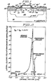
- Figure 2 illustrates the relative improvement in the lateral electric field in the gate region achieved by the various spacer configurations.
- Figure 2 illustrates computer simulated variations in electric field strength as a function of channel position. The electrical field strength is measured in megavolts per centimeter and the channel position is given in microns.
- the figure also indicates the various device regions across the gate region of the semiconductor material in a MOSFET device. More particularly, the figure illustrates the variation from the source to the drain region through the gate region and includes spacers on either side of the gate electrode. In all cases shown, the source-to-drain voltage, and the source to gate voltage was fixed at 5.5 volts.
- NMOSFETs of various channel lengths and widths in a boron-implanted p-doped semiconductor have been fabricated.
- the fabricated devices have included devices with and without oxide sidewall spacers.
- a light dose (typical- l y 10 12 to 10 14 atoms per square centimeter) of n-type ion implantation follows the gate etching step.
- An oxide layer is then conformally deposited and anisotropically etched to leave a sidewall remnant at all sharp steps, specifically at the gate electrode.
- the gate and sidewall oxide then act as a self-aligned mask for the conventional heavy source/drain ion implant or diffusion.
- the buried spacer concepts presented herein differs from conventional spacer structures principally in the ion implant energy of the light implant.
- the buried spacer implant is performed at a voltage level of 200 keV while the conventional spacer and the source/drain were implanted at 90 keV.
- the most direct assessment of the hot electron mitigation effect of the present invention is the measurement of device parameters before and after DC stress.
- inspection of the FET current voltage characteristics of this third device found no adverse consequences of the high energy spacer implant.
- the methods and structure of the present invention provide a viable solution to the problem of hot electron entrapment in the oxide layer of a MOSFET device. It is also seen that the present invention provides a simplified process for producing the desired structural implant modification without departing from conventional processing methodologies. It is also seen that the present invention permits the shrinkage of MOSFET circuits to densities which are even greater than those currently achievable without the necessity of scaling down supply voltages. Accordingly, devices manufactured in accordance with the present invention are much more readily incorporated in currently existing systems. It is also seen that the devices of the present invention are much better able to undergo voltage stress without significant device characteristic impairment.
- both the source and drain regions possess the buried channel structure of the present invention, it is possible to employ such a structure in only one of these regions. However, in transistors in which current flow is unidirectional it is generally preferred to employ such structures only in the drain region.
Landscapes
- Insulated Gate Type Field-Effect Transistor (AREA)
Applications Claiming Priority (2)
| Application Number | Priority Date | Filing Date | Title |
|---|---|---|---|
| US72264185A | 1985-04-12 | 1985-04-12 | |
| US722641 | 1985-04-12 |
Publications (2)
| Publication Number | Publication Date |
|---|---|
| EP0197501A2 true EP0197501A2 (de) | 1986-10-15 |
| EP0197501A3 EP0197501A3 (de) | 1986-12-17 |
Family
ID=24902729
Family Applications (1)
| Application Number | Title | Priority Date | Filing Date |
|---|---|---|---|
| EP86104512A Withdrawn EP0197501A3 (de) | 1985-04-12 | 1986-04-02 | Ausgedehntes Drain-Konzept für einen verminderten Hochgeschwindigkeitselektroneneffekt |
Country Status (3)
| Country | Link |
|---|---|
| EP (1) | EP0197501A3 (de) |
| JP (1) | JPS61259574A (de) |
| KR (1) | KR860008615A (de) |
Cited By (4)
| Publication number | Priority date | Publication date | Assignee | Title |
|---|---|---|---|---|
| DE3933194A1 (de) * | 1988-10-11 | 1990-04-12 | Mitsubishi Electric Corp | Halbleitereinrichtung mit verbesserten source- und drain-kontaktbereichen und verfahren zu deren herstellung |
| EP0198335B1 (de) * | 1985-04-12 | 1990-11-07 | General Electric Company | Gestaffeltes ausgedehntes Drain-Konzept für einen verminderten Hochgeschwindigkeitselektroneneffekt |
| EP0530644A3 (en) * | 1991-08-30 | 1993-08-04 | Texas Instruments Incorporated | Non-volatile memory cell and fabrication method |
| US5349225A (en) * | 1993-04-12 | 1994-09-20 | Texas Instruments Incorporated | Field effect transistor with a lightly doped drain |
Family Cites Families (5)
| Publication number | Priority date | Publication date | Assignee | Title |
|---|---|---|---|---|
| JPS5636585B2 (de) * | 1973-07-02 | 1981-08-25 | ||
| DE2834724A1 (de) * | 1978-08-08 | 1980-02-14 | Siemens Ag | Mos-feldeffekttransistoren fuer hoehere spannungen |
| JPS55136513A (en) * | 1979-04-13 | 1980-10-24 | Tanaka Atsuen Kiko:Kk | Knockout table of cooling bed |
| JPS58131773A (ja) * | 1982-02-01 | 1983-08-05 | Hitachi Ltd | 半導体装置の製造方法 |
| JPS59121878A (ja) * | 1982-12-28 | 1984-07-14 | Toshiba Corp | 半導体装置の製造方法 |
-
1986
- 1986-04-02 EP EP86104512A patent/EP0197501A3/de not_active Withdrawn
- 1986-04-07 JP JP61078413A patent/JPS61259574A/ja active Pending
- 1986-04-11 KR KR1019860002746A patent/KR860008615A/ko not_active Withdrawn
Cited By (7)
| Publication number | Priority date | Publication date | Assignee | Title |
|---|---|---|---|---|
| EP0198335B1 (de) * | 1985-04-12 | 1990-11-07 | General Electric Company | Gestaffeltes ausgedehntes Drain-Konzept für einen verminderten Hochgeschwindigkeitselektroneneffekt |
| DE3933194A1 (de) * | 1988-10-11 | 1990-04-12 | Mitsubishi Electric Corp | Halbleitereinrichtung mit verbesserten source- und drain-kontaktbereichen und verfahren zu deren herstellung |
| EP0530644A3 (en) * | 1991-08-30 | 1993-08-04 | Texas Instruments Incorporated | Non-volatile memory cell and fabrication method |
| US5264384A (en) * | 1991-08-30 | 1993-11-23 | Texas Instruments Incorporated | Method of making a non-volatile memory cell |
| US5482880A (en) * | 1991-08-30 | 1996-01-09 | Texas Instruments Incorporated | Non-volatile memory cell and fabrication method |
| US5646430A (en) * | 1991-08-30 | 1997-07-08 | Texas Instruments Incorporated | Non-volatile memory cell having lightly-doped source region |
| US5349225A (en) * | 1993-04-12 | 1994-09-20 | Texas Instruments Incorporated | Field effect transistor with a lightly doped drain |
Also Published As
| Publication number | Publication date |
|---|---|
| JPS61259574A (ja) | 1986-11-17 |
| EP0197501A3 (de) | 1986-12-17 |
| KR860008615A (ko) | 1986-11-17 |
Similar Documents
| Publication | Publication Date | Title |
|---|---|---|
| US4680603A (en) | Graded extended drain concept for reduced hot electron effect | |
| US4859620A (en) | Graded extended drain concept for reduced hot electron effect | |
| US6426279B1 (en) | Epitaxial delta doping for retrograde channel profile | |
| KR100473901B1 (ko) | SiGe층을포함하는반도체전계효과디바이스 | |
| EP0187016B1 (de) | MISFET mit niedrigdotiertem Drain und Verfahren zu seiner Herstellung | |
| US4613882A (en) | Hybrid extended drain concept for reduced hot electron effect | |
| US6391723B1 (en) | Fabrication of VDMOS structure with reduced parasitic effects | |
| US6221724B1 (en) | Method of fabricating an integrated circuit having punch-through suppression | |
| JP2546692B2 (ja) | Mosfetの製造方法 | |
| US5036017A (en) | Method of making asymmetrical field effect transistor | |
| US20010013628A1 (en) | Asymmetric mosfet devices | |
| EP0487220B1 (de) | SOI-Feldeffekttransistor und dessen Herstellungsverfahren | |
| US5536959A (en) | Self-aligned charge screen (SACS) field effect transistors and methods | |
| EP0493520B1 (de) | Misfet-anordnung mit abmessungen im submikrometerbereich und beseitigung der heissen ladungsträger | |
| US4454523A (en) | High voltage field effect transistor | |
| US4691433A (en) | Hybrid extended drain concept for reduced hot electron effect | |
| US6020611A (en) | Semiconductor component and method of manufacture | |
| US6030875A (en) | Method for making semiconductor device having nitrogen-rich active region-channel interface | |
| US4193182A (en) | Passivated V-gate GaAs field-effect transistor and fabrication process therefor | |
| US6150200A (en) | Semiconductor device and method of making | |
| EP0197501A2 (de) | Ausgedehntes Drain-Konzept für einen verminderten Hochgeschwindigkeitselektroneneffekt | |
| US5215936A (en) | Method of fabricating a semiconductor device having a lightly-doped drain structure | |
| KR100334968B1 (ko) | 매몰 채널 pmos 트랜지스터 제조 방법 | |
| KR940005453B1 (ko) | 반도체 트랜지스터의 제조방법 | |
| KR100239457B1 (ko) | 모오스 트랜지스터 제조방법 |
Legal Events
| Date | Code | Title | Description |
|---|---|---|---|
| PUAI | Public reference made under article 153(3) epc to a published international application that has entered the european phase |
Free format text: ORIGINAL CODE: 0009012 |
|
| AK | Designated contracting states |
Kind code of ref document: A2 Designated state(s): DE FR GB NL |
|
| PUAL | Search report despatched |
Free format text: ORIGINAL CODE: 0009013 |
|
| AK | Designated contracting states |
Kind code of ref document: A3 Designated state(s): DE FR GB NL |
|
| 17P | Request for examination filed |
Effective date: 19870603 |
|
| 17Q | First examination report despatched |
Effective date: 19881227 |
|
| STAA | Information on the status of an ep patent application or granted ep patent |
Free format text: STATUS: THE APPLICATION IS DEEMED TO BE WITHDRAWN |
|
| 18D | Application deemed to be withdrawn |
Effective date: 19890707 |
|
| RIN1 | Information on inventor provided before grant (corrected) |
Inventor name: PIMBLEY, JOSEPH MAXWELL Inventor name: WEI, CHING-YEU |