EP0197531A2 - Dünnfilmtransistor auf isolierendem Substrat - Google Patents
Dünnfilmtransistor auf isolierendem Substrat Download PDFInfo
- Publication number
- EP0197531A2 EP0197531A2 EP86104695A EP86104695A EP0197531A2 EP 0197531 A2 EP0197531 A2 EP 0197531A2 EP 86104695 A EP86104695 A EP 86104695A EP 86104695 A EP86104695 A EP 86104695A EP 0197531 A2 EP0197531 A2 EP 0197531A2
- Authority
- EP
- European Patent Office
- Prior art keywords
- film
- thin
- film transistor
- thin film
- transistor according
- Prior art date
- Legal status (The legal status is an assumption and is not a legal conclusion. Google has not performed a legal analysis and makes no representation as to the accuracy of the status listed.)
- Granted
Links
Images

Classifications
-
- H—ELECTRICITY
- H10—SEMICONDUCTOR DEVICES; ELECTRIC SOLID-STATE DEVICES NOT OTHERWISE PROVIDED FOR
- H10D—INORGANIC ELECTRIC SEMICONDUCTOR DEVICES
- H10D30/00—Field-effect transistors [FET]
- H10D30/01—Manufacture or treatment
- H10D30/021—Manufacture or treatment of FETs having insulated gates [IGFET]
- H10D30/031—Manufacture or treatment of FETs having insulated gates [IGFET] of thin-film transistors [TFT]
- H10D30/0312—Manufacture or treatment of FETs having insulated gates [IGFET] of thin-film transistors [TFT] characterised by the gate electrodes
- H10D30/0314—Manufacture or treatment of FETs having insulated gates [IGFET] of thin-film transistors [TFT] characterised by the gate electrodes of lateral top-gate TFTs comprising only a single gate
-
- H—ELECTRICITY
- H10—SEMICONDUCTOR DEVICES; ELECTRIC SOLID-STATE DEVICES NOT OTHERWISE PROVIDED FOR
- H10D—INORGANIC ELECTRIC SEMICONDUCTOR DEVICES
- H10D30/00—Field-effect transistors [FET]
- H10D30/01—Manufacture or treatment
- H10D30/021—Manufacture or treatment of FETs having insulated gates [IGFET]
- H10D30/031—Manufacture or treatment of FETs having insulated gates [IGFET] of thin-film transistors [TFT]
- H10D30/0321—Manufacture or treatment of FETs having insulated gates [IGFET] of thin-film transistors [TFT] comprising silicon, e.g. amorphous silicon or polysilicon
-
- H—ELECTRICITY
- H10—SEMICONDUCTOR DEVICES; ELECTRIC SOLID-STATE DEVICES NOT OTHERWISE PROVIDED FOR
- H10D—INORGANIC ELECTRIC SEMICONDUCTOR DEVICES
- H10D30/00—Field-effect transistors [FET]
- H10D30/60—Insulated-gate field-effect transistors [IGFET]
- H10D30/67—Thin-film transistors [TFT]
- H10D30/6729—Thin-film transistors [TFT] characterised by the electrodes
- H10D30/673—Thin-film transistors [TFT] characterised by the electrodes characterised by the shapes, relative sizes or dispositions of the gate electrodes
- H10D30/6731—Top-gate only TFTs
-
- H—ELECTRICITY
- H10—SEMICONDUCTOR DEVICES; ELECTRIC SOLID-STATE DEVICES NOT OTHERWISE PROVIDED FOR
- H10D—INORGANIC ELECTRIC SEMICONDUCTOR DEVICES
- H10D30/00—Field-effect transistors [FET]
- H10D30/60—Insulated-gate field-effect transistors [IGFET]
- H10D30/67—Thin-film transistors [TFT]
- H10D30/6729—Thin-film transistors [TFT] characterised by the electrodes
- H10D30/6737—Thin-film transistors [TFT] characterised by the electrodes characterised by the electrode materials
- H10D30/6739—Conductor-insulator-semiconductor electrodes
-
- H—ELECTRICITY
- H10—SEMICONDUCTOR DEVICES; ELECTRIC SOLID-STATE DEVICES NOT OTHERWISE PROVIDED FOR
- H10D—INORGANIC ELECTRIC SEMICONDUCTOR DEVICES
- H10D30/00—Field-effect transistors [FET]
- H10D30/60—Insulated-gate field-effect transistors [IGFET]
- H10D30/67—Thin-film transistors [TFT]
- H10D30/674—Thin-film transistors [TFT] characterised by the active materials
- H10D30/6741—Group IV materials, e.g. germanium or silicon carbide
- H10D30/6743—Silicon
- H10D30/6745—Polycrystalline or microcrystalline silicon
-
- H—ELECTRICITY
- H10—SEMICONDUCTOR DEVICES; ELECTRIC SOLID-STATE DEVICES NOT OTHERWISE PROVIDED FOR
- H10D—INORGANIC ELECTRIC SEMICONDUCTOR DEVICES
- H10D62/00—Semiconductor bodies, or regions thereof, of devices having potential barriers
- H10D62/80—Semiconductor bodies, or regions thereof, of devices having potential barriers characterised by the materials
- H10D62/83—Semiconductor bodies, or regions thereof, of devices having potential barriers characterised by the materials being Group IV materials, e.g. B-doped Si or undoped Ge
-
- H—ELECTRICITY
- H10—SEMICONDUCTOR DEVICES; ELECTRIC SOLID-STATE DEVICES NOT OTHERWISE PROVIDED FOR
- H10D—INORGANIC ELECTRIC SEMICONDUCTOR DEVICES
- H10D64/00—Electrodes of devices having potential barriers
- H10D64/60—Electrodes characterised by their materials
- H10D64/62—Electrodes ohmically coupled to a semiconductor
Definitions
- the present invention relates to a semiconductor device, and more particularly to a thin film thransistor formed on an insulating substrate.
- a thin film transistor (hereinafter referred to as "TFT") using a semiconductor film which is formed on an insulating substrate, is used for various purposes.
- TFT thin film transistor
- a circuit for operating the TFT's does not include the capacitance between the semiconductor film and an insulating sulstrate for supporting the semiconductor film, and hence the TFT's can operate at a higher speed, as compared with an integrated circuit which is formed in a bulk semiconductor substrate through the well-known separation technique using a pn junction.
- a thin film semiconductor device can be formed at a reduced temperature.
- a thin film transisotr array has been formed on a glass or quartz substrate, to be used in a liquid crystal display device.
- M. Matsui et al. J. Appl. Phys., Vol. 55, No. 6, 1984, pages 1590 through 1595.
- Such a prior art has drawbacks.
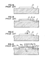
- a method of fabricating a conventional thin firlm semiconductor device by using the low-temperature process will be explained below, by reference to Figs. lA to 1D.
- a polycrystalline silicon film 2 having a thickness of 0.5 to 1 ⁇ m is formed on a glass substrate 1 by a chemical vapor deposition (CVD) method or the vacuum deposition method, and is selectively etched by photolithography so as to have the form of an island.
- CVD chemical vapor deposition
- a silicon oxide film 3 which has a thickness of about 2,000 A and serves as a gate insulating film, and a polycrystalline silicon film 4 which has a thickness of 0 about 5,000 A and serves as a gate material are formed by a CVD method.
- the silicon oxide film 3 and the gate polycrystalline silicon film 4 are selectively etched as shown in Fig. lC.
- a protective film 5 having a thickness of about 5,000 A is formed by a CVD method, and the structure thus obtained is then kept at 550°C for 10 hours, to activate phosphorous implanted in the silicon island 2 and to make the protective film 5 dense.
- the softening temperature of the glass substrate 1 is about 600°C. In order to carry out the above heat treatment without deforming the glass substrate 1, it is necessary to make the temperature of the heat treatment less than 600°C. Accordingly, it takes a lot of time to activate phosphorous implanted in the silicon island 2. Further, the use of the ion implantation method will increase the manufacturing cost of the device.
- n-type, highly-doped regions 6a and 6b serving as source and drain regions are completely formed by the above heat treatment, and will be kept in low-resistance contact with an electrode material.
- apertures for contact are formed in the protective film 5, and then a source electrode 7a and a drain electrode 7b each made of aluminium are deposited on the protective film 5, to be kept in contact with the source region 6a and the drain region 6b, respectively, through the apertures of the protective film 5.
- a TFT is completed.
- the cost for forming the source and drain regions becomes high, and moreover it takes a lot of time to activate implanted ions.
- An object of the present invention is to provide a TFT in which both a source region and a drain region can be formed without using the ion implantation method.
- Another object of the present invention is to provide a TFT in which both a source region and a drain region can be rapidly formed at a low temperature and at a low cost.
- a further object of the present invention is to provide a TFT in which both a source region and a drain region are formed by a self alignment manner.
- a TFT in which both a source region and a drain region are made of metal silicide.
- the resistance of a TFT in the OFF-state is determined by the inherent resistance of the channel region of the TFT, and the TFT is not always required to include a pn junction.
- both a source region and a drain region are made of metal silicide to reduce the resistivity of these regions.
- FIG. 2D An embodiment of a TFT according to the present embodiment will be explained below.
- the present embodiment has a MOS (namely, metal-oxide-semiconductor) structure, as shown in Fig. 2D.
- MOS metal-oxide-semiconductor
- a resist film 8 is formed on the gate polycrystalline silicon film 4 which is deposited on the silicon oxide film 3 as shown in Fig. 1B, and then the films 4 and 3 are selectively etched by photolithography. That is, the gate polycrystalline silicon film 4 is first etched by the plasma etching using carbon tetrafluoride (CF 4 ) and oxygen, and then the silicon oxide film 3 is etched by the plasma etching using trifluoromethane (CHF 3 ) and helium. Thus, the same structure as shown in Fig. lC is obtained.
- CF 4 carbon tetrafluoride
- CHF 3 trifluoromethane
- the polycrystalline silicon film 2 is then etched down by 0 a thickness of about 1,000 A through the plasma etching using carbon tetrafluoride and oxygen.
- the plasma etching using carbon tetrafluoride and oxygen can perform isotropic etching for silicon.
- the under cut is formed in the gate polycrystalline silicon film 4 underlying the resist film 8 and in that portion of the polycrystalline silicon film 2 which exists beneath the silicon oxide film 3, as shown in Fig. 2A.
- a 0 platinum layer 9 having a thickness of about 500 A is deposited as shown in Fig. 2B, by the evaporation from above. At this time, platinum is not deposited on that portion of the polycrystalline silicon film 2 where the above-mentioned under cut is formed, and hence the platinum layer on the gate polycrystalline silicon film 4 is separated from the platinum layer on the polycrystalline silicon film 2.
- the structure thus obtained is annealed in oxygen atmosphere at about 450°C for about 10 minutes, to form platinum silicide layers 10a to 10c as shown in Fig. 2C.
- the platinum silicide layers 10a to 10c are formed, the volume of each of these layers 10a to 10c is increased.
- the under cut existing beneath the silicon oxide film 3 is occupied by the platinum silicide layers 10a and lOb, and the surface of the semiconductor island 2 including the platinum silicide layers 10a and 10b is put in substratially the same plane as the bottom of the silicon oxide film 3.
- the platinum silicide layer 10c formed on the silicon oxide film 3 is separated by the film 3 from each of the platinum silicide layers 10a and 10b which serve as source and drain regions, respectively. That is, the short-circuiting between the platinum silicide layer 10c and each of the platinum silicide layers 10a and 10b never occurs.
- the gate, source and drain layers can be formed which are highly conductive and of self alignment type.
- the protective film 5 is then formed, and apertures for contact are formed in the protective film 5.
- the source and drain electrodes 7a and 7b each made of aluminium are deposited on the protective film 5, to be kept in ohmic contact with the silicide layers 10a and lOb, respectively, through the above apertures.
- the polycrystalline silicon film is used as the semiconductor active film.
- a monocrystalline silicon film or an amorphous silicon film may be used in place of the polycrystalline silicon film.
- the semiconductor film may be made of germanium, tellurium, or one of compound semiconductor materials such as cadmium selenide and gallium arsenide.
- platinum silicide is used as the metal silicide in the present embodiment, molybdenum, tungsten, titanium, palladium, mixtures of these metals or others may be used for making the metal silicide. In this case, the heat treatment at a temperature of 550 to 800°C is required to make the highly conductive metal silicide.
- the metal silicide can be made in a short time, without raising the temperature of the substrate.
- the glass substrate of the present embodiment may be replaced by a quartz substrate.
- the glass substrate may be replaced by semiconductor substrate coated with an insulating film. That is, it is essential that the substrate 1 acts as an insulator when viewed from the semiconductor film 2.
- the thin semiconductor film is made of polycrystalline silicon
- the gate portion is made of amorphous silicon.
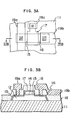
- a silicon island 12 formed of a thin polycrystalline silicon film is provided on an insulating substrate 11, and an amorphous silicon film 14, doped with an n-type impurity and hydrogen, is formed on a gate insulating film 13 which is provided on the silicon island 12.
- metal silicide layers 15 and 16 serving as source and drain regions are formed in the surface of the silicon island 12, and a metal silicide layer 17 is formed in the surface of the amorphous silicon film 14.
- the metal silicide layer 17 and the amorphous silicon film 14 serve as a gate electrode.
- a surface passivation film 18 is provided so as to cover the metal silicide layers 15 to 17, and through holes are formed in the surface passivation film 18, so that a source electrode 19a and a drain electrode 19b which are provided on the surface passivation film 18, are kept in ohmic contact with the source and drain regions, respectively, through the through holes.
- the gate insulating film 13 and the surface passivation film 18 are omitted for convenience' sake, and hatched portions indicate areas where the metal silicide layers 15, 16 and 17 are kept in ohmic contact with the source electrode 19a, the drain electrode 19b and gate wiring 19c, respectively.
- the source and drain regions formed of the metal silicide layers 15 and 16 are well bonded to the gate and drain electrodes 19a and 19b, respectively. Further, each of the source and drain regions has a low sheet resistivity in a lateral direction, and the series connection of the source and drain regions has a low resistance value. Further, even if those portions of the silicon island 2 where the metal silicide layers 15 and 16 are formed, are extended to form source wiring and drain wiring, the resistance of each of the source wiring and the drain wiring will not become too large.
- the gate electrode that is, the amophous silicon film 14 covered with the metal silicide layer 17 has a small sheet resistivity in a lateral direction, and may be extended to form the gate wiring 19c or to be connected to other TFT's.
- hydrogen contained in the amorphous silicon film 14 and polycrystalline silicon film 12 is unescapable, except the escape of hydrogen at the side surface of the gate insulating film 13. Accordingly, even if the heat treatment at a temperature exceeding 400°C is carried out, the bonding between silicon atoms and hydrogen atoms will be stable by the aid of the shielding hydrogen atom (dangling bonds being annihilated) and the resistance of the gate electrode will be kept at a low value. Further, the characteristics of the present embodiment scarcely vary with time. The above facts also hold in a case where the silicon island 12 is formed of a hydrogen-doped amorphous silicon film and a polycrystalline silicon film is used in place of the amorphous silicon film 14, to form the gate electrode.
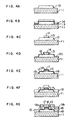
- a polycrystalline silicon film is deposited on the insulating substrate 11, and then shaped by photo-etching techniques so as to form the silicon island 12.
- the silicon oxide film 13 is deposited by a CVD method, to form the gate insulating film, and then the amorphous silicon film 14 doped with hydrogen and an n-type impurity is formed on the silicon oxide film 13 by a CVD method such as a plasma CVD method.
- a CVD method such as a plasma CVD method.
- the amorphous silicon 14 is selectively etched by photo-etching techniques, and then etching is performed for the silicon oxide film 13 while using the remaining amorphous silicon film as a mask, to remove the unwanted portion of the silicon oxide film 14.
- a metal layer 20 is deposited by the sputtering method or others, as shown in Fig. 4D.
- the heat treatment at a temperature of 200 to 500°C is carried out to cause the metal to react with silicon, thereby forming the metal silicide layers 15 to 17 as shown in Fig. 4E.
- the metal layer 20 on the side surface of the silicon oxide film 13 and the remaining metal layer 20 on the surface of the substrate 11 are removed by an acid.
- the surface passivation film 18 is made of silicon oxide, phosphosilicate glass, silicon nitride, or others, and then through holes are formed in the surface passivation film 18 by photo-etching techniques. Then, an electrode layer is formed on the surface passivation film 18 by the sputtering method or others, and patterning is carried out for the electrode layer by photo-etching techniques, to obtain the source electrode 19a and the drain electrode 19b as shown in Fig. 4G.
- a channel region of the silicon island 12 which exists beneath the gate insulating film 13 is hydrogenated by the heat treatment for making the metal silicide layers 15 to 17.
- additional heat treatment may be carried out at a more elevated temperature, to facilitate the diffusion of hydrogen into the silicon island 12.
- the silicon island 12 is made of polycrystalline silicon.
- an amorphous silicon film may be deposited on the insulating substrate 11, to form the silicon island 12, and a polycrystalline silicon film is deposited in place of the amorphous silicon film 14, to form the gate electrode.
- the present invention is applicable to a p-channel MOSFET and an n-channel MOSFET in each of which an impurity is diffused into those portions of the thin film 12 which are kept in contact with the source and drain electrodes.
- the whole of the silicon islands 12 except the channel region thereof may be occupied by the metal silicide.
- a metal for making the metal silicide may be one selected from a group consisting of platinum, molybdenum, tungsten, titanium palladium and mixtures of these metals.
- a TFT having a self alignment structure can be fabricated at a low temperature in a short time, and the sheet resistivity of the gate electrode can be reduced because the metal silicide layer is formed in the gate electrode.
- the polycrystalline silicon layer is hydrogenated by the heat treatment for forming the metal silicide layers, that is, can'be hydrogenated without increasing the number of fabricating steps. Even when additional heat treatment may be carried out after the heat treatment for forming the metal silicide layers has been completed, there is no fear of hydrogen excaping from a silicon film to the outside, and hence the TFT has stable characteristics.
Landscapes
- Thin Film Transistor (AREA)
Applications Claiming Priority (4)
| Application Number | Priority Date | Filing Date | Title |
|---|---|---|---|
| JP72636/85 | 1985-04-08 | ||
| JP60072636A JPS61231765A (ja) | 1985-04-08 | 1985-04-08 | 薄膜半導体装置の製造方法 |
| JP118811/85 | 1985-06-03 | ||
| JP60118811A JPS61278163A (ja) | 1985-06-03 | 1985-06-03 | 薄膜トランジスタの製造方法 |
Publications (3)
| Publication Number | Publication Date |
|---|---|
| EP0197531A2 true EP0197531A2 (de) | 1986-10-15 |
| EP0197531A3 EP0197531A3 (en) | 1989-06-14 |
| EP0197531B1 EP0197531B1 (de) | 1993-07-28 |
Family
ID=26413771
Family Applications (1)
| Application Number | Title | Priority Date | Filing Date |
|---|---|---|---|
| EP86104695A Expired - Lifetime EP0197531B1 (de) | 1985-04-08 | 1986-04-07 | Dünnfilmtransistor auf isolierendem Substrat |
Country Status (3)
| Country | Link |
|---|---|
| US (1) | US4954855A (de) |
| EP (1) | EP0197531B1 (de) |
| DE (1) | DE3688758T2 (de) |
Cited By (10)
| Publication number | Priority date | Publication date | Assignee | Title |
|---|---|---|---|---|
| EP0334052A3 (en) * | 1988-03-22 | 1990-09-19 | International Business Machines Corporation | Thin film transistor |
| US4998152A (en) * | 1988-03-22 | 1991-03-05 | International Business Machines Corporation | Thin film transistor |
| EP0450375A1 (de) * | 1990-04-02 | 1991-10-09 | National Semiconductor Corporation | Kontaktierung und deren Herstellungsverfahren für Halbleiterbauelemente |
| EP0451968A1 (de) * | 1990-04-11 | 1991-10-16 | THE GENERAL ELECTRIC COMPANY, p.l.c. | Herstellungsprozess für Dünnschichttransistor |
| US5164805A (en) * | 1988-08-22 | 1992-11-17 | Massachusetts Institute Of Technology | Near-intrinsic thin-film SOI FETS |
| US5212400A (en) * | 1988-02-18 | 1993-05-18 | International Business Machines Corporation | Method of depositing tungsten on silicon in a non-self-limiting CVD process and semiconductor device manufactured thereby |
| US5231042A (en) * | 1990-04-02 | 1993-07-27 | National Semiconductor Corporation | Formation of silicide contacts using a sidewall oxide process |
| US5446304A (en) * | 1991-09-30 | 1995-08-29 | Sony Corporation | Insulated-gate-type field effect transistor which has subgates that have different spacing from the substrate than the main gate |
| GB2314677A (en) * | 1996-06-28 | 1998-01-07 | Lg Electronics Inc | Polysilicon thin film transistor with silicide and method for fabricating the same |
| GB2339966A (en) * | 1996-06-28 | 2000-02-09 | Lg Electronics Inc | Polysilicon thin film transistor with silicide |
Families Citing this family (35)
| Publication number | Priority date | Publication date | Assignee | Title |
|---|---|---|---|---|
| GB8710359D0 (en) * | 1987-05-01 | 1987-06-03 | Inmos Ltd | Semiconductor element |
| US5066613A (en) * | 1989-07-13 | 1991-11-19 | The United States Of America As Represented By The Secretary Of The Navy | Process for making semiconductor-on-insulator device interconnects |
| US5231297A (en) * | 1989-07-14 | 1993-07-27 | Sanyo Electric Co., Ltd. | Thin film transistor |
| DE69028669T2 (de) * | 1989-07-31 | 1997-02-20 | Canon Kk | Dünnschicht-Transistor und seine Herstellung |
| JP2566175B2 (ja) * | 1990-04-27 | 1996-12-25 | セイコー電子工業株式会社 | 半導体装置及びその製造方法 |
| US6893906B2 (en) * | 1990-11-26 | 2005-05-17 | Semiconductor Energy Laboratory Co., Ltd. | Electro-optical device and driving method for the same |
| TW209895B (de) * | 1990-11-26 | 1993-07-21 | Semiconductor Energy Res Co Ltd | |
| US5420048A (en) * | 1991-01-09 | 1995-05-30 | Canon Kabushiki Kaisha | Manufacturing method for SOI-type thin film transistor |
| JP2657588B2 (ja) * | 1991-01-11 | 1997-09-24 | 株式会社半導体エネルギー研究所 | 絶縁ゲイト型半導体装置およびその作製方法 |
| US6979840B1 (en) * | 1991-09-25 | 2005-12-27 | Semiconductor Energy Laboratory Co., Ltd. | Thin film transistors having anodized metal film between the gate wiring and drain wiring |
| US5306951A (en) * | 1992-05-14 | 1994-04-26 | Micron Technology, Inc. | Sidewall silicidation for improved reliability and conductivity |
| US5418398A (en) * | 1992-05-29 | 1995-05-23 | Sgs-Thomson Microelectronics, Inc. | Conductive structures in integrated circuits |
| JP3562588B2 (ja) * | 1993-02-15 | 2004-09-08 | 株式会社半導体エネルギー研究所 | 半導体装置の製造方法 |
| US6997985B1 (en) | 1993-02-15 | 2006-02-14 | Semiconductor Energy Laboratory Co., Ltd. | Semiconductor, semiconductor device, and method for fabricating the same |
| US7465679B1 (en) * | 1993-02-19 | 2008-12-16 | Semiconductor Energy Laboratory Co., Ltd. | Insulating film and method of producing semiconductor device |
| JPH07175084A (ja) * | 1993-12-21 | 1995-07-14 | Hitachi Ltd | 液晶表示装置及びその製造方法 |
| US5344790A (en) * | 1993-08-31 | 1994-09-06 | Sgs-Thomson Microelectronics, Inc. | Making integrated circuit transistor having drain junction offset |
| US5489792A (en) * | 1994-04-07 | 1996-02-06 | Regents Of The University Of California | Silicon-on-insulator transistors having improved current characteristics and reduced electrostatic discharge susceptibility |
| US5641708A (en) * | 1994-06-07 | 1997-06-24 | Sgs-Thomson Microelectronics, Inc. | Method for fabricating conductive structures in integrated circuits |
| JP3253808B2 (ja) * | 1994-07-07 | 2002-02-04 | 株式会社半導体エネルギー研究所 | 半導体装置およびその作製方法 |
| KR100304551B1 (ko) * | 1994-09-23 | 2001-12-01 | 구자홍 | 박막트랜지스터제조방법 |
| US6219114B1 (en) * | 1995-12-01 | 2001-04-17 | Lg Electronics Inc. | Liquid crystal display device with reduced source/drain parasitic capacitance and method of fabricating same |
| US6746905B1 (en) | 1996-06-20 | 2004-06-08 | Kabushiki Kaisha Toshiba | Thin film transistor and manufacturing process therefor |
| JPH10135475A (ja) * | 1996-10-31 | 1998-05-22 | Semiconductor Energy Lab Co Ltd | 半導体装置およびその作製方法 |
| EP0981164A3 (de) * | 1998-08-18 | 2003-10-15 | International Business Machines Corporation | Füllung mit niedrigem Widerstand für Kondensator in tiefem Graben |
| JP3417866B2 (ja) * | 1999-03-11 | 2003-06-16 | 株式会社東芝 | 半導体装置およびその製造方法 |
| JP2002231950A (ja) * | 2001-01-30 | 2002-08-16 | Takuo Sugano | 完全反転型soimosfet |
| US7189997B2 (en) | 2001-03-27 | 2007-03-13 | Semiconductor Energy Laboratory Co., Ltd. | Semiconductor device and method for manufacturing the same |
| US6982194B2 (en) * | 2001-03-27 | 2006-01-03 | Semiconductor Energy Laboratory Co., Ltd. | Semiconductor device and method for manufacturing the same |
| US6635946B2 (en) * | 2001-08-16 | 2003-10-21 | Macronix International Co., Ltd. | Semiconductor device with trench isolation structure |
| JP4382375B2 (ja) | 2003-03-13 | 2009-12-09 | Nec液晶テクノロジー株式会社 | 薄膜トランジスタの製造方法 |
| WO2006061764A1 (en) * | 2004-12-06 | 2006-06-15 | Koninklijke Philips Electronics N.V. | Method of manufacturing a semiconductor device and semiconductor device obtained by using such a method |
| KR101913207B1 (ko) * | 2011-10-12 | 2018-11-01 | 삼성디스플레이 주식회사 | 박막 트랜지스터, 및 박막 트랜지스터 표시판과 이들을 제조하는 방법 |
| US9754935B2 (en) | 2014-08-07 | 2017-09-05 | International Business Machines Corporation | Raised metal semiconductor alloy for self-aligned middle-of-line contact |
| KR20230097252A (ko) * | 2021-12-23 | 2023-07-03 | 삼성디스플레이 주식회사 | 표시 장치 |
Family Cites Families (5)
| Publication number | Priority date | Publication date | Assignee | Title |
|---|---|---|---|---|
| US4319395A (en) * | 1979-06-28 | 1982-03-16 | Motorola, Inc. | Method of making self-aligned device |
| JPS567480A (en) * | 1979-06-29 | 1981-01-26 | Mitsubishi Electric Corp | Film transistor |
| US4336550A (en) * | 1980-03-20 | 1982-06-22 | Rca Corporation | CMOS Device with silicided sources and drains and method |
| US4554572A (en) * | 1983-06-17 | 1985-11-19 | Texas Instruments Incorporated | Self-aligned stacked CMOS |
| GB8406330D0 (en) * | 1984-03-10 | 1984-04-11 | Lucas Ind Plc | Amorphous silicon field effect transistors |
-
1986
- 1986-04-07 EP EP86104695A patent/EP0197531B1/de not_active Expired - Lifetime
- 1986-04-07 DE DE86104695T patent/DE3688758T2/de not_active Expired - Fee Related
-
1987
- 1987-10-28 US US07/113,360 patent/US4954855A/en not_active Expired - Fee Related
Cited By (15)
| Publication number | Priority date | Publication date | Assignee | Title |
|---|---|---|---|---|
| US5212400A (en) * | 1988-02-18 | 1993-05-18 | International Business Machines Corporation | Method of depositing tungsten on silicon in a non-self-limiting CVD process and semiconductor device manufactured thereby |
| US4998152A (en) * | 1988-03-22 | 1991-03-05 | International Business Machines Corporation | Thin film transistor |
| EP0334052A3 (en) * | 1988-03-22 | 1990-09-19 | International Business Machines Corporation | Thin film transistor |
| US5164805A (en) * | 1988-08-22 | 1992-11-17 | Massachusetts Institute Of Technology | Near-intrinsic thin-film SOI FETS |
| US5231042A (en) * | 1990-04-02 | 1993-07-27 | National Semiconductor Corporation | Formation of silicide contacts using a sidewall oxide process |
| EP0450375A1 (de) * | 1990-04-02 | 1991-10-09 | National Semiconductor Corporation | Kontaktierung und deren Herstellungsverfahren für Halbleiterbauelemente |
| US5107321A (en) * | 1990-04-02 | 1992-04-21 | National Semiconductor Corporation | Interconnect method for semiconductor devices |
| EP0451968A1 (de) * | 1990-04-11 | 1991-10-16 | THE GENERAL ELECTRIC COMPANY, p.l.c. | Herstellungsprozess für Dünnschichttransistor |
| US5446304A (en) * | 1991-09-30 | 1995-08-29 | Sony Corporation | Insulated-gate-type field effect transistor which has subgates that have different spacing from the substrate than the main gate |
| GB2314677A (en) * | 1996-06-28 | 1998-01-07 | Lg Electronics Inc | Polysilicon thin film transistor with silicide and method for fabricating the same |
| FR2752338A1 (fr) * | 1996-06-28 | 1998-02-13 | Lg Electronics Inc | Transistor en couche mince a siliciure |
| GB2339966A (en) * | 1996-06-28 | 2000-02-09 | Lg Electronics Inc | Polysilicon thin film transistor with silicide |
| GB2314677B (en) * | 1996-06-28 | 2000-04-05 | Lg Electronics Inc | Method for fabricating thin film transistor |
| GB2339966B (en) * | 1996-06-28 | 2000-12-20 | Lg Electronics Inc | Polysilicon thin film transistor |
| DE19727396B4 (de) * | 1996-06-28 | 2004-07-22 | Lg. Philips Lcd Co., Ltd. | Polysilizium-Dünnschichttransistor mit Silizid und Herstellungsverfahren dafür |
Also Published As
| Publication number | Publication date |
|---|---|
| EP0197531A3 (en) | 1989-06-14 |
| US4954855A (en) | 1990-09-04 |
| DE3688758T2 (de) | 1994-02-10 |
| EP0197531B1 (de) | 1993-07-28 |
| DE3688758D1 (de) | 1993-09-02 |
Similar Documents
| Publication | Publication Date | Title |
|---|---|---|
| US4954855A (en) | Thin film transistor formed on insulating substrate | |
| EP0480635B1 (de) | Dünnfilm-Transistor und Verfahren zur Herstellung | |
| EP0166218B1 (de) | Silizium-auf-Isolator-Transistor | |
| US5893745A (en) | Methods of forming semiconductor-on-insulator substrates | |
| US5231038A (en) | Method of producing field effect transistor | |
| US5340759A (en) | Method of making a vertical gate transistor with low temperature epitaxial channel | |
| US5472888A (en) | Depletion mode power MOSFET with refractory gate and method of making same | |
| EP0168125A1 (de) | Verdrahtungslagen in Halbleiterbauelementen | |
| EP0494628A2 (de) | Mehrfachgatter-Dünnfilmtransistor vom SOI-Typ und Verfahren zur Herstellung | |
| US4348802A (en) | Process for producing a semiconductor device | |
| JPH06177154A (ja) | Mos fetの製造方法と構造 | |
| US6124613A (en) | SOI-MOS field effect transistor that withdraws excess carrier through a carrier path silicon layer | |
| US5508555A (en) | Thin film field effect transistor having a doped sub-channel region | |
| JPS63120442A (ja) | 半導体にドープして接続部に導電性スルーホールを形成する方法 | |
| US4517731A (en) | Double polysilicon process for fabricating CMOS integrated circuits | |
| US4757361A (en) | Amorphous thin film transistor device | |
| JPS6113670A (ja) | 薄膜電界効果トランジスタの製造方法およびその方法によつて得られるトランジスタ | |
| EP0098737A2 (de) | Halbleiteranordnung | |
| JPH06275803A (ja) | 半導体装置及びその製造方法 | |
| US5925915A (en) | Semiconductor on insulator devices | |
| WO1989011162A1 (fr) | Dispositif a semi-conducteurs et memoire a semi-conducteurs | |
| JPH05114734A (ja) | 半導体装置 | |
| JPH06275830A (ja) | アキュムレーション型多結晶シリコン薄膜トランジスタ | |
| JPS59151465A (ja) | 縦型mosfet | |
| JP2658850B2 (ja) | 薄膜トランジスタ |
Legal Events
| Date | Code | Title | Description |
|---|---|---|---|
| PUAI | Public reference made under article 153(3) epc to a published international application that has entered the european phase |
Free format text: ORIGINAL CODE: 0009012 |
|
| AK | Designated contracting states |
Kind code of ref document: A2 Designated state(s): DE GB IT NL |
|
| PUAL | Search report despatched |
Free format text: ORIGINAL CODE: 0009013 |
|
| AK | Designated contracting states |
Kind code of ref document: A3 Designated state(s): DE GB IT NL |
|
| 17P | Request for examination filed |
Effective date: 19890626 |
|
| 17Q | First examination report despatched |
Effective date: 19910410 |
|
| GRAA | (expected) grant |
Free format text: ORIGINAL CODE: 0009210 |
|
| AK | Designated contracting states |
Kind code of ref document: B1 Designated state(s): DE GB IT NL |
|
| REF | Corresponds to: |
Ref document number: 3688758 Country of ref document: DE Date of ref document: 19930902 |
|
| ITF | It: translation for a ep patent filed | ||
| PLBE | No opposition filed within time limit |
Free format text: ORIGINAL CODE: 0009261 |
|
| 26N | No opposition filed | ||
| PGFP | Annual fee paid to national office [announced via postgrant information from national office to epo] |
Ref country code: NL Payment date: 19980326 Year of fee payment: 13 |
|
| PGFP | Annual fee paid to national office [announced via postgrant information from national office to epo] |
Ref country code: GB Payment date: 19980414 Year of fee payment: 13 |
|
| PGFP | Annual fee paid to national office [announced via postgrant information from national office to epo] |
Ref country code: DE Payment date: 19980630 Year of fee payment: 13 |
|
| PG25 | Lapsed in a contracting state [announced via postgrant information from national office to epo] |
Ref country code: GB Free format text: LAPSE BECAUSE OF NON-PAYMENT OF DUE FEES Effective date: 19990407 |
|
| PG25 | Lapsed in a contracting state [announced via postgrant information from national office to epo] |
Ref country code: NL Free format text: LAPSE BECAUSE OF NON-PAYMENT OF DUE FEES Effective date: 19991101 |
|
| GBPC | Gb: european patent ceased through non-payment of renewal fee |
Effective date: 19990407 |
|
| NLV4 | Nl: lapsed or anulled due to non-payment of the annual fee |
Effective date: 19991101 |
|
| PG25 | Lapsed in a contracting state [announced via postgrant information from national office to epo] |
Ref country code: DE Free format text: LAPSE BECAUSE OF NON-PAYMENT OF DUE FEES Effective date: 20000201 |
|
| PG25 | Lapsed in a contracting state [announced via postgrant information from national office to epo] |
Ref country code: IT Free format text: LAPSE BECAUSE OF NON-PAYMENT OF DUE FEES;WARNING: LAPSES OF ITALIAN PATENTS WITH EFFECTIVE DATE BEFORE 2007 MAY HAVE OCCURRED AT ANY TIME BEFORE 2007. THE CORRECT EFFECTIVE DATE MAY BE DIFFERENT FROM THE ONE RECORDED. Effective date: 20050407 |