EP0198263A2 - Montage pour la transmission de signaux numériques sans mise à la terre par l'intermédiaire de points de séparation - Google Patents
Montage pour la transmission de signaux numériques sans mise à la terre par l'intermédiaire de points de séparation Download PDFInfo
- Publication number
- EP0198263A2 EP0198263A2 EP19860103805 EP86103805A EP0198263A2 EP 0198263 A2 EP0198263 A2 EP 0198263A2 EP 19860103805 EP19860103805 EP 19860103805 EP 86103805 A EP86103805 A EP 86103805A EP 0198263 A2 EP0198263 A2 EP 0198263A2
- Authority
- EP
- European Patent Office
- Prior art keywords
- output
- needle pulses
- circuit arrangement
- needle
- signal
- Prior art date
- Legal status (The legal status is an assumption and is not a legal conclusion. Google has not performed a legal analysis and makes no representation as to the accuracy of the status listed.)
- Granted
Links
Images

Classifications
-
- H—ELECTRICITY
- H04—ELECTRIC COMMUNICATION TECHNIQUE
- H04L—TRANSMISSION OF DIGITAL INFORMATION, e.g. TELEGRAPHIC COMMUNICATION
- H04L25/00—Baseband systems
- H04L25/02—Details ; arrangements for supplying electrical power along data transmission lines
- H04L25/0264—Arrangements for coupling to transmission lines
- H04L25/0266—Arrangements for providing Galvanic isolation, e.g. by means of magnetic or capacitive coupling
- H04L25/0268—Arrangements for providing Galvanic isolation, e.g. by means of magnetic or capacitive coupling with modulation and subsequent demodulation
Definitions
- the invention relates to a circuit arrangement for floating transmission of digital signals via separation points, in which at least one auxiliary signal is generated on the primary side and passed under control by the digital signals via a transformer effecting galvanic decoupling and used on the secondary side to restore the digital signals.
- the transmission devices that is to say both the transmitter device and the receiver device, must contain an electrically isolated interface.
- transformers or optocouplers can be used for electrical isolation.
- the transmission of digital signals in the form of baseband signals which can also contain an uninterrupted sequence of logic 1 or logic 0 signals, is not readily possible with transmitters. To do this, the digital signals have to be transformed into high-frequency vibrations in order to be able to use them. To be able to transmit form with transformer galvanically isolated.
- a circuit arrangement of the type mentioned is already known from EP-PS 0 006 194. known.
- high-frequency vibrations are generated on the primary side of the separation point, which are transmitted to the secondary side of the separation point via two separation point transformers whose primary circuits are controlled with the signals of one or the other binary value.
- the secondary windings of both isolating point transformers are arranged in separate rectifier circuits that feed a isolating position output common to them.
- the transmitted high-frequency vibrations for the reproduction of the digital signals are evaluated in the separate rectifier circuits.
- needle pulses are derived as auxiliary signals from the edges of a square wave with a frequency which is substantially higher than the frequency of the digital signals, the supply thereof to the transmitter and / or their polarity depending on the state of the digital signals is controlled and that the restoration, the production of the digital signals is carried out by signaling dependent on the occurrence and / or the polarity of the needle pulses on the secondary side of the transmitter.
- the invention makes the advantageous. - Maintain properties of the known circuit arrangement, which primarily consist in a particularly high possible transmission speed, and furthermore achieve a minimal power consumption by using needle pulses as auxiliary signals to be transmitted which have only a low energy content.
- the main advantage of the circuit arrangement according to the invention is that, in contrast to the known circuit arrangement, only one isolating point transformer is required for the floating transmission of a digital signal, since the two binary values of the digital signal are not transmitted via separate transformers.
- the binary values logic 0 and logic 1 are distinguished in the invention by appropriate identification of the needle pulse train to be transmitted via the separation point.
- needle pulses are suppressed according to an embodiment of the invention depending on the logical state of the digital signal. If there is currently no digital signal to be transmitted at the input of the circuit arrangement according to the invention, this information is transmitted in that the supply of all needle pulses to the transmitter is prevented.
- To restore the digital signal on the The occurrence or non-occurrence of needle pulses is evaluated on the secondary side of the transmitter. If no needle pulses reach the secondary side of the transmitter, this means that there is currently no digital signal to be transmitted. If, on the other hand, needle pulses are transmitted to the secondary side of the transmitter, the restored digital signal is signaled in dependence on the occurrence of the needle pulses on the secondary side of the transmitter.
- the polarity of the needle pulses for identifying the needle pulse train is changed as a function of the logical state of the digital signal.
- the supply of all needle pulses to the transmitter is prevented, as in the embodiment of the invention described above.
- This information is then recovered on the secondary side of the transmitter by evaluating the occurrence or non-occurrence of needle pulses. If needle pulses occur on the secondary side of the transmitter, the digital signal is restored depending on the polarity of the needle pulses.
- a circuit arrangement for transmitting a data signal and a level information preceding is advantageously constructed in such a way that the supply of the needle pulses to the transmitter depending on the level information is made possible or prevented that, in addition, depending on the state of the data signal, suppression of individual needle pulses is suppressed depending on the state of the data signal and that memory elements are provided for signaling on the secondary side, the storage times of which are dimensioned such that they bridge predetermined intervals of the needle pulses.
- This embodiment of the invention makes it possible to transmit the level information as to whether or not a data signal with a sufficient signal level is present at the input of the circuit arrangement in that if all of the needle signals to the transmitter are prevented from being supplied if the signal level of the data signal is insufficient.
- the needle pulse train received on the secondary side of the transmitter is then evaluated with regard to the pulse intervals. This is done in that the transmitted needle pulse train is fed to at least two storage elements with different storage times. These storage times are dimensioned such that one of the two storage elements is always activated when needle pulses are transmitted at all and that the other memory element is only activated when a partial pulse train is transmitted without suppression of individual needle pulses.
- the circuit arrangement contains a square-wave signal generator, whose output signal, which can be switched off by the level information, is fed to a logic circuit which generates the needle pulse and in which, depending on the state of the data signal, every second needle pulse is suppressed.
- the ability to switch off the output signal of the square-wave signal generator by means of the level information enables the entire circuit arrangement, with the exception of the square-wave signal generator, to be switched off when no data signal is present at its input.
- the transmitted needle pulse train is advantageously evaluated in that the needle pulses occurring on the secondary winding of the transmitter are supplied in parallel to a first and a second edge-controlled monostable circuit, the first of which has a switching time which is between the single and double the minimum distance of the needle pulses, while the switching time of the second longer than that is twice the minimum distance between the needle pulses.
- the result of this is that, in the case of a transmitted pulse train in which every second needle pulse is suppressed, only the second monostable circuit is kept continuously in the activated state, while the first monostable circuit, after activation by a needle pulse, returns to its original state after the switching time has expired and is only reactivated the next time a needle pulse occurs.
- both monostable circuits remain in their activated state.
- the secondary winding of the transformer is connected to the control electrode of a switching transistor, on the collector of which the needle pulses to be used on the secondary side occur.
- This switching transistor enables the needle pulse train applied to the secondary winding of the transformer to be amplified in a simple manner. It also serves as a signal former.
- the circuit arrangement according to the invention is constructed in accordance with another embodiment in such a way that the supply of the needle pulses to the transmitter depending on the level information is made possible or prevented, that additionally in the case of the supply of the needle pulses depending on the state of the data signal the needle pulses are inverted and a bistable circuit is provided for signaling on the secondary side, the output signal of which changes as a function of the polarity of the transmitted needle pulses.
- This embodiment of the circuit arrangement according to the invention differs from the configurations described above in that, depending on the state of the data signal, individual needle pulses are not suppressed, but rather that the polarity of the transmitted needle pulses is changed depending on the state of the data signal.
- the regeneration of the data signal on the secondary side of the transmitter is carried out in a simple manner in that the polarity of the needle pulses is evaluated by the bistable circuit.
- the transformer has two secondary windings whose output signals for restoring the data signal - the setting or. Control the reset input of the bistable circuit and its output signals are further combined to restore the level information, then rectified and sieved.
- This control of the bistable circuit means that its output signal is reversed in a simple manner when the state of the data signal changes, since the output signals of the secondary windings have different polarities.
- a further development of the invention is characterized in that in each case one connection of the two secondary windings of the transformer is at ground potential and that their other connections are connected to the control electrodes of two transistors, the collector connections of which are connected on the one hand to the setting or. Reset input of the bistable circuit and on the other hand are connected to the inputs of a conjunctive logic element.
- the control electrodes of which are connected to the free connections of the secondary windings of the transformer are connected to the bistabi len circuit at any time input signals with a predetermined, defined level, which contributes to the immunity to interference of the entire circuit arrangement.
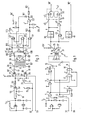
- FIG. 1 shows an isolating point circuit which enables the floating transmission of a digital data signal DA together with level information P F- via only one isolating point transformer 1.
- the circuit arrangement contains a square-wave signal generator 3 constructed in a manner known per se, the construction of which is not explained in more detail.
- the square wave at the output of the square-wave signal generator 3 is fed to a first conjunctive logic element 5, which can be released via its second input by the level information l y- E.
- the output signal of this first conjunctive logic element 5 controls a second conjunctive logic element 7 and a logic element 9 which is connected as a delaying inverter.
- the output c of this logic element 9 is connected to the input of a further logic element 11 which is also connected as a delaying inverter.
- the delay of the logic elements 9 and 11 is achieved by the signal propagation time of the logic elements themselves and by capacitors 13 and 15.
- the outputs c and d of the logic elements 9 and 11 are connected to the inputs of a third conjunctive logic element 17.
- both input signals Since the second input signal is inverted and delayed with respect to the first input signal, both input signals, due to the signal delay, assume zero potential only briefly at the same time for each pulse of the square wave of the square wave signal generator 3. In this way, 17 needle pulses are generated at the output f of this third conjunctive link, which have only a very short pulse duration.
- the second conjunctive logic element 7 is also supplied with the output signal of the logic element 9 and the data signal DA.
- this second conjunctive logic element 7 can be blocked or activated, so that needle pulses then occur at its output, which are derived in the manner described above from the positive edge of the square wave output at the output a of the square wave signal generator 3.
- the output e of the second conjunctive logic element 7 and the output f of the third conjunctive logic element 17 are connected to the inputs of a first disjunctive logic element 19, in which the output signals of the second and third conjunctive logic element 7, 17 are combined.
- the number of needle pulses appearing at the output g of the first disjunctive link 19 is only half as large compared to the case that the second conjunctive link 7 by the data signal DA is enabled, so that e needle pulses are also output at its output.
- the output g of the first disjunctive link 19 is connected via a capacitor 21 to one terminal 23 of the primary winding 25 of the isolating point transformer 1, the other terminal 27 of which is at ground potential.
- the separation point transformer 1 is designed with only a few turns, since this is sufficient for the transmission of needle pulses.
- While the secondary winding 29 is at ground potential at its one terminal 31, it is connected at its other terminal h to the control electrode 33 of a switching transistor 35, at whose collector terminal i the needle pulses to be used on the secondary side occur. While the emitter terminal 37 of the switching transistor 35 is at ground potential, its output terminal i with the supply voltage + 5V, with the input of a first monostable circuit 39, further with the input of a second monostable circuit 41 and finally with the free input of a ge as an inverter switched link 43 connected. While the first monostable circuit 39 has a switching time that lies between the single and double the minimum distance of the needle pulses, the switching time of the second monostable circuit 41 is longer than twice the minimum distance of the needle pulses.
- the output 1 of the first monostable circuit 39 is connected on the one hand to the set input 45 of a bistable circuit 47 and on the other hand to an input of a fourth conjunctive logic element 49, the second input of which is connected to the output k of the logic element 43 and the output signal of which is the reset input 51 of the bistable Circuit 47 controls, at the output of which the restored data signal DA 'appears.
- the bistable circuit 47 is formed by correspondingly connecting two OR gates 48 and 50 with inverting inputs.
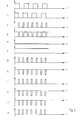
- the square wave signal shown in FIG. 2a is generated with the aid of the square wave signal generator 3. Contrary to the illustration in FIG. 2, the frequency of this square wave should be at least a factor 10 higher than the frequency of the data signal DA in order to keep the basic distortion of the data signal DA to be transmitted as small as possible.
- the signal designated PE in FIG. 2 is supplied to the first conjunctive logic element 5 in addition to the square wave as level information. If the level information PE has a positive potential, the first conjunctive link 5 is blocked. If, on the other hand, the voltage level 0 volts is present as level information at the input of the first conjunctive logic element 5, the high-frequency square wave (FIG. 2b) is fed to the further logic circuit 7, 9, 11, 17, 19.
- the high-frequency square wave is inverted by the logic element 9 and delayed with the support of the capacitor 13, so that the signal shown in FIG. 2c is produced at its output c. This is fed to the link 11, by means of which an inversion and delay is again carried out analogously to the link 9.
- the output signal of this logic element 11 is shown in FIG. 2d.
- the needle pulses shown in FIG. 2f are derived from the output signals of the two logic elements 9 and 11 (see FIGS. 2c and d) in the manner described above. Furthermore, in the event that the data signal DA assumes the voltage level 0 volt, the output signals (see FIGS. 2b and c) of the first conjunctive logic element 5 and the logic element 9 produce the needle pulses shown in FIG.
- the signal shown in FIG. 2g is generated at the output g of the first disjunctive logic element 19.
- the amplitude of the pulses therefore corresponds to the supply voltage of the logic elements. For example, it can be larger for a transmitting circuit than for a receiving circuit or vice versa. Since signals of small amplitude are usually sufficient on the line side, the logic links therefore only have to be supplied with a low supply voltage, which results in considerable power savings: low power consumption is also favored by the fact that the needle pulses have only a small voltage-time area.
- the signal shown in FIG. 2g is transmitted via the isolating point transformer 1, which effects the actual galvanic isolation, so that the signal shown in FIG. 2h appears at connection h.
- This is fed to the switching transistor 35.
- This acts as a pulse shaper, so that the signal shown in Fig. 2i arises.
- This is inverted by the logic element 43, so that the pulse train shown in FIG. 2k is produced at its output.
- the output signal of the switching transistor 35 shown in FIG. 2i is fed to the second monostable circuit 41 in addition to the first monostable circuit 39. Since the latter has a switching time which is longer than twice the minimum distance between the needle pulses applied to its input, its output signal PE '(see also FIG.
- bistable circuit 47 is set with the negative edge of the output signal of this first monostable circuit 39, while it is reset by the output signal (FIG. 2 m) of the fourth conjunctive logic element 49. This makes it possible for the data signal to be restored from the occurrence of the needle impulses with minimal or with twice the minimal distance. It appears as signal DA '(FIG. 2) at the output of bistable circuit 47.
- a second embodiment of a circuit arrangement for floating transmission of digital signals via separation points is shown, in which, in contrast to the first embodiment described above, in which the data signal was characterized by the spacing of the needle pulses, the state of the data signal by the polarity of the Needle impulses is marked.
- It contains a square-wave signal generator, generally designated 53, which is constructed in a known manner and is therefore not described in detail.
- the square wave output at the output of the square-wave signal generator 53 is fed directly to one input 55 of a first exclusive-OR gate 57 and the other input 59 thereof upstream of an RC gate 61 causing a delay, with the result that this first exclusive is output 63 -OR limb 57 needle impulses arise.
- the output 63 of this first exclusive-OR gate 57 is connected on the one hand to one input 65 of a second exclusive-OR gate 67 and on the other hand to the drain terminal 69 of a field effect transistor 71. If there is no defined level information PE at the control input 73 of the field effect transistor 71, the latter is controlled to be conductive since the control electrode 73 is connected to a positive potential via a resistor 75. When the field effect transistor 71 is switched on, the output 63 of the first exclusive OR element 57 is connected to ground potential and is thereby blocked.
- the field effect transistor 71 is switched off, with the result that the needle pulses at the output 63 of the first exclusive OR gate 57 reach the second exclusive OR gate 67.
- the needle pulses can be inverted as a function of the state of the data signal DA via the second input 77 of the second exclusive OR gate 67.
- the output 79 of the second exclusive OR gate 67 is connected via a decoupling capacitor 81 to the one terminal 83 of the primary action 85 of a separation point transformer 87.
- the other terminal 89 of the primary winding 85 of the isolating point transformer 87 is connected to the output 91 of a third exclusive OR element 93, one input 95 of which is at ground potential and the other input 97 of which is controlled by the data signal DA.
- This third exclusive-OR gate 93 only serves to compensate for the potential shift at the isolating point transformer 87 caused by the pulse inversion.
- the isolating point transformer 87 has two secondary windings 99 and 101. While one connection of the two secondary windings 99, 101 is at ground potential, the free connection of the first secondary winding 99 to the control electrode 103 of a first transistor 1-OS and the free connection of the second secondary winding 101 connected to the control electrode 107 of a second transistor 109.
- the two transistors 105 and 109 are driven in phase opposition by the secondary windings 99 and 101 due to their opposite winding sense.
- the collector connections 111 and 113 of the transistors 105 and 109 are each connected on the one hand via a resistor 115 or 117 to the positive supply voltage potential and on the other hand to the set input 119 or reset input 121 of a bistable circuit 123, at the output 125 of which the restored data signal DA ' appears.
- the bistable circuit 123 is formed by connecting two NAND gates 127 and 129 accordingly.
- the signals occurring at the collectors 111 and 113 of the transistors 105 and 109 are supplied to a third NAND gate 131 for superimposition.
- the output signal of this third NAND gate 132 is rectified by a rectifier diode 133 and sieved by a filter circuit 135, so that after inversion by a fourth NAND gate 137, the restored level information PE is obtained at its output 139.
- the output 139 of the fourth NAND gate 137 is connected to the output 125 of the bistable circuit 123 via a clamp diode 141 and a resistor 143.
- FIG. 4 For a better understanding of the functioning of the circuit arrangement described above, a pulse diagram is shown in FIG. 4, which reproduces the signals at certain points in the circuit arrangement shown in FIG. 3. This pulse image will now be explained in connection with FIG. 3.
- FIG. 4b shows the square-wave oscillation occurring at the output of the square-wave signal generator 53, which is fed directly to the input 55 of the first exclusive-OR gate 57.
- the square wave shown in FIG. 4b is delayed by the R-C gate 61, so that the square wave shown in FIG. 4a arises, which is fed to the input 59 of the first exclusive-OR gate 57.
- the needle pulses shown in FIG. 4c are derived by this first exclusive OR gate 57. If there is a 0-VoIt signal level at the data signal input, the needle pulses are not inverted, so that the pulse sequence shown in FIG. 4c also appears at the output of the second exclusive-OR gate 67.
- the second exclusive OR gate 67 inverts the pulse sequence shown in FIG. 4c, so that the pulse sequence shown in FIG. 4d is produced at its output 79. If, in the event that the data signal DA assumes the 0 volt signal level, the pulse sequence shown in FIG. 4c is not inverted, there is also no potential shift at the interface transformer 87, which would have to be compensated for by the third exclusive-OR gate 93 . The output 91 of this exclusive OR gate 92 is then at the 0 volt potential according to FIG. 4e.
- the pulse sequence is inverted in the case of a data signal DA with a positive signal level
- the potential shift associated therewith at the isolating point transformer 87 is compensated for by the output signal of the third exclusive-OR element 93 shown in FIG. 4f.
- a voltage U thus arises at the primary winding 85 of the isolating point transformer 87, which has the pulse image shown in FIG. 4g for a data signal DA with 0 volt level and the pulse image shown in FIG. 4h for a data signal with a positive signal level.
- the signal curve shown in FIG. 4i results for the voltage U, the first secondary winding 99 of the isolating point transformer 87, and that in FIG.
- the voltage U 1 on the first secondary winding 99 of the isolating point transformer has the voltage curve shown in FIG. 41 and the voltage U 2 on the second secondary winding 101 of the isolating point transformer 87 has the voltage curve shown in FIG. 4 m.
- the two transistors 105 and 109 are driven either in phase opposition by the signals according to FIG. 4i or FIG. 4k or by the signals according to FIG. 41 or FIG. 4m.
Landscapes
- Engineering & Computer Science (AREA)
- Power Engineering (AREA)
- Computer Networks & Wireless Communication (AREA)
- Signal Processing (AREA)
- Dc Digital Transmission (AREA)
- Arrangements For Transmission Of Measured Signals (AREA)
Applications Claiming Priority (2)
| Application Number | Priority Date | Filing Date | Title |
|---|---|---|---|
| DE3512280 | 1985-04-03 | ||
| DE19853512280 DE3512280A1 (de) | 1985-04-03 | 1985-04-03 | Schaltungsanordnung zur erdfreien uebertragung digitaler signale ueber trennstellen |
Publications (3)
| Publication Number | Publication Date |
|---|---|
| EP0198263A2 true EP0198263A2 (fr) | 1986-10-22 |
| EP0198263A3 EP0198263A3 (en) | 1988-03-30 |
| EP0198263B1 EP0198263B1 (fr) | 1992-01-29 |
Family
ID=6267261
Family Applications (1)
| Application Number | Title | Priority Date | Filing Date |
|---|---|---|---|
| EP19860103805 Expired - Lifetime EP0198263B1 (fr) | 1985-04-03 | 1986-03-20 | Montage pour la transmission de signaux numériques sans mise à la terre par l'intermédiaire de points de séparation |
Country Status (2)
| Country | Link |
|---|---|
| EP (1) | EP0198263B1 (fr) |
| DE (2) | DE3512280A1 (fr) |
Cited By (6)
| Publication number | Priority date | Publication date | Assignee | Title |
|---|---|---|---|---|
| EP0332054A3 (en) * | 1988-03-09 | 1990-08-01 | Nixdorf Computer Aktiengesellschaft | Method for transmitting a digital signal and status information |
| WO1991014327A1 (fr) * | 1990-03-07 | 1991-09-19 | Siemens Aktiengesellschaft | Circuits de transmission a potentiel separe d'impulsions de n'importe quelles longueur et frequence pour la commande de circuits a transistors |
| EP0977406A1 (fr) * | 1998-07-17 | 2000-02-02 | Endress + Hauser Wetzer GmbH + Co. KG | Circuit de transmission de signaux numériques avec séparation galvanique |
| US6853685B1 (en) | 1998-07-17 | 2005-02-08 | Stephan Konrad | Circuit arrangement for the electrically isolated transfer of digital signals |
| WO2006010417A1 (fr) * | 2004-07-23 | 2006-02-02 | Tridonicatco Gmbh & Co. Kg | Circuit d'interface destine a la transmission de signaux numeriques |
| US10419251B2 (en) | 2002-09-18 | 2019-09-17 | Infineon Technologies | Digital signal transfer using integrated transformers with electrical isolation |
Families Citing this family (1)
| Publication number | Priority date | Publication date | Assignee | Title |
|---|---|---|---|---|
| DE4205241C2 (de) * | 1992-02-21 | 1997-12-18 | Itt Ind Gmbh Deutsche | Potentialfreie Datenübertragungseinrichtung |
Family Cites Families (6)
| Publication number | Priority date | Publication date | Assignee | Title |
|---|---|---|---|---|
| JPS5034181B1 (fr) * | 1969-12-13 | 1975-11-06 | ||
| BE759604A (fr) * | 1969-12-15 | 1971-04-30 | Svenska Dataregister Ab | Dispositif de transmission d'informations |
| DE2050994B2 (de) * | 1970-10-16 | 1972-04-27 | Nixdorf Computer Ag, 4790 Paderborn | Verfahren und schaltungsanordnung zur erdfreien uebertragung von gleichstromsignalen |
| DE2411871C2 (de) * | 1974-03-12 | 1984-09-13 | Nixdorf Computer Ag, 4790 Paderborn | Schaltungsanordnung zur erdfreien Übertragung von Signalen über Trennstellen in Fernmeldeanlagen |
| DE2826897C2 (de) * | 1978-06-19 | 1979-12-20 | Nixdorf Computer Ag | Schaltungsanordnung zur erdfreien Übertragung von Signalen über Trennstellen in Fernmeldeanlagen |
| DE2945465A1 (de) * | 1979-11-10 | 1981-05-21 | Hartmann & Braun Ag, 6000 Frankfurt | Schaltungsanordnung zur galvanischen trennung von gleich- und wechselstromsignalen |
-
1985
- 1985-04-03 DE DE19853512280 patent/DE3512280A1/de not_active Ceased
-
1986
- 1986-03-20 EP EP19860103805 patent/EP0198263B1/fr not_active Expired - Lifetime
- 1986-03-20 DE DE8686103805T patent/DE3683668D1/de not_active Expired - Lifetime
Cited By (8)
| Publication number | Priority date | Publication date | Assignee | Title |
|---|---|---|---|---|
| EP0332054A3 (en) * | 1988-03-09 | 1990-08-01 | Nixdorf Computer Aktiengesellschaft | Method for transmitting a digital signal and status information |
| WO1991014327A1 (fr) * | 1990-03-07 | 1991-09-19 | Siemens Aktiengesellschaft | Circuits de transmission a potentiel separe d'impulsions de n'importe quelles longueur et frequence pour la commande de circuits a transistors |
| EP0977406A1 (fr) * | 1998-07-17 | 2000-02-02 | Endress + Hauser Wetzer GmbH + Co. KG | Circuit de transmission de signaux numériques avec séparation galvanique |
| US6853685B1 (en) | 1998-07-17 | 2005-02-08 | Stephan Konrad | Circuit arrangement for the electrically isolated transfer of digital signals |
| US10419251B2 (en) | 2002-09-18 | 2019-09-17 | Infineon Technologies | Digital signal transfer using integrated transformers with electrical isolation |
| WO2006010417A1 (fr) * | 2004-07-23 | 2006-02-02 | Tridonicatco Gmbh & Co. Kg | Circuit d'interface destine a la transmission de signaux numeriques |
| AU2005266656B2 (en) * | 2004-07-23 | 2011-06-23 | Tridonicatco Gmbh & Co. Kg | Interface circuit for transmission of digital signals |
| US8358088B2 (en) | 2004-07-23 | 2013-01-22 | Tridonic Atco Gmbh & Co. Kg | Interface circuit for transmission of digital signals |
Also Published As
| Publication number | Publication date |
|---|---|
| DE3683668D1 (de) | 1992-03-12 |
| EP0198263A3 (en) | 1988-03-30 |
| EP0198263B1 (fr) | 1992-01-29 |
| DE3512280A1 (de) | 1986-10-09 |
Similar Documents
| Publication | Publication Date | Title |
|---|---|---|
| DE19520940A1 (de) | Anordnung zur galvanisch getrennten Übertragung von Hilfsenergie (Gleichspannung) und Informationen zu einer elektronischen Einheit | |
| DE2459885C2 (de) | Schaltung zur Dekodierung eines dynamisch modulierten Signals | |
| EP0101607A1 (fr) | Décodeur biphasé | |
| EP0198263B1 (fr) | Montage pour la transmission de signaux numériques sans mise à la terre par l'intermédiaire de points de séparation | |
| EP0977406B1 (fr) | Circuit de transmission de signaux numériques avec séparation galvanique | |
| DE2807916C3 (de) | Wecksignalgenerator zur Verwendung in einer Teilnehmerverbindungsschaltung | |
| DE2837882A1 (de) | Taktformer fuer integrierte halbleiter-digitalschaltungen | |
| DE2108320A1 (de) | Einrichtung zur Frequenz- und Phasenregelung | |
| DE2903860C2 (de) | Einrichtung zur Gleichstromversorgung eines Verbrauchers und zur gleichzeitigen Informationsübertragung über ein Aderpaar | |
| DE2555260C3 (de) | Treiberschaltung zur Umsetzung der Übergänge eines nichtsymmetrischen Datencode in eine Folge abwechselnd positiver und negativer, je einen Übergang anzeigender Impulse | |
| EP0058754B1 (fr) | Dispositif pour l'injection de signaux numériques dans un système filaire | |
| DE2352381C3 (de) | Impulsgeber | |
| DE2427603A1 (de) | Schaltungsanordnung zum nachbilden der wellenform von telegrafieschrittimpulsen mit digitalen mitteln | |
| DE3436284C2 (fr) | ||
| DE2826897B1 (de) | Schaltungsanordnung zur erdfreien UEbertragung von Signalen ueber Trennstellen in Fernmeldeanlagen | |
| DE2736522C2 (de) | Schaltungsanordnung zum Obertragen von Daten | |
| DE2443869A1 (de) | Digitaldatenuebertragungsanlage | |
| DE2737528C2 (de) | Dynamisches Schutzsystem | |
| DE3436277C2 (fr) | ||
| DE2760101C1 (de) | Inverter fuer dynamische Sicherheitssysteme | |
| DE1690543C2 (de) | übertragungssystem für Normal- und Spezialbefehle in Rundsteueranlagen | |
| DE2012179C3 (de) | Schaltungsanordnung zum Umsetzen von Fernschreibzeichen | |
| DE2141714C3 (de) | Einrichtung zur Erkennung von Daten | |
| DE2203780C3 (de) | Gleichspannungsisolierter empfangsseitiger Teilnehmeranschluß | |
| DE2534351C2 (de) | Verfahren und Schaltungsanordnung zur Umwandlung digitaler Signale |
Legal Events
| Date | Code | Title | Description |
|---|---|---|---|
| PUAI | Public reference made under article 153(3) epc to a published international application that has entered the european phase |
Free format text: ORIGINAL CODE: 0009012 |
|
| AK | Designated contracting states |
Kind code of ref document: A2 Designated state(s): AT BE CH DE FR GB IT LI LU NL SE |
|
| RBV | Designated contracting states (corrected) |
Designated state(s): BE DE FR GB IT NL SE |
|
| PUAL | Search report despatched |
Free format text: ORIGINAL CODE: 0009013 |
|
| AK | Designated contracting states |
Kind code of ref document: A3 Designated state(s): BE DE FR GB IT NL SE |
|
| 17P | Request for examination filed |
Effective date: 19880909 |
|
| 17Q | First examination report despatched |
Effective date: 19900911 |
|
| RAP3 | Party data changed (applicant data changed or rights of an application transferred) |
Owner name: SIEMENS NIXDORF INFORMATIONSSYSTEME AKTIENGESELLSC |
|
| GRAA | (expected) grant |
Free format text: ORIGINAL CODE: 0009210 |
|
| AK | Designated contracting states |
Kind code of ref document: B1 Designated state(s): BE DE FR GB IT NL SE |
|
| PG25 | Lapsed in a contracting state [announced via postgrant information from national office to epo] |
Ref country code: BE Effective date: 19920129 |
|
| REF | Corresponds to: |
Ref document number: 3683668 Country of ref document: DE Date of ref document: 19920312 |
|
| ITF | It: translation for a ep patent filed | ||
| GBT | Gb: translation of ep patent filed (gb section 77(6)(a)/1977) | ||
| ET | Fr: translation filed | ||
| PLBE | No opposition filed within time limit |
Free format text: ORIGINAL CODE: 0009261 |
|
| STAA | Information on the status of an ep patent application or granted ep patent |
Free format text: STATUS: NO OPPOSITION FILED WITHIN TIME LIMIT |
|
| 26N | No opposition filed | ||
| EAL | Se: european patent in force in sweden |
Ref document number: 86103805.7 |
|
| PGFP | Annual fee paid to national office [announced via postgrant information from national office to epo] |
Ref country code: GB Payment date: 19950213 Year of fee payment: 10 |
|
| PGFP | Annual fee paid to national office [announced via postgrant information from national office to epo] |
Ref country code: FR Payment date: 19950323 Year of fee payment: 10 |
|
| PGFP | Annual fee paid to national office [announced via postgrant information from national office to epo] |
Ref country code: SE Payment date: 19950330 Year of fee payment: 10 |
|
| PGFP | Annual fee paid to national office [announced via postgrant information from national office to epo] |
Ref country code: NL Payment date: 19950331 Year of fee payment: 10 |
|
| PGFP | Annual fee paid to national office [announced via postgrant information from national office to epo] |
Ref country code: DE Payment date: 19950518 Year of fee payment: 10 |
|
| PG25 | Lapsed in a contracting state [announced via postgrant information from national office to epo] |
Ref country code: GB Effective date: 19960320 |
|
| PG25 | Lapsed in a contracting state [announced via postgrant information from national office to epo] |
Ref country code: SE Effective date: 19960321 |
|
| PG25 | Lapsed in a contracting state [announced via postgrant information from national office to epo] |
Ref country code: NL Effective date: 19961001 |
|
| GBPC | Gb: european patent ceased through non-payment of renewal fee |
Effective date: 19960320 |
|
| PG25 | Lapsed in a contracting state [announced via postgrant information from national office to epo] |
Ref country code: FR Effective date: 19961129 |
|
| NLV4 | Nl: lapsed or anulled due to non-payment of the annual fee |
Effective date: 19961001 |
|
| PG25 | Lapsed in a contracting state [announced via postgrant information from national office to epo] |
Ref country code: DE Effective date: 19961203 |
|
| EUG | Se: european patent has lapsed |
Ref document number: 86103805.7 |
|
| REG | Reference to a national code |
Ref country code: FR Ref legal event code: ST |
|
| PG25 | Lapsed in a contracting state [announced via postgrant information from national office to epo] |
Ref country code: IT Free format text: LAPSE BECAUSE OF NON-PAYMENT OF DUE FEES;WARNING: LAPSES OF ITALIAN PATENTS WITH EFFECTIVE DATE BEFORE 2007 MAY HAVE OCCURRED AT ANY TIME BEFORE 2007. THE CORRECT EFFECTIVE DATE MAY BE DIFFERENT FROM THE ONE RECORDED. Effective date: 20050320 |