EP0198574A2 - Appareil et procédé pour la cohérence de copies de données dans un système de traitement de données à multiples antémémoires - Google Patents
Appareil et procédé pour la cohérence de copies de données dans un système de traitement de données à multiples antémémoires Download PDFInfo
- Publication number
- EP0198574A2 EP0198574A2 EP86300660A EP86300660A EP0198574A2 EP 0198574 A2 EP0198574 A2 EP 0198574A2 EP 86300660 A EP86300660 A EP 86300660A EP 86300660 A EP86300660 A EP 86300660A EP 0198574 A2 EP0198574 A2 EP 0198574A2
- Authority
- EP
- European Patent Office
- Prior art keywords
- data signal
- signal group
- cache memory
- data
- data processing
- Prior art date
- Legal status (The legal status is an assumption and is not a legal conclusion. Google has not performed a legal analysis and makes no representation as to the accuracy of the status listed.)
- Withdrawn
Links
Images


Classifications
-
- G—PHYSICS
- G06—COMPUTING OR CALCULATING; COUNTING
- G06F—ELECTRIC DIGITAL DATA PROCESSING
- G06F12/00—Accessing, addressing or allocating within memory systems or architectures
- G06F12/02—Addressing or allocation; Relocation
- G06F12/08—Addressing or allocation; Relocation in hierarchically structured memory systems, e.g. virtual memory systems
- G06F12/0802—Addressing of a memory level in which the access to the desired data or data block requires associative addressing means, e.g. caches
- G06F12/0806—Multiuser, multiprocessor or multiprocessing cache systems
- G06F12/0815—Cache consistency protocols
Definitions
- This invention relates generally to data processing systems and, more particularly, to data processing systems having at least one cache memory unit.
- cache memory units can result in storage of a data signal group in a plurality of locations.
- Each copy of a data signal group stored throughout the data processing system must be equivalent. Otherwise procedures must be instituted to avoid inconsistent results that can arise from independent manipulation of the copies of a data signal group by the components of the data processing system.
- This procedure can suffer from several disadvantages.
- the most important disadvantage arises because many implementations of this procedure require duplicate cache directories be associated with each data processing system so that entries of each cache memory unit are known and data signal groups stored in every cache memory unit can be identified. While the duplicate directories can limit the required bus activity the duplicate cache directories must have a plurality of communication paths to update the related control signals when data signal groups are being altered. Thus, this technique of data signal group verification is complex and requires additional apparatus in its implementation.
- related procedures identify one data signal group, typically the main memory data signal group, as being the "correct" signal group.
- This procedure requires that when a data group is updated, it must be stored in the main memory and then extracted when a data processing unit requires the data signal group.
- the main memory access is typically longer than a cache memory access and an undesirable increase in system bus traffic can result from this procedure.
- the present invention therefore provides a data processing system including 4memory unit, a system bus, data processing units and cache memory units, in which each cache memory unit has a data processing unit associated therewith, characterised in that it includes:
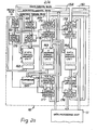
- FIG. 1 a block diagram of a data processing system having a plurality of data processing units is shown.
- the plurality of data processing units, data processing unit #1, 11, through data processing unit #n, 13, perform the manipulation of data signal groups under control of at least one system program.
- Cache memory unit #1, 16, is coupled to data processing unit #1, 11, and cache memory unit #n, 17, is coupled to data processing unit #n, 13.
- other data processing units now shown, can be coupled to associated cache memory units. All of the cache memory units are coupled to a system bus 15 and the system bus 15 is in turn coupled to main memory unit 19.
- the system bus is shown as including three sub-buses, a date signal bus 151, an address signal bus 152, and a control signal bus 153.
- the cache memory unit 16 is coupled to the system bus 15 and to the data processing unit 11 as follows.
- Control signal input register 168 receives signals from control signal bus 153, and applies signals to cache memory unit 161.
- Cache memory control unit 161 applies signals to control signal output register 175 and to state signal input register 171.
- State signal input register 171 applies signals to state signal memory unit 162.
- State signal memory unit 162 applies signals to cache memory control unit 161.
- Control signal output register 175 applies signals to control signal but 153.
- Address signal input selector 179 receives signals from address signal but.
- Address signal input register 167 applies signals to state signal memory unit 162, to y-address memory unit 163, to data signal memory unit 164, to address signal output selector 173, to comparator 165 and to address signal output register 177.
- Address signal output selector 173 and comparator 165 also receive signals from y-address signal memory unit 163.
- Address signal output register 177 also receives signals from address signal output selector 173 and applies signals to address signal bus 152.
- Data signal input selector 178 receives signals from data signal but 151, and data processing unit 11.
- Data signal unit register 166 receives signals from data signal input selector 178 and applies signals to data signal memory unit 164.
- Data signal output selector 174 receives signals from data signal memory unit 164 and from data processing unit 11 and applies signals to data signal output register 176.
- Data signal output register applies signals to data processing unit 11 and to data signal bus 151.
- the cache memory control unit 161 is coupled to data processing unit 11, to control signal output register 175, to control signal input register 168, to comparator 165, to address signal output selector 173, to address signal output register 177, to data signal output selector 174, to data signal output register 176; to state signal input register 171, to address signal input selector 179, to address signal input register 167, to data signal input selector 178, and to data signal input register 166.
- the structure of the address signal groups is defined.
- the address data signal group is divided into three subgroups; an x-address signal group 201 having q logic signal positions, a y-address signal group 202 having r logic signal positons, and a z-address signal group 203 having s logic signal positions.
- the x-address signal group defines a physical location of signal groups in the cache memory signal storage components.
- the y-address signal group is the portion of the address signal group stored in address signal group memory unit 163 at the x position when the data signal group corresponding to the address (x + y) is stored in the data signal group memory unit 164.
- the z group is an address signal group portion that is redundant when plurality of basic data signal groups (e.g. words) are transferred on the system bus simultaneously and identified by a single address signal group.
- the various signals and signal groups associated with and addressed by the x-address signal group is shown.
- state signal memory unit 162 a valid signal position 162a, an altered signal position 162b and a multiple signal position 162c are shown.
- y-address signal group memory unit 163 a y-address group is addressed.
- data signal group memory unit 164 a data signal group is addressed by a x-address signal group.
- State 1 and indeed the initial state of all cache memory units in a data processing system occurs when a location associated with the group of control signals does not have a data signal group in the associated data signal memory location, the data signal group therein is comprised of random data signals or is comprised of a data signal group that has been determined to be invalid.
- State 1 is interpreted by the data processing system associated with the cache memory unit as an empty memory location in the cache memory unit.
- State 2 is present when a valid data signal goupr is stored in the associated data signal group memory unit location.
- State 3 indicates that the data signal group having a predefined address has been accessed by the associated data processing unit, has been altered, and has been replaced in the memory location in the cache memory unit.
- State 4 provides an indication that the data signal, group memory location associated with the control signal register stores a data signal group that is also stored in at least one other cache memory unit and is identified by the identical address.
- State 5 is a state of the data signal group that is now allowed by the data processing system and defines the situation where the data signal groups in data signal group memory unit location associated with the control signal register cells is held in at least one additional cache memory unit, that the data signal group has been accessed by the associated data processing unit and has been altered, and that the altered data signal group has been returned to the same data signal group memory unit location.
- State 5 the activity that results from an attempt to assert the unpermitted State 5 of Figure 4 is summarized.
- the control signal memory unit locations assert either State 1 (not shown), State 4 or State 2 depending on the programmed response of the data processing unit to the attempt to assert State 5.
- State 4 indicates that the other versions of the data have been corrected and are still in the various cache memory units.
- State 2 indicates that the copies of the data in other cache memories has been rendered inaccessible or more accurately -invisible to the associated data processing unit by removal of the valid data bit from the associated control bit register cell.
- State 1 indicates that the altered data has been determined to be invalid and that memory location is considered to be empty.
- the address of the altered data is applied to the control bus, the altered data signal group is applied to the data signal bus.
- a "write" signal is asserted prior to communication of the address.
- the presence of the altered data control signal permits all other cache memory units to invalidate or to update the data signal group at the corresponding cache unit address.
- the main memory signal group is similarly updated at this time. It will be clear that for State 3, the architecture of the data processing system can support a delayed updating of the associated data signal group in the main memory. The problem present when other cache memory units store copies of non-updated data signal groups is not present here, because a cache memory unit requiring data at that address must communicate on the system bus.
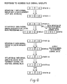
- FIG. 6 a summary is shown of the response of the cache memory unit to an address identified on the address signal group bus.
- the address on the address signal bus does not correspond to an address having an associated valid data signal group in the local cache memory unit. In this situation, the cache memory unit does not change state.
- the address on the address signal bus corresponds to an address of data requested by the local cache memory unit. In this case, the cache memory unit stores the associated data and changes the control signal bit to State 2. If a "multiple" signal is asserted on the control signal bus when the address signal group is applied to the address signal group, the control register cells signals are placed in State 4, indicating copies of the data exist in at least one additional cache memory unit.
- the local cache memory unit identifies an address on the address signal bus as being identified to a non-requested address in the cache memory unit.
- the control storage bits are changed to State 4 and a "multiple" signal asserted by the local cache memory unit on the control signal bus to insure that State 4 is applied to control register cells of the cache memory unit requesting and receiving the data signal group.
- the address, signal group on the address signal bus and an "altered" signal on the control signal bus causes the cache memory unit to place the control signal bits in State 4 or, as indicated in the discussion of Figure 5, to invalidate the data in the local cache memory unit in the local cache memory and place the associated control signal bit in State 1.
- the cache memory unit is a local memory for temporarily storing data signal groups that are more readily available to the associated data processing unit than are the data signal groups in the main memory.
- the cache memory unit can operate in either the "write back" or "write thru” mode of operation. This type of cache memory unit is distinguished by the mode of operation in which the result of every associated data processing unit operation is stored into the cache memory unit.
- the cache illustrated in Figure 2a and Figure 2b has another feature common to cache memory units.
- the address is divided into three parts.
- the first part (labelled x in Figure 2b) defines a physical location in the cache memory subunits.
- x defines a physical location in the cache memory subunits.
- the y-address signal group from the memory location can be compared with the y-address signal group of address signal input register 167. If these addresses are the same, the result is communicated to the cache memory control unit 161.
- the least significant signal bits are typically omitted when the data bus can transfer a plurality of basic data signal groups.
- the data signal groups are comprised of signal groups usually referred to as words and the data signals groups are always transferred in groups of two words, the final data bit can be omitted in the address (for purpsoes relevant to the instant invention).
- the final data bit can be omitted in the address (for purpsoes relevant to the instant invention).
- four words of data signals are identified by a single address, the final or some other defined location of the two address signals can be omitted.
- the operation of the cache memory unit is thus complicated by the use of first two subgroups of the address signal group. To determine if a data signal group is stored in the cache memory, it is first necessary to determine when the associated address signal group is stored in the cache memory unit. An address signal group is therefore entered in address signal input register 167.
- the x-portion of the address signal group is applied to the addressing mechanism of y-address signal memory unit 163.
- the contents of the physical location in memory unit 163 are applied to comparator 165 along with the y-address portion of the address signal group in address register 167. If the two y-address signal groups are identical, then the associated data signal group is stored in data signal group memory unit 164. However, the control bit signal register is simultaneously addressed at the x-address signal group position.
- a plurality of y-address signal group registers and associated data signal group registers can permit storage in the cache of a plurality of data signal groups with the same x-address signal groups.
- This technique requires increased storage apparatus as well as a more complex comparison procedure.
- a "hashing" algorithm can be utilized when a plurality or multiplicity of physical memory units is not practical.
- a “hashing" procedure provides a method of redefining address signal groups so that the normally clustered addresses are distributed throughout the memory address space.
- Still another technique to prevent address clustering is to use some internal portion of an address signal group as the x-address signal group. The present invention will function with any of these and other addressing techniques.
- the cache memory unit has the capability for receiving address signal groups from the address signal bus and for applying signals to the address signal bus.
- the cache memory unit can retrieve data signal groups from the data signal bus and can apply data signal groups to the data signal bus.
- control signals can be received from and applied to the control signal bus by the cache memory unit.
- the cache memory unit can supply requested data to the associated data processing unit, and can store data signal groups from the data processing unit.
- the function of the apparatus added to the data processing system to implement the states described by the present invention is to ensure that each data processing unit has available for manipulation only the most recent version of a data signal group.
- the assumption is made by the architecture that the most recent version of the data signal group is the "correct” version. Other assumptions concerning the "correct” version can be supported by the apparatus of the instant invention.
- the multiple locations in which the data signal groups can be stored, i.e. in the cache memory units associated with the data processing units and in the main memory is of concern in cache memory systems wherein data signal groups from the data processing unit are written back into the cache memory unit.
- the problem relates to the situation where an updated version of a data signal group can exist in one of a plurality of cache memory units while another cache memory unit can contain a "prior" version of the data signal group.
- the data processing unit attempting to store an altered data signal in the associated cache memory unit will temporarily store the altered data signal group in the data processing unit until access to the system but is obtained.
- the "altered” or "write” signal applied to the control signal bus by the local cache memory unit, informs all other cache memory units and the main memory that the data at that address placed on the address signal bus is not the correct "version” of the data. If the data signal group resides only in the main memory in addition to the local cache memory unit, then there is no urgency to correct this copy of data signal group. This lack of urgency is a result that any data processing unit requesting a data signal group must use the system bus.
- the address signal group asserted on the system bus for aquisition of the data signal group will be interrogated by every cache memory unit and the correct "version" of.the data signal group can be applied to the system bus. Thus the requesting cache memory unit will receive a "correct" version of the data.
- the local cache memory unit When more than one cache memory unit has a copy of the data signal group and one of the duplicated data signal groups is to be updated, it is necessary to correct all copies of the data signal group before the storage of the altered signal group in the cache memory unit.
- the "multiple" control signal bit is asserted by a local cache memory unit when a data signal group stored therein is requested by another data processing unit.
- the presence of the multiple signal in a local cache memory unit causes the local cache unit to signal via the "write" signal on the control bus that the associated data signal group(s) must be updated in each of the other cache memory units containing a copy of the data signal group.
- the updating is performed as soon as the data processing unit cache memory unit can gain access to the bus and prior to storage of the altered data signal group in the associated cache memory unit. Thus all copies are updated as soon as possible with the restrictions of the architecture of the data processing system.
Landscapes
- Engineering & Computer Science (AREA)
- Theoretical Computer Science (AREA)
- Physics & Mathematics (AREA)
- General Engineering & Computer Science (AREA)
- General Physics & Mathematics (AREA)
- Memory System Of A Hierarchy Structure (AREA)
- Information Retrieval, Db Structures And Fs Structures Therefor (AREA)
Applications Claiming Priority (2)
| Application Number | Priority Date | Filing Date | Title |
|---|---|---|---|
| US69836485A | 1985-02-05 | 1985-02-05 | |
| US698364 | 1985-02-05 |
Publications (2)
| Publication Number | Publication Date |
|---|---|
| EP0198574A2 true EP0198574A2 (fr) | 1986-10-22 |
| EP0198574A3 EP0198574A3 (fr) | 1989-11-29 |
Family
ID=24804925
Family Applications (1)
| Application Number | Title | Priority Date | Filing Date |
|---|---|---|---|
| EP86300660A Withdrawn EP0198574A3 (fr) | 1985-02-05 | 1986-01-31 | Appareil et procédé pour la cohérence de copies de données dans un système de traitement de données à multiples antémémoires |
Country Status (4)
| Country | Link |
|---|---|
| EP (1) | EP0198574A3 (fr) |
| JP (1) | JPS61246851A (fr) |
| AU (1) | AU5297186A (fr) |
| IE (1) | IE860319L (fr) |
Cited By (1)
| Publication number | Priority date | Publication date | Assignee | Title |
|---|---|---|---|---|
| EP0470574A3 (en) * | 1990-08-06 | 1992-07-08 | Fujitsu Limited | Multiprocessor system including cache memories and method of controlling cache memories to maintain coherence of data therebetween |
Family Cites Families (1)
| Publication number | Priority date | Publication date | Assignee | Title |
|---|---|---|---|---|
| US4695951A (en) * | 1983-07-07 | 1987-09-22 | Honeywell Bull Inc. | Computer hierarchy control |
-
1986
- 1986-01-31 EP EP86300660A patent/EP0198574A3/fr not_active Withdrawn
- 1986-02-04 IE IE860319A patent/IE860319L/xx unknown
- 1986-02-04 AU AU52971/86A patent/AU5297186A/en not_active Abandoned
- 1986-02-05 JP JP61022196A patent/JPS61246851A/ja active Pending
Cited By (1)
| Publication number | Priority date | Publication date | Assignee | Title |
|---|---|---|---|---|
| EP0470574A3 (en) * | 1990-08-06 | 1992-07-08 | Fujitsu Limited | Multiprocessor system including cache memories and method of controlling cache memories to maintain coherence of data therebetween |
Also Published As
| Publication number | Publication date |
|---|---|
| IE860319L (en) | 1986-08-05 |
| AU5297186A (en) | 1986-08-14 |
| EP0198574A3 (fr) | 1989-11-29 |
| JPS61246851A (ja) | 1986-11-04 |
Similar Documents
| Publication | Publication Date | Title |
|---|---|---|
| US4847804A (en) | Apparatus and method for data copy consistency in a multi-cache data processing unit | |
| US4471429A (en) | Apparatus for cache clearing | |
| US6047357A (en) | High speed method for maintaining cache coherency in a multi-level, set associative cache hierarchy | |
| US4977498A (en) | Data processing system having a data memory interlock coherency scheme | |
| US5237694A (en) | Processing system and method including lock buffer for controlling exclusive critical problem accesses by each processor | |
| EP0072179B1 (fr) | Effacement d'adresses invalides dans une mémoire cache | |
| US5406504A (en) | Multiprocessor cache examiner and coherency checker | |
| US5226144A (en) | Cache controller for maintaining cache coherency in a multiprocessor system including multiple data coherency procedures | |
| US5095424A (en) | Computer system architecture implementing split instruction and operand cache line-pair-state management | |
| US5627993A (en) | Methods and systems for merging data during cache checking and write-back cycles for memory reads and writes | |
| US5740400A (en) | Reducing cache snooping overhead in a multilevel cache system with multiple bus masters and a shared level two cache by using an inclusion field | |
| US4410944A (en) | Apparatus and method for maintaining cache memory integrity in a shared memory environment | |
| EP0347040B1 (fr) | Système de mémoire de données | |
| US6625698B2 (en) | Method and apparatus for controlling memory storage locks based on cache line ownership | |
| US6662276B2 (en) | Storing directory information for non uniform memory architecture systems using processor cache | |
| EP0343567A2 (fr) | Système multiprocesseur et dispositif d'antémémoire pour y être utilisé | |
| US6560681B1 (en) | Split sparse directory for a distributed shared memory multiprocessor system | |
| US6065099A (en) | System and method for updating the data stored in a cache memory attached to an input/output system | |
| US5802567A (en) | Mechanism for managing offset and aliasing conditions within a content-addressable memory-based cache memory | |
| EP0474450A2 (fr) | Système de processeur avec des moyens de transfert de mémoire | |
| EP0533427B1 (fr) | Système de commande de mémoire d'ordinateur | |
| GB2065941A (en) | Cache store system | |
| JPH04336641A (ja) | 処理システムにおける使用のためのデータキャッシュおよび方法 | |
| EP0153109B1 (fr) | Système à cohérences d'antémémoires | |
| US6021466A (en) | Transferring data between caches in a multiple processor environment |
Legal Events
| Date | Code | Title | Description |
|---|---|---|---|
| PUAI | Public reference made under article 153(3) epc to a published international application that has entered the european phase |
Free format text: ORIGINAL CODE: 0009012 |
|
| AK | Designated contracting states |
Kind code of ref document: A2 Designated state(s): AT BE CH DE FR GB IT LI LU NL SE |
|
| PUAL | Search report despatched |
Free format text: ORIGINAL CODE: 0009013 |
|
| AK | Designated contracting states |
Kind code of ref document: A3 Designated state(s): AT BE CH DE FR GB IT LI LU NL SE |
|
| STAA | Information on the status of an ep patent application or granted ep patent |
Free format text: STATUS: THE APPLICATION IS DEEMED TO BE WITHDRAWN |
|
| 18D | Application deemed to be withdrawn |
Effective date: 19900530 |
|
| RIN1 | Information on inventor provided before grant (corrected) |
Inventor name: WARREN, RICHARD ALAN Inventor name: SHAFFER, STEPHEN JAY |